A Synthetic Ripple Buck Converter with Dynamic Hysteretic Band Modulation
C.T. Tsai H.P. Chou
Graduate Student Department of Engineering and
System Science National Tsing Hua University Hsinchu, Taiwan
imdago0925@gmail.com
Abstract -- This paper presents an integrated DC-DC buck converter using the synthetic ripple hysteresis control scheme with a fast transient path to define the boundary of hysteresis band. The hysteresis band and switching frequency depend on load current changes; therefore, it accelerates regulation and reduces overshoot. Full chip simulation results indicated output voltage recovery time is shortened within 10µs under load current condition between 100mA to 500mA. The present work requires no external compensation capacitors and can be implemented with integrated technology for on-chip applications.
Index Terms—Fast transient, Hysteresis, Hysteretic Band Modulation
I. INTRODUCTION
Portable electronics products such as cellular phones, laptops and diverse multimedia equipments use battery as the main power source. To extend battery life, portable devices stay in sleep mode with a very low static current but require a fast wake-up to reach the normal mode with a much higher operational current.
Figure 1 illustrates the basic structure of a pulse width modulation (PWM) DC-DC converter [1]. Output power
Fig. 1. Schematics of conventional PWM buck converter.
MOSFETs is controlled by the PWM signal with its pulse width depending on the output error and a fixed frequency ramp signal. The system compensation block is to increase system stability margin for closed loop operation. The large capacitance used for frequency compensation increases
Professor
Department of Engineering and System Science
National Tsing Hua University Hsinchu, Taiwan
hpc@mx.nthu.edu.tw
response time; it is often too large to be integrated for on-chip applications. Various fast transient control techniques were proposed. [2]-[6]. The enhanced V2 control scheme [2] senses current ripple and stacks with feed-forward output voltage, hence the stacked signal reflects immediate variation of output voltage. The stacked signal is then compared with output error signal to generate a PWM signal. The V2 control scheme has a fast response by modulating the PWM signal in advance with the output voltage. The scheme is, however, has a large overshoot caused by rapid variations of the duty cycle of the PWM signal in fast transient operations. Besides, the V2 control scheme still needs external frequency compensation capacitors for stability considerations.
Another popular control technique named hysteresis control is well known by its fast response and simple structure [3-4]. The ripple signal sensed from inductor current or output voltage is confined within a hysteretic band and used to control the power MOSFETs with simple logic gates.
Hysteresis control is self-stabilized so additional frequency compensation capacitor is not needed; therefore, leads to a very fast response. However, the scheme requires the ripple signal with a magnitude to overcome switching noise; on the other hand, the magnitude of the ripple is limited by the equivalent series resistance (ESR) of output capacitors. To solve the noise problem, a synthetic-ripple modulator (SRM) technique [5] was introduced to generate a noise-free ripple signal and insensitive to the value of inductors.
Implementation of the SRM technique, however, requires a large chip area and is not suitable for on-chip regulators.
The present buck converter is based on the hysteresis control scheme with an integrated SRM to reduce chip area for on-chip regulators. According to the idea of the V2 control scheme, the ripple signal is stacked with error signal to immediately reflect output variation and accelerate transient response. Compared with previous designs, we proposed a hysteretic band modulator to mitigate the overshoot problem and applied a large closed loop gain to reduce regulation errors.
The proposed circuit configuration and operation principle are described in detail in section II. Circuit implementation for the proposed scheme is described in section III. Full-chip simulation results are presented in section IV to verify proposed method.
II. OPERATION PRINCIPLE
The structure of the buck converter with proposed fast transient hysteresis control is shown in Fig. 2. The Vref and Vfb are fed to the error amplifier which generates an error voltage VLB to reflect the output voltage Vout variation immediately. The ripple signal Vripple, is generated by the synthetic ripple modulator with a hysteretic band confined by VLB and VHB. The lower limit of the hysteretic band VLB is stacked with a variable positive voltage Vhys which is generated from hysteretic band modulator to define the higher band limit VHB. Vripple, VLB and VHB are then sent into a hysteresis comparator. The hysteresis comparator output signal is sent to the fixed dead-time buffer to generate a pair of non-overlapping gated signals, the signal is strengthened by digital driver block to increase the driving ability for power MOSFETs. A soft-start circuit is added to prevent the large inrush current damage during the start-up transient response.
Fig. 2. Schematics of buck converter with proposed hysteresis control scheme
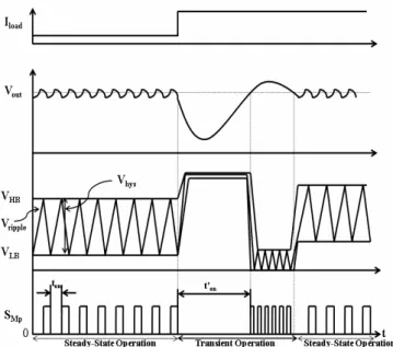
Operational waveforms of the proposed fast transient controller are illustrated in Fig. 3. As shown in Fig. 3, the ripple is stacked on VLB and regulated within the hysteretic band which is named Vhys. In steady state operation, switching frequency is a constant due to the fixed hysteretic band. When the load current varies, rapid variation of Vout enables the fast transient mechanism for rapid adjustment. There are two control steps; in one step, the power MOSFETs is to adjust the output current in one switching period; in another step, the hysteretic band Vhys is modulated to adjust the switching frequency. The two steps exchanges in step-up and step-down load transient, respectively. During transient response, VLB changes rapidly and the switching period can be modulated immediately, hence fast transient response can be achieved.
Fig. 3. Transient operation waveforms of proposed control.
III. CIRCUIT IMPLEMENTATION
A. Integrated Synthetic Ripple Modulator
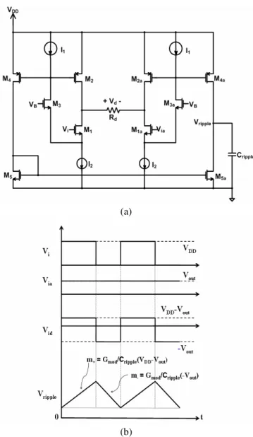
To reduce chip area for on-chip applications, an integrated synthetic ripple modulator is developed to generate the ripple signal for hysteresis control. Detail schematics of the proposed modulator are illustrated in Fig. 4(a). The synthetic ripple modulator acts like a trans-conductance amplifier. M1 and M1a are level shifters and the difference voltage Vd across resistor Rd is to bias M1 and M1a differently. M2-M3 and M2a- M3a pairs form the negative feedback paths to improve nonlinearity. M2-M4 and M2a-M4a pairs are current mirrors which program the output current. The total trans- conductance, Gmod, can be derived as (1):
2 .
2 1
mod
= k
k G R
d
(1)
where k1 and k2 are the weighted factors depending on the aspect ratio of M2-4 and M2a-4a pairs. Relationship between the input and output voltage waveform in steady-state operation is shown in Fig.4 (b).
(a)
(b)
Fig. 4. (a) Schematics of the proposed integrated synthetic ripple modulator and its (b) input and output waveforms in steady-state operation.
According to Fig. 2, each input of the modulator is connected to two terminals of the inductor L, respectively. The differential input signal Vid varies from positive to negative value in one switching period and generates the bi-directional output current Id+ and Id-. The output current charges- discharges the output capacitor Cripple in one switching period and the associated output voltage Vripple can be derived as (2):
ripple off d ripple
on T d
ripple d ripple
C T I C
T dt I C
V =∫0s I = + + − (2)
where Ton and Toff are the on and off time of the power MOS in one period; Ts is the switching period. These parameters are defined in (3) – (5):
+
=
d ripple hys
on I
C
T V (3)
.
−
=
d ripple hys
off I
C
T V (4)
s d
ripple hys d
ripple hys off on
s I f
C V I
C T V
T
T 1
= +
= +
=
− +
(5)
Through the above relations, as shown in Fig. 4 (b), a noise- free triangular signal is generated for hysteresis control.
B. Hysteretic Band Modulator
To determine the switching frequency and timing of modulation, a hysteretic band modulator is developed as shown in Fig. 5. In the first stage, M1 is biased according to the desired discharge current of Chys; M2 and M3 are current mirrors to replicate the desired discharge current of Chys. M4 and M6 are enabled by Vft from output detector circuit shown in Fig. 5; M4 and M6 do not turn on at the same time, hence Vhys can be held at a fixed level. M5 acts like a switch for the discharge path which is opened while Vhys falls to a specified lower limit, VL. Obviously, Vhys is also restricted under higher limit, VH.
Fig. 5. Schematics of the proposed hysteretic band modulator for fast transient control
Fig. 6. Timing control waveforms of proposed hysteretic band modulator
The timing control and operation waveform of the hysteretic band modulator are illustrated in Fig. 6. The second stage of the proposed scheme is a voltage adder [7] which defines the top boundary of hysteretic band, VHB. Vhys is fed into the second stage as one of the inputs. An operation amplifier and M7 form a negative feedback loop to ensure that the inverting input is the same voltage level as Vhys. The current through R1 is copied by M8 and M9; hence the voltage drop across R2 is equal to Vhys. The drain voltage of M9 named VHB can be consequently derived as (6):
hys.
LB
HB V V
V = + (6) where VHB is the top boundary of hysteretic band.
In summary, the function of the hysteretic band modulator is to determine the timing of hysteretic band modulation and the upper limit of the hysteretic band VHB, so that a stable yet fast response can be realized.
IV. SIMULATION RESULT
The proposed buck converter is designed and simulated using a 0.35 µm CMOS process. The inductor and capacitor of the power stage are 10 µH and 4.7 µF, respectively, where ESR of the capacitor is 200 mΩ. The nominal switching frequency is 2MHz and the desired VOUT is 2V with the input voltage range between 3V and 4.2V. The maximum load current is 500 mA, and the output voltage ripple is no more than 5mV.
Figure 7(a) shows a step-up load transient, where load current Iload varies from 100 mA to 500 mA. To show the details of proposed fast transient control, the key operation waveforms are also illustrated in Fig. 7 (a). The recovery time and overshoot is 9 µs and 90 mV respectively. As described in section II, the two steps of control are realized. Figure 7 (b) shows the simulation of step-down condition, where the load current varies from 500 mA to 100 mA. The recovery time is 8 µs and overshoot is 115 mV.
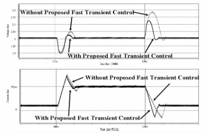
Comparisons were made to verify the transient performance with and without using the proposed fast transient technique in hysteresis control scheme. As shown
in Fig. 8, the controller with the proposed control scheme shortens the recovery time and the overshoot both by about 20% in the step-up load transient response; in the step-down load transient response, the recovery time and the overshoot are reduced by about 30%. The comparisons clearly indicated that the proposed control method can improve fast transient response; the detail specifications of the proposed design are listed in Table I. Full chip layout diagram is shown in Fig. 9.
(a)
(b)
Fig. 7. The output voltageand Vripple waveforms of the proposed control scheme (a) when Iload changes from 100 mA to 500 mA; (b) when Iload
changes from 500 mA to 100 mA.
Fig. 8. The output voltageand inductor current of synthetic ripple hysteresis converter with / without the proposed fast transient control while
Iload changes bêtween 100 mA to 500 mA.
TABLEI
SPECIFICATIONS OF PROPOSED FAST RESPONSE HYSTERESIS BUCK CONVERTER
Technology TSMC 0.35um 2P4M CMOS process
Inductor 10μH
Output Capacitor 4.7µF
ESR of Output Capacitor 200mΩ
Input Voltage Supply Range Load Current Range
Output Voltage Output Voltage Ripple
Recovery Time of Load Transient Maximum Output Voltage
Overshoot
3.0-4.2V
100mA-500mA 2V
<20mV 9µs (100mA to 500mA) 8µs (500mA to 100mA) 90mV (100mA to 500mA) 115mV (500mA to 100mA)
Conversion Efficiency Max. 93.89%
1.914mm 2.096mm
Fig. 9. Full chip layout diagram of this work.
V. CONCLUSION
A synthetic ripple hysteresis controller has been developed.
The hysteretic band and switching frequency depend on load current changes; therefore, it accelerates regulation and reduces overshoot. The synthetic ripple modulator generates a stable and noise-free signal and does not require large external capacitors for frequency compensation and therefore is appropriate for small area applications such as portable devices. Simulation results indicated the converter can achieve fast regulation within 10µs for a load current range between 100 mA and 500 mA.
ACKNOWLEDGMENT
The work is part of the research project under the support of National Science Council, Taiwan. We would like to thank the National Chip Implementation Center for their support in microelectronic circuit fabrication and development.
Assistance from Prof. K. H. Chen is grateful.
REFERENCES
[1] W. Erickson and D. Maksimovic, Fundamentals of Power Electronics.
Norwell, MA: Kluwer, 2001.
[2] W. Huang, “A new control for multi-phase buck converter with fast transient response,” in Proc. IEEE APEC’01 Conf., pp. 273-279.
[3] J. Abu-Qahouq, H. Mao, and I. Baterseh, “Multiphase voltage-mode hysteretic controlled dc-dc converter with novel current sharing,”
IEEE Trans. Power Electron., vol. 19, no.6, pp.1397-1407, Nov. 2004.
[4] Chunping Song; Nilles, J.L., “ High-accuracy hysteretic current-mode regulator for powering microprocessors,” in Proc. IEEE APEC’06 Conf., pp. 19-23.
[5] K.D.T. Ngo, S. K. Mishra, and M. Walters, “Synthetic ripple modulator for synchronous buck converter,” IEEE PE Letter, vol. 3, pp.
148-151, Dec. 2005.
[6] Yu-Huei Lee; Shih-Jung Wang; Chun-Yu Hsieh; Ke-Horng Chen,”
Current mode DC-DC buck converters with optimal fast-transient control, ” in Proc. IEEE ISCAS 2008 Conf., pp. 13-21.
[7] M. Siu, P. K. T. Mok, K. N. Leung, Y. H. Lam, and W. H. Ki, “A voltage-mode PWM buck regulator with end-point prediction” IEEE Trans. Circuits and Systems II, vol. 53, no. 4, pp. 294-298, Apr. 2006.
[8] C. F. Lee and P. K. T. Mok, “A monolithic current-mode CMOS DC- DC converter with on-chip current-sensing technique,” IEEE J. Solid- State Circuits, vol. 39, no. 1, pp. 3-14, Jan. 2004.
![Figure 1 illustrates the basic structure of a pulse width modulation (PWM) DC-DC converter [1]](https://thumb-ap.123doks.com/thumbv2/9libinfo/9127756.411912/1.892.75.436.758.972/figure-illustrates-basic-structure-pulse-width-modulation-converter.webp)