Enhanced efficiency of GaN-based light-emitting diodes with periodic textured Ga-doped ZnO transparent contact layer
Jinn-Kong Sheua兲and Y. S. Lu
Institute of Electro-Optical Science and Engineering, National Cheng Kung University, Tainan 70101, Taiwan
Min-Lum Lee
Department of Electro-Optical Engineering, Southern Taiwan University, Tainan 71005, Taiwan W. C. Lai
Institute of Electro-Optical Science and Engineering, National Cheng Kung University, Tainan 70101, Taiwan
C. H. Kuo
Department of Optics and Photonics, National Central University, Taoyuan 320, Taiwan Chun-Ju Tun
National Synchrotron Radiation Research Center, Hsinchu 30076, Taiwan
共Received 22 May 2007; accepted 7 June 2007; published online 28 June 2007兲
GaN-based light-emitting diodes 共LEDs兲 with indium tin oxide 共ITO兲/Ga-doped ZnO 共GZO兲 composite oxide films serving as a transparent contact layer共TCL兲 were demonstrated. In this study, the wall-plug efficiency of LEDs 共LED-III兲 with textured ITO/GZO composite TCL can be markedly improved by 200% and 45% of magnitude as compared to conventional LEDs with Ni/ Au TCL共LED-II兲 and planar ITO/GZO TCL共LED-I兲, respectively. Compared to LED-II, this enhancement is due to the enhanced light extraction efficiency of ITO/GZO composite TCL with high transparency. Compared to LED-I, ZnO-based TCL with a higher refractive index 共n⬃2.0兲 allows further enhancement of light extraction through the creation of a textured structure on transparent conductive oxide TCL deposited on the top surface of LEDs. In addition, the ITO/GZO composite TCL with a thickness of 550 nm is far larger than that of Ni/ Au TCL with a thickness of approximately 15 nm. Therefore, in addition to the effect of high transparency, the thicker ITO/GZO TCL with low lateral resistance would also act as a current-spreading layer leading to an enhancement of light extraction. © 2007 American Institute of Physics.关DOI:10.1063/1.2753110兴
The development of high-efficiency InGaN light- emitting diodes共LEDs兲 is considered one of the most impor- tant topics in the area of solid-state lighting.1 However, the efficiency of LEDs is limited by several factors including the high resistivity of p-GaN; hence, the severe current crowding occurs under the p electrode. For this reason, a thin Ni/ Au layer with transparency below 70% in the visible region has been extensively investigated to serve as the transparent con- tact layer 共TCL兲.2 Transparent conductive oxides 共TCO兲, such as indium tin oxide 共ITO兲, have high transparency in the visible region, allowing it to serve as the TCL in LEDs.3–6 ZnO-based TCO is a well-known wide band gap material and an alternative substance for a TCL in LEDs.7,8It has similar electrical and optical properties to ITO, but it is a nontoxic material, which has high temperature stability and costs less to manufacture.8 Recent research demonstrated that using ZnO doped with gallium resulted in films both with low resistivity and high transmittance in the visible region.9
The light extraction efficiency共LEE兲 of LED devices is mainly governed by the probability that a photon emitted from the active layer will escape from the high-refractive- index semiconductor material into the lower-refractive-index surrounding material, i.e., air or resin.1To enhance the prob-
ability of escape for photons generated in the active layer of the LED, the angular randomization of photons can be achieved through surface scattering from the roughened top surface of the LED.4 In addition to high transparency, ZnO- based TCL with a higher refractive index 共n⬃1.9–2.1兲 al- lows further enhancement of light extraction through the cre- ation of a textured structure on the ZnO-based TCL deposited on the top surface of LEDs. In this study, GaN- based LEDs with a periodic textured structure performed on the Ga-doped ZnO共GZO兲 TCL instead of the p-GaN layer were designed to further increase the LEE. Typically, ZnO- based TCO prepared by magnetron sputtering can achieve a refractive index of around 2 in the visible region. Therefore, GZO films with a textured surface were used as the TCL on InGaN blue LEDs to achieve a marked enhancement in light output power compared to LEDs with Ni/ Au or planar GZO TCL.
The InGaN / GaN multiple-quantum-well LED wafers used in this study were grown on c-face sapphire 共0001兲 substrates by metal organic vapor phase epitaxy. The detailed layer structure and growth procedure have been described in previous publication.4For LEDs with planar ITO/GZO com- posite TCL共LED-I兲, a 30-nm-thick ITO film was first depos- ited onto the p-GaN layer using an electron beam evaporator, and then the GZO film with a 3% Ga content was deposited on the aforementioned samples using a magnetron sputtering method. The total thickness of the ITO/GZO composite TCL
a兲Author to whom correspondence should be addressed;
APPLIED PHYSICS LETTERS 90, 263511共2007兲
0003-6951/2007/90共26兲/263511/3/$23.00 90, 263511-1 © 2007 American Institute of Physics
Downloaded 22 Oct 2009 to 140.116.208.44. Redistribution subject to AIP license or copyright; see http://apl.aip.org/apl/copyright.jsp
was 550 nm. ZnO and Ga2O3targets were used as the sput- tering sources during the cosputtering deposition of the GZO films.9The samples were then annealed at 800 ° C for 1 min in ambient N2 in a rapid thermal annealing system. In this study, LEDs with Ni 共5 nm兲/Au 共10 nm兲 TCL were also prepared for the purpose of comparison and were labeled as LED-II. For the fabrication of LED-IIs, after the deposition of Ni/ Au, the samples were annealed at 550 ° C in ambient air for 5 min. Periodic texture was performed on the GZO TCL by photolithography and a wet etching process using a dilute HCl solution共HCl:H2O = 1 : 4兲 to create a 5-m-wide GZO strip, while the spacing between two GZO strips was kept at 10m. The etching depth of the GZO layer was around 370 nm. Figures1共a兲and1共b兲illustrate the schematic device structure with a cross-section view and a top-view graph of the InGaN / GaN LEDs with periodic texture on the GZO TCL, respectively. In this study, LEDs with textured GZO TCL were labeled as LED-III. In this study, all fabri- cated LEDs had a dominant emission wavelength of 460 nm.
The current-voltage 共I-V兲 characteristics of experimental LEDs were measured using the HP-4156C semiconductor parameter analyzer, and the output power of the LEDs was measured with a calibrated integrating sphere.
The forward voltages 共Vf兲 measured at 20 mA were equal to 3.65, 3.3, and 3.75 V for the LED-I, LED-II, and LED-III, respectively, as shown in Fig.2. It should be noted that LEDs with GZO directly deposited onto the p-GaN layer exhibit poor electrical properties with typical Vf values as high as 5 V. Similar results were also obtained for the GaN- based LEDs with Al-doped ZnO TCL.8This can be attributed to the fact that the resistivity 共electron concentration兲 of GZO is still not low共high兲 enough to form a low-resistivity Ohmic contact and may even result in a Schottky contact. In other words, the GZO/ p-GaN contact with a high Schottky barrier hinders the carrier from transporting through the in- terface. To further reduce the Vf of LEDs with GZO TCL, a thin ITO layer, which has resistivity as low as ⬃1
⫻10−4⍀ cm, was inserted between the GZO and p-type
GaN. This scheme differs from previous reports using a thin Ni or NiOxlayer, which has a lower transparency compared to ITO thin layer, to improve the electrical performance of GaN LEDs with TCO layers as the TCL.5,7,8As depicted in Fig. 2, LED-I and LED-III exhibit a Vf of around 3.7 V when the low-resistivity ITO layer was inserted between the GZO and p-type GaN layer. This improvement could be at- tributed to the fact that an ITO with low resistivity can lead to an Ohmic contact rather than a Schottky contact, which was observed in the GZO/ p-type GaN contact.
With an injection current of 20 mA, the light output powers are 4.5 and 2.08 mW for LED-I and LED-II, respec- tively, as shown in Fig. 2. Although the output power of LED-I was much higher than that of LED-II, we should note that the forward voltage of LED-I was also higher than the forward voltage of LED-II, as shown in Fig.2. Therefore, to properly evaluate the overall efficiency of these LEDs, we have to estimate the wall-plug efficiency 共WPE兲 based on electrical and optical characteristics, as shown in Fig. 2.
When a forward current of 20 mA was applied, the WPEs of LED-I and LED-II were estimated to be around 6.2% and 3.1%, respectively. Clearly, the WPE of LED-I is around two times higher than that of LED-II. The increase of light output can be attributed to the increase of light transmittance in the ITO/GZO composite TCL. It should be noted that the ITO/
GZO and Ni/ Au films were also deposited on a sapphire substrate to determine the transparency by transmission spec- troscopy. At a wavelength of 460 nm, the transparencies were around 92% and 60% for the ITO/GZO composite films and the Ni/ Au films, respectively. The question of why the 50% increase in transmittance of TCL as compared with ITO/GZO and Ni/ Au can lead to a 115% improvement of light output power at an injection current of 20 mA must be addressed. With the exception of absorption, light extraction efficiency in LEDs is mainly limited by critical angle loss and Fresnel loss. As mentioned above, the ITO/GZO com- posite TCL with total thickness of around 550 nm, which is a nine-quarter-wave antireflection optical film, could have the Fresnel loss below 5% in LED-I. This is far less than that of LED-II, which exhibits a Fresnel loss of approximately 15%
if the refractive indexes of GaN and GZO were around 2.4 and 2.0, respectively. In addition, the 550-nm-thick ITO/
FIG. 1. 共Color online兲 共a兲 Schematic device structure with cross-section view,共b兲 the top-view graph of the InGaN/GaN LEDs with periodic texture on the GZO TCL, and 共c兲 the enlarged top-view graph of etched GZO surface. The chip size is 300⫻300m2.
FIG. 2. Typical current-voltage-light output power characteristics of the LEDs with different TCLs. The right vertical axis and the top horizontal axis show light output power as a function of injection current. The left vertical axis and the bottom horizontal axis show the I-V characteristics.
263511-2 Sheu et al. Appl. Phys. Lett. 90, 263511共2007兲
Downloaded 22 Oct 2009 to 140.116.208.44. Redistribution subject to AIP license or copyright; see http://apl.aip.org/apl/copyright.jsp
GZO composite TCL with lower lateral resistance as com- pared to Ni/ Au thin TCL would play the role of a good current-spreading layer leading to an enhanced light extrac- tion. In addition, GZO has a refractive index of around 2.0, which allows further enhancement of light extraction by cre- ating a textured surface on the GZO layer. As shown in Fig.
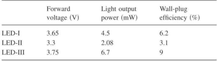
2, the light output power of LED-III is even higher that of LED-I, exhibiting an output power of around 6.7 mW corre- sponding to a WPE of around 9% at an injection current of 20 mA. Table I shows the forward voltage, light output power, and wall-plug efficiency when the LEDs were driven at dc current of 20 mA. Comparing LED-III and LED-I, this marked enhancement of light output or WPE in the LED-III is due to the texture added to the GZO layer, as shown in Fig.
1共b兲. Two reasons account for the increased extraction of photons. First, in the LED-III, photon extraction can occur at the etched GZO sidewall, whereas LED-I has no such side- wall area due to the planar surface of the GZO in LED-I.
Second, the etched GZO surface is rougher than that of the as-deposited GZO surface, as shown in the Fig. 1共c兲. The escape probability of photons generated in the active layer of the LED can be enhanced by increasing the angular random- ization of photons at the roughened surface.4In other words, the combination of the sidewall area and surface roughening on the etched GZO layer could effectively disperse the an- gular distribution of photons in the optical phase space, lead- ing to a larger escape cone in the textured GZO layer over the planar structure. Considering the electrical properties of LED-III and LED-I, although the surface texture performed on the GZO layer should cause a reduction of lateral cross- section area and hence an increase of lateral resistance, only a slight increase in Vf can be obtained indicating that the texture process would not significantly result in a degrada- tion of the electrical property compared to those of GaN-
based LEDs with planar GZO TCL. Although using ITO to serve as the TCL of LED is a well accepted technology, ZnO-based TCLs with high refractive index of around 2.0 would render another advantage when a roughening process is performed on the surface. In other words, since packaged LEDs are generally encapsulated using epoxy with a refrac- tive index of around 1.5, further improvement in light extrac- tion by means of surface roughening performed on ITO TCL would thus be minor because the typical refractive index of an ITO film prepared by our e-beam evaporator is around 1.7.
In conclusion, ITO/GZO and Ni/ Au films were depos- ited on p-type GaN to serve as the TCL. Although the 20 mA forward voltage of LEDs with planar ITO/GZO composite TCL共LED-I兲 is slightly higher than LEDs with Ni/Au TCL 共LED-II兲, the output power of the LED-I is far higher than LED-II. Therefore, the wall-plug efficiency was two times higher than that of LED-II. This improvement could be at- tributed to the fact that the ITO/GZO composite TCL has high transparency and a larger thickness as compared to thin Ni/ Au TCL. The thick ITO/GZO TCL with low lateral resis- tance would also act as the current-spreading layer leading to an enhancement of light extraction. In addition, the thick ITO/GZO TCL with high refractive index could be partially etched away using a HCl solution to form a periodic texture on the GZO layer and thereby result in a further enhance- ment of light extraction efficiency.
1E. F. Schubert, Light-Emitting Diodes, 2nd ed.共Camberidge University Press, New York, 2006兲, p. 185, and references therein.
2H. Kim, D. J. Kim, S. J. Park, and H. Hwang, J. Appl. Phys. 89, 1506 共2001兲 and references therein.
3T. Margalith, O. Buchinsky, D. A. Cohen, A. C. Abare, M. Hansen, S. P.
DenBaars, and L. A. Coldren, Appl. Phys. Lett. 74, 3930共1999兲.
4J. K. Sheu, C. M. Tsai, M. L. Lee, S. C. Shei, and W. C. Lai, Appl. Phys.
Lett. 88, 113505共2006兲 and references therein.
5S. M. Pan, R. C. Tu, Y. M. Fan, R. C. Yeh, and, J. T. Hsu, IEEE Photonics Technol. Lett. 15, 646共2003兲.
6C. H. Lin, D. L. Hibbard, A. Au, H. P. Lee, Z. J. Dong, F. J. Szalkowski, J. Chen, and C. Chen, Mater. Res. Soc. Symp. Proc. 639, G4.8.1共2000兲.
7J. O. Song, K. K. Kim, S. J. Park, and T. Y. Seong, Appl. Phys. Lett. 83, 479共2003兲 and references therein.
8C. J. Tun, J. K. Sheu, B. J. Pong, M. L. Lee, M. Y. Lee, C. K. Hsieh, C. C.
Hu, and G. C. Chi, IEEE Photonics Technol. Lett. 18, 274共2006兲.
9J. K. Sheu, K. W. Shu, M. L. Lee, C. J. Tun, and G. C. Chi, J. Electro- chem. Soc. 154, H521共2007兲, and references therein.
TABLE I. Forward voltage, light output power, and wall-plug efficiency when the LEDs were driven at dc current of 20 mA.
Forward voltage共V兲
Light output power共mW兲
Wall-plug efficiency共%兲
LED-I 3.65 4.5 6.2
LED-II 3.3 2.08 3.1
LED-III 3.75 6.7 9
263511-3 Sheu et al. Appl. Phys. Lett. 90, 263511共2007兲
Downloaded 22 Oct 2009 to 140.116.208.44. Redistribution subject to AIP license or copyright; see http://apl.aip.org/apl/copyright.jsp