Light emitting diodes on Si
Eih-Zhe Liang
a, Ching-Fuh Lin*
a, b, Ting-Wien Su
a, Wu-Ping Huang
a, and Hsing-Hung Hsieh
b aGraduate Institute of Electro-Optical Engineering
bGraduate Institute of Electronics Engineering
National Taiwan University, Taipei, Taiwan, ROC.
ABSTRACT
To extend the usage of silicon as light emitter in optoelectronics, two ways are exploited to overcome its indirect bandgap obstacle. Metal-oxide-semiconductor structures with silicon dioxide (SiO2) nanoparticles as oxide layer
exhibits electroluminescence with 1.5×10⁻⁴
external efficiency at Si bandgap energy. The enhancement in light emission is attributed to carrier concentration due to non-uniformity of oxide thickness. Another approach is to take advantage of direct bandgap materials. Chemically synthesized cadmium sulfide (CdS) nanoparticles are deposited on Si substrate and exhibits electroluminescence corresponding to different process treatment.
Keywords: light emitting diodes, silicon, electroluminescence, silicon dioxide nanoparticle, cadmium sulfide
nanoparticle.
1. INTRODUCTION
Silicon is the most important semiconductor material in electronics industry. However, its importance in optoelectronics is not prominent because indirect-bandgap nature of Si makes it inefficient as a light source. It is a challenging issue for efficient light emitting devices either comprised of silicon or integration of direct bandgap material with silicon. In the past, many efforts had been attempted to overcome such obstacles. These efforts includes conversion of silicon into light-emitting material such porous-silicon-based devices1-3
, nanocrystalline Si 4,5
, Si+
-implanted SiO2 6,7
, deposition of polymer upon Si substrates8
, growth of GaN upon Si substrates9,10
, and so on.
In this work we reported two ways of fabrication of light emitting diodes on silicon. One is to use silicon dioxide (SiO2) nanoparticles as oxide layer in metal-oxide-semiconductor tunneling diode (MOSTD). In silicon, electrons and
holes cannot recombine efficiently due to momentum mismatch. In this structure, or improved MOSTD, we use SiO2
nanoparticles to generate nano-structure to confine electrons and holes so that radiative recombination can be enhanced. We replace traditional oxide layer by SiO2 nanoparticles (particles size 8~12nm)
11
and with its non-uniformity in oxide thickness. Two major effects take place. First, in n-type silicon, holes tunneling through thin region of oxide layer are orders of more than those through thick region. This leads to localized concentration of injected minority carrier (hole). Second, band bending toward the Si/SiO2 interface also depends on oxide thickness. This leads to localized
concentration of accumulated majority carrier (electron). As a result, exciton or electron-hole pairs are more easily formed around thin oxide region than in bulk silicon and radiative recombination rate increases. With KOH wet etch to improve surface condition, external quantum efficiency of electroluminescence (EL) at silicon bandgap edge (wavelength 1.1µm) can be enhanced to 1.5×10⁻⁴
. In addition, frequency response is exploited in characterization of device lifetime. Both nonradiative recombination coefficient and majority carrier density can be extracted from lifetime vs. bias current relation.
Another approach is to disperse cadmium sulfide (CdS) nanoparticles onto silicon and utilize its direct bandgap characteristics for efficient light emission. The advantage of using nanoparticles is its insensitivity of lattice match to the substrate. Severe constrain of lattice match can be relieved. The fabrication of light emitting active layer is simply the spin-coating technique. Carriers to achieve light emission can be supplied by quantum tunneling through surrounding barrier into nanoparticles. By comparison EL spectrum from devices of different process treatment, it is found that there can be significant enhancement of light emission from surface states.
Both ways use silicon as substrate and demonstrate a promising way to monolithically integrate light emitting diodes and conventional electronic circuitry. In this paper, fabrication and characteristics of both light emitting diodes, improved MOSTD and CdS LED, are reported.
* [email protected]; Also with Institute of Electronics Engineering and Department of Electrical Engineering Invited Paper
Light-Emitting Diodes: Research, Manufacturing, and Applications VII, E. Fred Schubert, H. Walter Yao, Kurt J. Linden, Daniel J. McGraw, Editors, 46
2. IMPROVED MOSTD
This section includes the fabrication process of improved MOSTD, emission characteristics and frequency response analysis. Details of applying nanoparticles and wet etch are given. Wet etch time and air exposure day is found to be influential to device performance in electroluminescence. Frequency response is proved to be good tool in investigation of minority carrier lifetime. Both nonradiative coefficient, which is related to interface states, and majority carrier density can be extracted.
2.1 Fabrication of improved MOSTD
The fabrication process steps are as follows. First, native oxide on silicon wafer is removed by buffered oxide etch (BOE) and KOH solution (45%) is subsequently applied to improve surface quality. Prepared SiO2 nanoparticles
solution (5% weight ratio) with feature size 8~11 nm is spin-coated onto surface and baked in oven to remove solvent. The thickness of coated oxide layer is about 150 nm. A thick layer of aluminum is evaporated on wafer backside to form ohmic contact. Conductive silver paint is directly applied on top of the nanoparticles to hold gold wire for top contact. Fig.1 shows scanning-electron microscope photograph of cross-sectional view and schematic of device (inset). Although the thickness of oxide layer seems preventive for tunneling current, it is found metal migration takes place when voltage is applied. Silver particles migrate through the stack of nanoparticles and reach surface until large tunneling current is available from metal to silicon.
Fig. 1: SEM photo of cross-sectional view of improved MOSTD (inset: schematics).
Polish damage is common nonradiative recombination centers for commercially available prime grade silicon wafer. Wet etching solution KOH is used to improve surface quality of silicon wafer and contributes to higher efficiency in emitting light at Si bandgap edge. Commercial 45% KOH is convenient for use. The etching rate of the 45% KOH solution at 35o
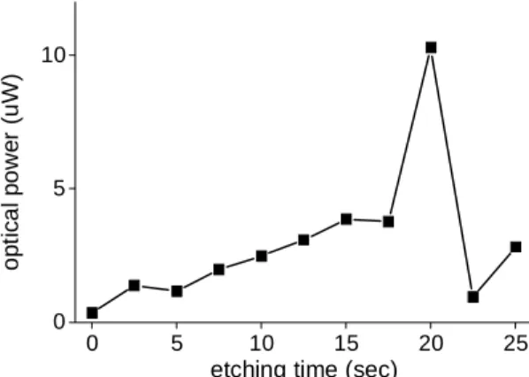
C is about 1 nm/sec. Fig. 2 shows the experiments that KOH etching silicon wafer for 20 seconds can increase the EL intensity for more than 10 times in comparison with the devices without KOH etching (0 second etching time).
Fig. 2: Variation of EL power with KOH etching time
0 5 10 15 20 25 0 5 10 op ti c a l p o we r (u W )
As shown in Fig. 3, EL intensity increases for first few days and then decreases. The reason for increasing efficiency is the formation of native oxide on silicon surface to passivate surface states and to prevent short contact of silver and silicon. Nonradiative recombination is therefore reduced. For overgrown native oxide, high electric field is needed for the same level of tunneling current. Certain region of oxide will breakdown with metal punch-through. Light efficiency reduces and resembles that of first few days.
Fig. 3: Variation of EL power with air exposure days.
2.2 Characteristics of Improved MOSTD
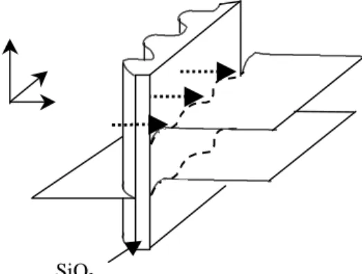
In analysis of improved MOSTD with non-uniform oxide, Fig. 4 shows two-dimensional band diagram. Dashed arrows point to thin oxide regions, where holes tunnel into silicon under positive bias applied to metal. In silicon under thin oxide, electrons accumulate heavily with more surface bending. Spatial confinement of electrons and holes in this nanostructure improves radiative recombination rate. This confinement of both electron and hole is the major reason of high efficiency of light emission. The EL spectrum with origin of phonon-assisted exciton recombination12
is shown in the Fig. 5.
Fig. 4: Two-dimensional band diagram of improved MOSTD on n-type silicon.
Fig. 5: The electroluminescent spectrum correspondent to Si bandgap edge. Ef Ec Ev Si Al energy
z
x SiO2 1000 1100 1200 1300 1400 0.0 0.5 1.0 I=50 mA I=100 mA in te n s ity ( a .u .) wavelength (nm) 0 2 4 6 8 10 0 1 2 3 op ti c a l p o w er (n W)The L-I curve in Fig. 6 shows that EL external quantum efficiency rapidly increases and reaches 1.5x10⁻⁴
for operation current between 20 to 30 mA and slightly drops to 10-4
due to thermal effect. The EL power could be 10μW at the injection current of 100 mA(current density 12.7 A/cm2
). The power is measured only from the periphery of the silver paint pad. Because top contact pad would obstruct a portion of light generated from the device, actual light power might be more than 10μW. If total EL power is included, quantum efficiency will reach 10-3
.
Fig. 6 External quantum efficiency (solid) and output power (dash) vs. injection current relation.
2.3 Frequency response analysis of improved MOSTD
Frequency response with small signal current permits measurement of carrier lifetime under low level bias condition ( < 10A/cm2
) and causes negligible destructive excitation. In analysis of carrier lifetime, nonradiative recombination rate and its coefficient can be determined by the relation between the lifetime and the current bias. The physical reason for the lifetime-bias relation is attributed to extension of accumulation region near surface into silicon bulk region. In improved MOSTD, light is proportional to current in static state condition. Under bias current, the majority carrier concentration is fixed. With modulated current, response time of light is limited by minority carrier recombination rate. To be specific, the rate equation describing minority dynamics is
(1) Minority carrier recombination time is defined asτ =1/(A+Bn) and this parameter is simply frequency response time of modulated light.
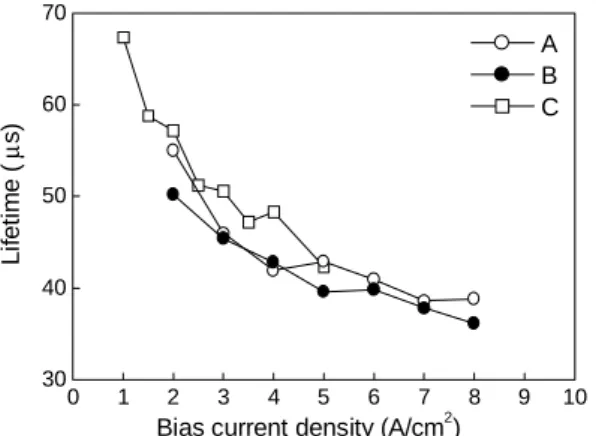
Fig. 7 Measured lifetime of improved MOSTD for different fabrication condition: A, B) normal C) with KOH pre-cure.
Fig. 7 shows the relation between the measured lifetime derived from the frequency response and the bias current. Device A and B are MOSTD fabricated by application of 120nm thick layer of SiO2 nanoparticle. Device C is
fabricated the same way except being pre-treated with KOH wet etch. All devices have metal pad area 0.01cm2
. The 0 20 40 60 80 100 0 10 current (mA) op ti c a l po w e r ( µ W) 0 1x10⁻⁴ e x te rn al qua nt um ef fic ie n c y 0 1 2 3 4 5 6 7 8 9 10 30 40 50 60 70 A B C Li fe ti m e ( µ s)
Bias current density (A/cm2)
p Bn A ed J dt p d
δ
ηδ
δ
= −( + )external light emission efficiency ηext is 5x10
-6, 2x10⁻⁶ and 10-5 (W/A) respectively. With the same light extraction
efficiency ηc and minority carrier injection efficiency ηinj, internal or radiative recombination efficiency ηrec is
proportional to external efficiency because ηext=ηcηinjηrec. Devices with a longer lifetime at low level bias current have
better efficiency and have quite the same lifetime with high level bias current. This suggests that initially lifetime be affected by nonradiative recombination and the reduction of lifetime at increased bias current come from increasing radiative recombination.
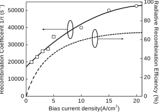
Fig. 8 Fitted recombination coefficient and theoretical recombination efficiency of improved MOSTD
The inverse of lifetime, or recombination coefficientτ−1=A+Bn, under certain level of injection current density J reveals simple relation with carrier density n. However, it lacks theoretical explanation of complex relation between n and J. Observation in Fig. 7 allows us to empirically approach n-J relation by 2
J J
n=β −γ . This saturation behavior of carrier density comes from physical consideration that increasing injection current at high level only extends accumulation depth rather than increases n. Carrier lifetime is related to injection current density by 1 2
J B J B A β γ τ− = + −
as shown by solid line in Fig. 8.
This measurement fitting permits identification of individual contribution of radiative and nonradiative recombination rate. Fitted A is 17185 (sec-1
), Bβ is 320 (sec-1 A-1 cm2 ) and Bγ is 0.718 (sec-1 A-1 cm2 ). However, only nonradiative recombination coefficient can be independently extracted. With typical value of B coefficient as 10-15
cm3
/sec12
, majority carrier density n is in the order of 1019
~1020
cm-3
.
Ratio of radiative recombination rate to overall recombination rate, or radiative recombination efficiency
ηrec=Bn/(A+Bn) can be obtained, as shown by the dash line in Fig. 8. This ratio reaches more than 50% at injection
current density 5A/cm2
, indicating that radiative recombination could be more efficient than nonradiative recombination. This high recombination efficiency comes from selection of high quality silicon wafer for fabrication of MOSTD and using SiO2 nanoparticles for carrier confinement to increase carrier density. Although internal efficiency is high,
external efficiency is limited by low light extraction efficiency due to metal pad and low minority injection efficiency. With frequency response analysis of radiative and nonradiative recombination rate, it is confirmed that internal efficiency of our light emitting diode is very high.
Experiments (frequency response as well as varying efficiency) show that nano-structures in the oxide layer could enhance radiative recombination rate to comparable to Schottky-Read-Hall (SRH) nonradiative recombination rate. This indicates that nonradiative recombination is not the dominant factor, and using SiO2 nanoparticles can enhance silicon EL at the bandgap energy for orders of magnitudes.
3. CdS LED
In this section, light-emitting diode with cadmium sulfide (CdS) nanoparticles as active layer for light emission is reported. It includes preparation of nanoparticles, fabrication of CdS LED, and its spectral characteristics. The emission spectrum is influenced by fabrication process and reflects physical condition of nanoparticles. It is found that there can be significant enhancement of light emission from surface states.
0 5 10 15 20 0 10000 20000 30000 40000 50000 Re c o m b in at io n Co ef fi c e in t 1/ τ (s -1 )
Bias current density(A/cm2)
0 20 40 60 80 100Ra di at iv e Rec o m b in at io n E ffi c ien c y ( % )
3.1 Preparation of CdS nanoparticles
Two kinds of CdS nanoparticles ready for spin-coating purpose are synthesized by modification of Pietro’s method13
. First form is CdS nanoparticle with organic capping. Cadmium acetate dihydrate Cd(CH3COO)2
.
2H2O, 0.80 g, 3.0
mmole) is dissolved in 20 ml mixed solvent of acetonitrile, methanol, and water with volume ratio 1:1:2. Another solution containing disodium sulfide nanohydrate (Na2S
.
9H2O, 0.36 g, 1.5 mmole) and p-hydroxyl thiophenol (0.56 g,
4.4 mmole) in the same solvent system is added into vigorously stirred cadmium acetate solution. The whole system was stirred for 18 hours without light illumination. After removing solvent and purifying by centrifuge, we obtained 0.70 g yellow solid aggregate of CdS nanoparticles capped by p-hydroxyl thiophenol.
Second form of CdS nanoparticle is coated with silica shell. The purpose of preventive use of organic component is to raise the thermal budget of whole fabrication process and increase tolerance with low temperature. The preparation process is as follows. Cadmium acetate dihydrate (Cd(CH3COO)2
.
2H2O, 1.60 g, 6.0 mmole) is dissolved in 32 ml mixed
solvent of acetonitrile and water with volume ratio 1:1. Another solution containing disodium sulfide (Na2S .
xH2O,
x=7~9, 0.58 g, ~2.4 mmole) and (γ-mercaptopropyl) trimethoxysilane (1.41 g, 7.2 mmole) in the same solvent system is added into vigorously stirred solution of cadmium acetate. After being vigorously stirred for 18 hours, the mixture is basified to pH=8.4 with 25% of NH3 aqueous solution. Additional 64 ml of ethanol is added to the mixture. The mixture
is stirred for 48 hours after adding 1.89 g of orthotetraethoxysilane (TEOS). Part of the solvent was removed and precipitation takes place in the mixture. The precipitate is centrifuged for three times and rinsed with deionized water.
The prepared nanoparticle aggregate is redispersable in ethanol or other polar organic solvents. After treated by ultrasonic vibration and percolation, solutions for spin-coating purpose are produced.
The average diameter of the spherical CdS nanoparticles is about 5 nm, as shown in Fig. 9. Compared with the high-temperature synthesizing method by using trioctylphosphine oxygen (TOPO), this room-temperature process is simpler but the particle size distribution is wider.
Fig. 9. TEM image of p-hydroxyl thiophenol capped CdS nanoparticles.
By replacing part of cadmium acetate with manganese acetate, we prepared Mn doped CdS nano- particles with different concentrations of manganese (5%, 10% and 20%, in molar percentage). Through out the experiment, no significant difference of doped and undoped CdS nanoparticles is found under the spectral resolution of our monochromator. To synthesize manganese doped CdS nanoparticles, we have used large molar percentage of Mn, 5 %, 10 % and 20 % respectively in the reaction. However, only trace doping amounts of Mn, 0.08%, 0.05% and 1.10% was detected respectively by ICP-Mass investigations. When the same approach was used to synthesize MnS nanoparticles, a very low yield was obtained. This indicates very low doping content can be made and electroluminescence is less affected by Mn content.
3.2 EL spectrum
We take different post treatments after the nanoparticle film is spin-coated onto silicon substrate. The normal treatment is to remove the solvent without physical change of nanoparticles. Heat treatment is carried out in medium high temperature to explore decomposability of organic passivation and test oxygen cooperation. Oxygen enrichment raises extent of oxygen related surface states. All three conditions show prominent spectral features and can be used to monitor passivation of surface condition.
Origins of electroluminescence of CdS nanoparticle with bulk CdS are schematically shown in Fig. 10. Three exciton levels corresponding to bulk CdS bandgap now change their peak positions of quantum states due to
modification of surface configuration. Modified A free exciton level changes from 508nm to 526.5nm as can be determined in normal treatment of electroluminescence device. Transition level of surface states related to Cd-O termination with peak position of 571.5nm can be observed. This level occurs when passivation of nanoparticle is removed and it has contact with atmosphere, as in heat treatment and oxygen enrichment.
Fig. 10 Energy diagram of CdS nanoparticle.
3.3 Device fabrication of carrier transport
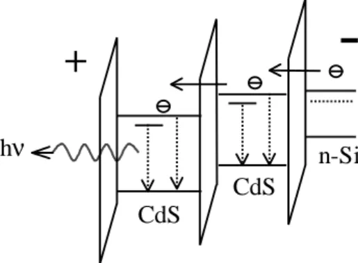
The basic idea about setup of electroluminescence is to use cascade tunneling as injection source. Carriers are supplied by tunneling current through potential barrier of high bandgap material surrounding nanoparticle, as shown in Fig. 11. In our case, the SiO group or organic functional group p-hydroxyl thiophenol serves as the barrier. The choice of substrate to host CdS nanoparticles is silicon due to its surface quality and availability. With different type of injection carriers, depending on n-type or p-type silicon substrate, electrons or holes are emitted from silicon and holes or electrons are emitted from metal deposited. Fermi level of Si in n-type case has to be raised for electrons to tunnel through the potential barrier of p-hydroxyl thiophenol group. Most carriers tunnel into the adjacent nanoparticles. Carriers are expected to recombine within nanoparticles through intrinsic radiative transition or surface-state related transition.
Fig. 11: Schematic of electron transport and transition in the device.
A schematic of CdS-nanoparticle light emitting device is shown in Fig. 12. The fabrication steps are as follows. First, a doped silicon wafer (doping ~1015
cm-3
) is used as substrate. Acetone, methanol, and DI water are used successively for clean procedure. Buffered oxide etch is applied to remove native oxides. The wafer is spin-coated with CdS nanoparticle solutions. Solvents are either removed by evacuation or heat treatment. The thickness of CdS nanoparticle layer can be as large as 500 nm, verified by surface profile scan. In this case, volume density can be very high. Subsequently, both top and bottom metal contacts are made by thermal evaporation. The top semi-transparent contact layer is 10nm gold, and the bottom is 150nm gold. Before the deposition of the Au layer, a 3-nm adhesion layer of chromium had been evaporated for both contacts.
Samples made on n- and p-type Si wafers show different current-voltage curves, as shown in Fig. 13. Both have rectifying current-voltage (I-V) curves, but with opposite polarities. This rectifying effect corresponds to metal-insulator-semiconductor tunneling effect as expected. To be specific, the thin potential barrier of organic functional group and low substrate doping level results in Schottky-diode-like behavior.
CdS
CdS
n-Si
+
h
ν
E
vC
E
xC
E
xB
E
vAE
cE
vB
E
xA
Bulk CdS
E
cwith capping
E
xA’ Surface states
508nm
526.5nm 571.5nm
Fig. 12: Schematic of the CdS nanoparticles EL device on Si wafer.
Fig. 13: I-V curves of devices on n-type and p-type Si.
3.4 Process Effect 3.4.1 Normal process
After spin-coated, the device is placed in a chamber with evacuation at room temperature for 5 minutes to remove ethanol solvents. Both spectra of CdS and CdS doped with Mn are the same, as shown in Fig. 14.
This spectral peak indicates radiative recombination of free exciton in CdS nanoparticles with red-shift due to p-hydroxyl thiophenol groups. The green spectral peak is at 526.5nm (2.355eV), different from bulk CdS A-exciton transition energy, 2.441eV (508nm) at room temperature. Although quantum confinement within the nanoparticles increases exciton energy whenever the particle size decreases14,15
, organic functional group or silicon dioxide matrix can modify the electron configuration within and change ground states significantly. It results in energy red-shift of 86 meV. CdS nanoparticles coated with poly(vinyl alcohol)also show such energy shift in absorption spectrum16
, where photoluminescence at 2.42eV (10K) is observed.
Fig. 14: EL Spectrum of CdS with solvent removed.
Si substrate
450 500 550 600 0.0 0.5 1.0 peak 526.5nm In te n s ity (a .u ) wavelength (nm) -30 -20 -10 0 10 20 30 10-9 10-7 1x10⁻⁵ 10-3 n type Si p type Si cu rr en t( A ) voltage(V)3.4.2. Heat treatment
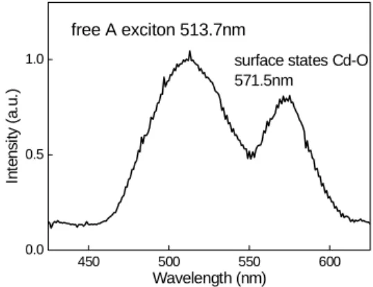
The CdS nanoparticles are spin-coated as described in previous section. These samples are subsequently treated by rapid thermal annealing (RTA) with temperature 425o
C for 5 minutes. The annealing process takes place in nitrogen purge and its purpose is to remove solvent and both test decomposition of organic functional group. Electrical property like I-V curve resembles that in Sec. 3.4.1. As shown in Fig. 15 the emission spectrum consists of two peaks. One is at 513.7nm and the other at 571.5nm. The former peak stands for bulk CdS free A exciton transition.
Fig. 15: The EL Spectrum of CdS particles after heat treatment.
The 571.5nm peak results from the trapped carriers in surface states related to oxygen, Cd-O termination17
. In medium high temperature treatment, decomposition of p-hydroxyl thiophenol group causes oxygen termination with cadmium to occur. It proves p-hydroxyl thiophenol group to be effective overcoat of CdS nanoparticles against oxygen influence. The surface states induce radiative transition as well. The peak magnitude at the spectral lobe is smaller than the magnitude at 513.7 nm, indicating emission from surface states is weaker than that resulted from CdS nanoparticles. However, light power from this sample is generally stronger than that in Sec. 3.4.1. This phenomenon is due to the participation of surface level luminescence, leading to the increase of total light output.
3.4.4 Effect of surrounding oxides
To further study the surface states related to oxygen, we immersed CdS nanoparticles into high oxygen content environment. Two ways are processed. First, the nanoparticle solutions were mixed with spin-on-glass (SOG, Filmtronics 315FX), and the second way, mixed with SiO2 nanoparticles (average diameter of 12 nm, dissolved in
isopropanol). The cleaned, oxide-free silicon substrate is spin-coated and treated by 425o
C to sinter with SiO2 glass. The
similar EL spectrum is found in mixture of CdS nanoparticles with SOG and SiO2 nanoparticles. The peak at 513.7nm
(2.414eV) resembles A free exciton signal of bulk CdS at temperature 65o
C, and the peak at 571.5nm (2.414eV) corresponds to radiative transition due to surface states. The magnitude of total light emission in current setups is ten times stronger than that of unheated samples in Section 3.4.1, under the same carrier injection condition.
Fig. 16: EL spectrum of CdS nanoparticles with oxygen enrichment (solid: Mixed with SOG, dash: Mixed with SiO2 nanoparticles)
450 500 550 600
0.0 0.5
1.0 surface states Cd-O
571.5nm free A exciton 513.7nm In te n s it y ( a .u .) Wavelength (nm) 500 550 600 650 0 20 40
Mixed with SOG
Mixed with SiO2 Nanoparticles
In tensi ty (a. u. ) wavelength(nm)
EL spectrum shown in Fig.16 indicates two mechanisms as shown by the energy diagram in Fig. 10. First, the coalescence of CdS nanoparticles into bulk form results in less broadening spectrum around 513.7 nm. Since the potential barrier of p-hydroxyl thiophenol group disappears due to decomposition, carriers in bulk powders stay for enough time (about 1ns transition lifetime) to recombine radiatively between each tunneling process. Second, relative magnitude of surface-state luminescence is much stronger than that in Sec. 3.4.2. Highly increased concentration of surface state levels, which are supplied by surrounding oxygen termination, contributes to the enhancement of internal quantum efficiency. The magnitude difference between mixture with SOG and SiO2 nanoparticles comes from excess
dangling Si-O bond of the latter case. With the same sintering time, the latter mixture makes more extent of oxygen enrichment.
4. CONCLUSION
We report electroluminescence metal-oxide-semiconductor tunneling diode with improved nanostructure and CdS light-emitting-diode. Both devices are based on silicon. Improved MOSTD that use SiO2 nanoparticles as oxide layer has
external quantum efficiency more than 10-4
. CdS LED uses CdS nanoparticles as active layer and releases constraint of lattice match.
ACKNOWLEDGEMENTS
The authors acknowledge the support from National Science Council, ROC under the contract NSC91-2622-L-002-004, NSC 91-2210-E-002-012 and NSC91-2125-E-002-025.
REFERENCES
1. L. T. Canham, ”Silicon quantum wire array fabrication by electrochemical and chemical dissolution of wafers,” Appl. Phys. Lett. 57, pp.1046-1048 (1990)
2. N. Koshida and H. Koyama, “Visible electroluminescence from porous silicon,” Appl. Phys. Lett. 60, pp. 347-349 (1992)
3. S. Lazarouk, P. Jaguiro, S. Katsouba, G. Masini, S. La Monica, G. Maiello and F. Ferrari, “Stable
electroluminescence from reverse biased n-type porous silicon–aluminum Schottky junction device,” Appl. Phys. Lett. 68, pp.1646-1648 (1996)
4. S. Schuppler et al, “Size, shape, and composition of luminescent species in oxidized Si nanocrystals and H-passivated porous Si,” Phys. Rev. B 52, pp. 4910-4925 (1995).
5. D. B. Geohegan, A. A. Puretzky, G. Duscher and S. J. Pennycook, “Photoluminescence from gas-suspended SiOx
nanoparticles synthesized by laser ablation,” Appl. Phys. Lett. 73, pp.438-440 (1998)
6. L. S. Liao, X. M. Bao, X. Q. Zheng, N. S. Lo and N. S. Min, “Blue luminescence from Si + -implanted SiO 2 films
thermally grown on crystalline silicon,” Appl. Phys. Lett. 68, pp. 850-852 (1996)
7. W. Skorupa, R. A. Yankov, I. E. Tyschenko, H. Frob, T. Bohme, and K. Leo, “Room-temperature, short-wavelength (400–500 nm) photoluminescence from silicon-implanted silicon dioxide films,” App. Phys. Lett. 68, pp.2410-2412 (1996)
8. D. R. Baigent, R. N. Marks, N. C. Greenham, R. H. Friends, S.C. Moratti, and A. B. Holms, “Conjugated polymer light-emitting diodes on silicon substrates,” Appl. Phys. Lett. 65, pp. 2636-2638 (1994)
9. R. Birkhahn amd A. J. Steckl, “Visible emission from Er-doped GaN grown by solid source molecular beam epitaxy,” Appl. Phys. Lett. 73, pp. 1700-1702 (1998)
10. M. Garter, J. Scofield, R. Birkhahn and A. J. Steckl, “Visible and infrared rare-earth-activated electroluminescence from indium tin oxide Schottky diodes to GaN:Er on Si,”Appl. Phys. Lett. 74, pp.182-184 (1999)
11. C. F. Lin, P. F. Chung, M. J. Chen and W. F. Su, “Nanoparticle-modified metal–oxide–silicon structure enhancing silicon band-edge electroluminescence to near-lasing action ,” Optics Lett. 27, pp. 713-715 (2002)
12. M. J. Chen, E. Z. Liang, S. W. Chang and C. F. Lin, “Model for band-edge electroluminescence from metal–oxide– semiconductor silicon tunneling diodes,” J. Appl. Phys. 90, pp. 789-793 (2001)
13. J. G. C. Veinot, M. Ginzburg, and W. J. Pietro, “Surface Functionalization of Cadmium Sulfide Quantum-Confined Nanoclusters. 3. Formation and Derivatives of a Surface Phenolic Quantum Dot,”Chem. Mater. 9, pp.2117-2122, 1997.
B 37, pp.10838-10845, 1988.
15. M.V Rama Krishna, and R.A. Friesner, “Quantum confinement effects in semiconductor clusters,” J. Chem. Phys.
95, pp.8309-8322, 1991.
16. M. Tanaka, J. Qi, and Y. Masumoto, “Optical properties of undoped and Mn2+
-doped CdS nanocrystals in polymer,” J. Crystal Growth 214/215, pp.410-414, 2000.
17. K.J. Hong, T.S. Jeong, C.J. Yoon, and Y.J. Shin, “The optical properties of CdS crystal grown by the sublimation method,” J. Crystal. Growth. 218, pp.19-26, 2000.