五環素有機薄膜電晶體之操作原理與可靠度分析
109
0
0
全文
(2) 五環素有機薄膜電晶體之操作原理與可靠度分析 Device Mechanism and Reliability of Pentacene-based OTFTs 研 究 生:鄭庭軒. Student:Ting-shiuan Cheng. 指導教授:冉曉雯 博士. Advisor:Dr. Hsiao-Wen Zan. 國 立 交 通 大 學 光電工程學系. 光電工程研究所. 碩 士 論 文. A Thesis Submitted to Department of Photonics&Institute of Electro-Optical Engineering College of Electrical Engineering and Computer Science National Chiao Tung University in partial Fulfillment of the Requirements for the Degree of Master in Electro-Optical Engineering June 2006 Hsinchu, Taiwan, Republic of China. 中 華 民 國 九 十 五 年 七 月.
(3) 五環素有機薄膜電晶體之操作原理與可靠度分析 研究生:鄭 庭 軒 . 指導教授:冉 曉 雯 博士. 國立交通大學 光電工程研究所碩士班 摘要 有機薄膜電晶體在面板技術的應用上,由於其具有可彎曲、低溫下製作和 低成本的優勢,所以是非常合適用來製作低成本的電子元件。通常製作有機元件 時會利用表面處理的方式來增加載子的移動率。但卻沒有人針對處理過後原件的 可靠度做分析。因此論文研究利用兩種不同的表面處理過的元件和標準元件在DC 及AC Stress下的變化。 首先,我們設計Gate Four-Probe(GFP)結構來萃取通道內部的電性特性,由 此萃取出薄膜的本質參數。我們分析由Gate Four-Probe(GFP)所得到的電位可發 現 有 機 元 件 的 傳 輸 機 制 與 載 子 漂 移 的 機 制 相 當 類 似 。 之 後 我 們 將 Gate Four-Probe(GFP)結構做在不同表面處理過後的基板上。論文中的元件分為標準和 兩種不同表面處理的元件。標準元件只利用RCA清洗,其他的元件分別用HMDS 或ODMS處理。一開始使用DC Stress,可發現標準元件對於負偏壓的Stress,VTH 漂移量小但是對於正偏壓Vth漂移量大。而有表面處理的元件不管是正負偏壓, Vth漂移量都比標準片大。由Gate Four-Probe(GFP)所分析出的參數顯示pentacene 薄膜並不隨Stress時間有所改變。因此Vth的改變應該是來自於Oxide或是表面處理 layer所貢獻的。利用AC Stress,標準片的Vth漂移量大幅下降顯示出標準片在AC 操作下具有較好的可靠度。但是有處理的HMDS和ODMS的Vth卻仍然有著較大的漂移 量。經HMDS處理後的元件對於頻率和duty-cycle的相關性較大而利用ODMS處理 的元件相關性較小。 I.
(4) Device Mechanism and Reliability of Pentacene-based OTFTs Student: Ting-shiuan Cheng. Advisor: Dr. Hsiao-wen Zan. Institute of Electro-Optical Engineering National Chiao Tung University. Abstract. Due to fixable, low temperature process and low cost, application of organic thin film transistor on flat plane display is very suitable to fabricate low cost device. Usually, surface treatment is used to increase mobility of carrier transport in organic thin film transistor. Until now, without anyone analyze reliability of device which is treated. Therefore this paper studies variation of device with and without surface treatment under different DC and AC stress condition. Firstly, we design Gated-Four-Probe (GFP) structure to extract characteristic of device in channel. Analysis of voltage distribution from Gated-Four-Probe can find that carrier transport mechanism of OTFT is consistent with carrier drift mechanism. Subsequently we fabricate Gated-Four-Probe (GFP) structure on different surface treatment substrate. The devices in this paper are separate to standard and two kinds of surface treatment. Standard device is cleaned by RCA clean and the other devices are treated by HMDS or ODMS. Initially, under DC stress condition we can find threshold voltage shift at positive gate bias stress is larger than at negative gate bias stress. Whether at positive or negative gate bias stress condition, Vth shift of devices II.
(5) with surface treatment are larger than standard devices. The extracted parameters from Gated-Four-Probe (GFP) indicate that pentacene film is not changed with time. Therefore reliability issues lie in the gate insulator or SAM layer degradation. Under AC stress condition, Vth shift of standard devices are obvious decrease. It appears that standard devices have better reliability at AC operation. But Vth shift of devices with HMDS and ODMS still have lager value.. III.
(6) 誌 謝. 首先由衷地感謝指導老師冉曉雯博士在我進修碩士學位期間的殷切鼓勵與 指導。老師孜孜不倦的研究精神,使我獲益匪淺,僅在此獻上最誠摯的謝意。 再則要感謝實驗室的博士班學長國錫學長,士欽學長,政偉學長,在這兩年 的指導與照顧。尤其要感謝士欽學長,在我這兩年的研究生涯中,幫助我度過許 許多多艱辛的時刻。感謝實驗室的同窗夥伴:溥寬、傑斌、全生、貞儀、章祐在 研究上的協助及生活上的關懷。尤其要感謝溥寬這兩年來的互相砥礪,彼此分享 求學路上的喜怒哀樂,使我一路走來不覺寂寞。更要感謝一起從成大來到交大進 修碩士學位的摯友:哲弘,旭信,翰忠,鈞凱等兩年來在製程實驗上的幫助與喜 樂的分享。還要感謝實驗室的學弟妹們:皇維、育敏、廷遠、睿志、爾康、芸嘉、 文馨、德倫、志宏等。感謝你們讓我的研究生涯中,增添了許許多多的歡笑與樂 趣。相當慶幸自己在研究期間有如此多的貴人相助,要感謝的人太多太多,無法 一一列出,謹奉上最真心的感激與祝福。 最後感謝父母親辛勤的陪伴及無悔的付出與照顧,讓我能夠完成碩士學位。. IV.
(7) Contents Chinese Abstract English Abstract. I II IV V VII. 誌謝. Contents Figure Captions. Chapter 1. Introduction 1-1. Overview of Organic TFT Technology. 1. 1-2. Organic semiconducting materials. 2. 1-3. Operating mode of organic thin film transistor. 2. 1-4. Contact resistance in Organic thin film transistors. 4. 1-5. Surface treatment. 5. 1-6. Reliability. 6. 1-7. Motivation. 7. 1-8. Thesis. 7. Chapter 2. Experiment 2-1. 2-2. Overview of Organic TFT Structure. 8. 2-1.1 Shadow mask process. 8. 2-1.2 Surface treatment. 9. Gated four-probe measurements. 9. 2-2.1 Theory of gated four-probe measurements. 2-3. 9. 2-2.2 Gated four-probe structure. 12. 2-2.3 Current-voltage characterization. 12. 2-2.4 Potential measurements. 13. Reliability. .. 2-3.1 Configuration of Measurement Equipments. 14. 2-3.2 Waveform of the AC Signal. 14. 2-3.3 Measurement Methods. 15. V.
(8) Chapter 3. Analysis and Result 3-1. 3-2. 3-3. Gated four-probe analysis. 16. 3-1.1. Current-Voltage characterization. 16. 3-1.2. Potential measurements. 16. 3-1.3. Contact resistance. 17. 3-1.4. Film Resistance Analysis. 18. 3-1.5. Mobility Analysis. 19. DC reliability analysis. 20. 3-2.1. DC bias stress analysis. 20. 3-2.2. Influence of bias stress on thermal Oxide insulator Pentacene-based TFT. 21. 3-2.3. Influence of bias stress on HMDS surface treatment. 22. 3-2.4. Influence of bias stress on ODMS surface treatment. 23. AC reliability analysis. 24. 3-3.1. 24. Without Surface Treatment. 3-3.1.1. Frequency dependence. 24. 3-3.1.2. Duty-cycle dependence. 25. 3-3.2. HMDS Surface Treatment. 26. 3-3.2.1. Frequency dependence. 26. 3-3.2.2. Duty-cycle dependence. 26. 3-3.3. ODMS Surface Treatment. 27. 3-3.3.2. Frequency dependence. 27. 3-3.3.3. Duty-cycle dependence. 28. Chapter 4. Conclusion 4-1 Gated-Four-Probe measurement. 29. 4-2 Reliability of organic thin film transistor. 30. Reference. 31. Figures. 34. VI.
(9) Figure Captions Chapter 1 Fig. 1.1. Molecular structure of (a) sexithiophene and (b) pentacene.. Fig. 1.2 Semilogarithmic plot of mobility vs. year Fig. 1.3. (a) Top contact structure and (b) Bottom contact structure.. Fig. 1.4. Work function of various metals and ionization potential of pentacene.. Fig. 1.5. Schematic view of a bottom-gate thin-film transistor.. Chapter 2 Fig. 2.1. Top view and cross section of the gated-four-probe a-Si:H TFT structure.. Fig. 2.2. show a schematic of the four-probe geometry used to determine film and contact resistance.. Fig. 2.3. Measurement configuration for the organic thin film transistor. Fig. 2.4. Waveform and definition of the AC signal. Chapter 3 Fig. 3.1. Current V.S voltage plots for pentacene thin films with (a) Standard (b) HMDS and (c) ODMS surface treatments.. Fig. 3.2. Potential data and surface plots for devices with Standard, HMDS and ODMS surface treatment. (a), (b) and (c) potential data acquired via the channel potential probes as a function of VG. Shown are the probe data, V1 and V2, along with the extrapolated contact potential VII.
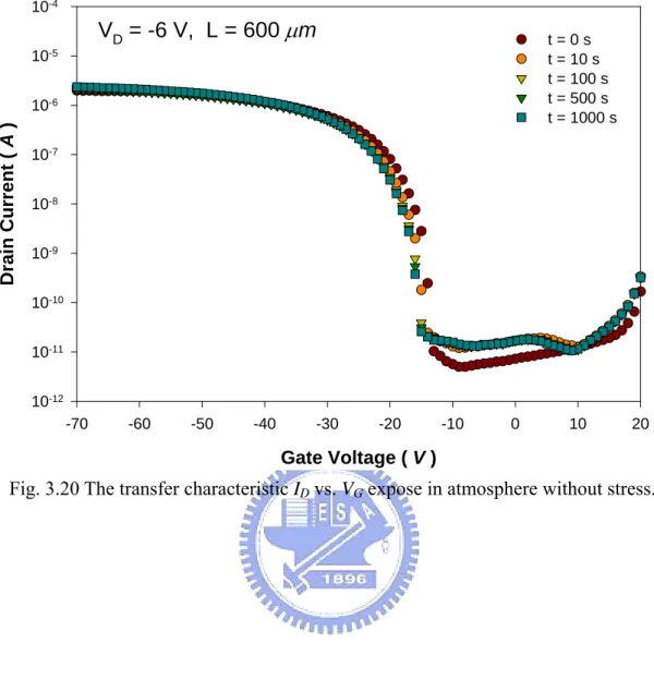
(10) differences at the contacts ∆VS and ∆VD. Fig. 3.3 Potential drops at the source with (a) Standard (b) HMDS and (c) ODMS surface treatments. Fig. 3.4. Potential drops at the drain with (a) Standard (b) HMDS and (c) ODMS surface treatments.. Fig. 3.5. The corresponding energy band of the OTFT operated at different region. Fig. 3.6. Show the film resistances ( RFilm ) and contact resistances ( RD and RS ) as a function of gate voltage for (a) Standard (b) HMDS and (c) ODMS surface treatments top-contacted devices.. Fig. 3.7. illustrate RFilm V.S Channel length at VG = -60V.. Fig. 3.8. illustrate RFilm V.S 1/(VG-VT) for (a) Standard (b) HMDS and (c) ODMS surface treatments top-contacted devices.. Fig. 3.9. (a) and (b) show that mobility which was extracted by gated-four-probe method was not depend on channel length variation.. Fig. 3.10. The transfer characteristic ID vs. VG expose in atmosphere without stress.. Fig. 3.11. Measured transfer curves of a pentacene TFTs deposited on thermal oxide with DC bias stress of -40 V.. Fig. 3.12. Measured transfer curves of a pentacene TFTs deposited on thermal oxide with DC bias stress of 30 V.. Fig. 3.13. Threshold voltage shift vs. bias stress time for positive bias stress of +30 and +40 V, and negative bias stress of -10 and -30 V.. Fig. 3.14. Normalize film mobility of pentacene TFTs after DC bias stress. VIII.
(11) Fig. 3.15. The transfer characteristic ID vs. VG expose in atmosphere without stress.. Fig. 3.16 Measured transfer curves of a pentacene TFTs deposited on HMDS surface treatment with DC bias stress of -40 V. Fig. 3.17 Measured transfer curves of a pentacene TFTs deposited on HMDS surface treatment with DC bias stress of 30 V. Fig. 3.18. Threshold voltage shift vs. bias stress time for positive bias stress of +30 and +40 V, and negative bias stress of -10 and -30 V.. Fig. 3.19. Normalize film mobility of pentacene TFTs after DC bias stress.. Fig. 3.20. The transfer characteristic ID vs. VG expose in atmosphere without stress.. Fig. 3.21 Measured transfer curves of a pentacene TFTs deposited on ODMS surface treatment with DC bias stress of -40 V. Fig. 3.22 Measured transfer curves of a pentacene TFTs deposited on ODMS surface treatment with DC bias stress of 30 V. Fig. 3.23. Threshold voltage shift vs. bias stress time for positive bias stress of +30 and +40 V, and negative bias stress of -10 and -30 V.. Fig. 3.24. Normalize film mobility of pentacene TFTs after DC bias stress.. Fig. 3.25. Pulse voltage was applied to the gate electrode and source and drain were grounded.. Fig. 3.26. The pulse swing region was separated into two parts; one was the ON region, and the other was the OFF region.. Fig. 3.27. Evolution ID-VG characteristic of pentacene-based TFTs deposited on thermal oxide during ON region AC bias-stress with a duty-cycle of IX.
(12) 50% and frequency of (a) 5 Hz (b) 50Hz (c) 200Hz Fig. 3.28. Threshold voltage shift versus effective stress time induced by ON region AC bias-stress with different frequencies.. Fig. 3.29. Mobility variation versus effective stress time.. Fig. 3.30. Evolution ID-VG characteristic of pentacene-based TFTs deposited on thermal oxide during OFF region AC bias-stress with a duty-cycle of 50% and frequency of (a) 5 Hz (b) 50Hz (c) 200Hz.. Fig.3 .31. Threshold voltage shift versus effective stress time induced by OFF region AC bias-stress with different frequencies.. Fig. 3.32. Mobility variation versus effective stress time.. Fig. 3.33. Evolution ID-VG characteristic of pentacene-based TFTs deposited on thermal oxide during (a) ON region (b) OFF region AC bias-stress with a duty-cycle of 25% and frequency of 50Hz.. Fig. 3.34. Threshold voltage shift versus effective stress time induced by ON region AC bias-stress with different duty-cycles.. Fig. 3.35. Mobility variation versus effective stress time.. Fig. 3.36. Threshold voltage shift versus effective stress time induced by OFF region AC bias-stress with different duty-cycles.. Fig. 3.37. Mobility variation versus effective stress time induced by OFF region AC bias-stress with different duty-cycles.. Fig. 3.38. Threshold voltage shift versus effective stress time induced by ON region and OFF region AC bias-stress with different frequencies.. Fig. 3.39. Threshold voltage shift versus effective stress time induced by ON region and OFF region AC bias-stress with different duty-cycles. X.
(13) Fig. 3.40. Evolution ID-VG characteristic of pentacene-based TFTs deposited on HMDS surface treatment during ON region AC bias-stress with a duty-cycle of 50% and frequency of (a) 50Hz (b) 200Hz.. Fig. 3.41. Threshold voltage shift versus effective stress time induced by ON region AC bias-stress with different frequencies.. Fig. 3.42. Mobility variation versus effective stress time induced by ON region AC bias-stress with different frequencies.. Fig. 3.43. Evolution ID-VG characteristic of pentacene-based TFTs deposited on HMDS surface treatment during OFF region AC bias-stress with a duty-cycle of 50% and frequency of (a) 50Hz (b) 200Hz.. Fig. 3.44. Threshold voltage shift versus effective stress time induced by OFF region AC bias-stress with different frequencies.. Fig. 3.45. Mobility variation versus effective stress time induced by OFF region AC bias-stress with different frequencies.. Fig. 3.46. Evolution ID-VG characteristic of pentacene-based TFTs deposited on HMDS during (a) ON region (b) OFF region AC bias-stress with a duty-cycle of 25% and frequency of 50Hz.. Fig. 3.47. Threshold voltage shift versus effective stress time induced by ON region AC bias-stress with different duty-cycles.. Fig. 3.48. Mobility variation versus effective stress time induced by ON region AC bias-stress with different duty-cycles.. Fig. 3.49. Threshold voltage shift versus effective stress time induced by OFF region AC bias-stress with different duty-cycles.. Fig. 3.50. Mobility variation versus effective stress time induced by OFF region XI.
(14) AC bias-stress with different duty-cycles. Fig. 3.51. Threshold voltage shift versus effective stress time induced by ON region and OFF region AC bias-stress with different frequencies.. Fig. 3.52. Threshold voltage shift versus effective stress time induced by ON region and OFF region AC bias-stress with different duty-cycles.. Fig. 3.53. Evolution ID-VG characteristic of pentacene-based TFTs deposited on ODMS surface treatment during ON region AC bias-stress with a duty-cycle of 50% and frequency of (a) 5Hz (b) 50Hz (c) 200Hz.. Fig. 3.54. Threshold voltage shift versus effective stress time induced by ON region AC bias-stress with different frequencies.. Fig. 3.55. Mobility variation versus effective stress time induced by ON region AC bias-stress with different frequencies.. Fig. 3.56. Evolution ID-VG characteristic of pentacene-based TFTs deposited on ODMS surface treatment during OFF region AC bias-stress with a duty-cycle of 50% and frequency of (a) 5Hz (b) 50Hz (c) 200Hz.. Fig. 3.57. Threshold voltage shift versus effective stress time induced by OFF region AC bias-stress with different frequencies.. Fig. 3.58. Mobility variation versus effective stress time induced by OFF region AC bias-stress with different frequencies.. Fig. 3.59. Evolution ID-VG characteristic of pentacene-based TFTs deposited on ODMS treatment during (a) ON region (b) OFF region AC bias-stress with a duty-cycle of 25% and frequency of 50Hz.. Fig. 3.60. Threshold voltage shift versus effective stress time induced by ON region AC bias-stress with different duty-cycles. XII.
(15) Fig. 3.61. Mobility variation versus effective stress time induced by ON region AC bias-stress with different duty-cycles.. Fig. 3.62. Threshold voltage shift versus effective stress time induced by OFF region AC bias-stress with different duty-cycles.. Fig. 3.63. Mobility variation versus effective stress time induced by OFF region AC bias-stress with different duty-cycles.. Fig. 3.64. Threshold voltage shift versus effective stress time induced by ON region and OFF region AC bias-stress with different frequencies.. Fig. 3.65. Threshold voltage shift versus effective stress time induced by ON region and OFF region AC bias-stress with different duty-cycles.. XIII.
(16) Chapter 1 Introduction 1-1 Overview of Organic TFT Technology Organic semiconductors have been known since the late 1940s.[1] However, apart from a very small number of preliminary works on conjugated small molecules [2,3] and polymers[4], the first transistor based on an organic semiconductor was only reported in 1986,[5] with a device made on an electrochemically grown polythiophene film. Polythiophene belongs to the family of the conducting polymers that were discovered in the late 1970s.[6] The inventors of polyacetylene, an archetypal model of conducting polymers, were awarded the Nobel Prize in chemistry in 2000. The possibility of fabricating organic TFT (OTFT) with small conjugated molecules was shown in 1989[7] with sexithiophene, an oligomer of polythiophene made of six thiophene rings linked at alpha position (see Fig. 1.1). Interestingly enough, the organic TFT grew in parallel with another device, the organic light-emitting diode (OLED). As in the case of OTFTs, OLEDs can be made with small molecules[8] or polymers.[9] However, the development of OLEDs has been much faster than that of OTFTs, so that commercial products based on OLEDs are now available on the market, which is not yet the case for OTFTs. In spite of considerable improvements during the last years, the performance of OTFTs remains far beyond that of their inorganic counterpart, except for a-Si:H. For this reason, applications are envisioned where low fabrication costs and large area are of primary importance. These include electronic bar codes and identification tags, and, to a lesser extent, active matrix elements for organic flat panel displays. With this in mind, more and more industrial groups have recently initiated research programs in the field of organic transistors.. 1.
(17) Until recently, much of the research effort has been directed at improving the charge-carrier mobility. Several papers have reviewed this search for better materials and device architecture[10-14].. 1-2 Organic semiconducting materials A number of organic materials such as polythiophene, α- sexithiophene (α-6T) have been investigated for use in field effect transistors (FETs) [15]. Polycrystalline molecular solids such as α-sexithiophene (α-6T) or amorphous/semi-crystalline polymers such as polythiophene or acenes such as pentacene, teracene show the highest mobility [16]. Figure 1.2 shows the evolution of organic materials and the improvement in their mobility over the years [17]. Pentacene based FETs show the high mobility and have been extensively studied. Pentacene is made up of five benzene rings as shown in Fig. 1.1 Pentacene has a sublimation temperature of 300℃. Well ordered pentacene films can be deposited at low temperatures making it suitable for deposition on plastic substrates.. 1-3 Operating mode of organic thin film transistor A thin film transistor is composed of three basic elements: (i) a thin semiconductor film; (ii) an insulating layer; and (iii) three electrodes. Two of them, the source and the drain, are in contact with the semiconductor film at a short distance from one another. The third electrode, the gate, is separated from the semiconductor film by the insulating layer. Figure 1.3(a) and (b) illustrate a widely used configuration of these elements, but as will be shown in the following, there exist several alternative ways of arranging the elements of the device. The Fermi level of gold and HOMO-LUMO levels of pentacene are shown in Fig. 1.4 When a positive voltage is applied to the gate, negative charges are induced at the source electrode. As 2.
(18) can be seen in Fig. 3, the Fermi level of gold is far away from the LUMO level, so that electron injection is very unlikely. Accordingly, no current passes through the pentacene layer, and the small measured current essentially comes from leaks through the insulating layer. When the gate voltage is reversed, holes can be injected from the source to the semiconductor, because the Fermi level of gold is close to the HOMO level. of. pentacene.. Accordingly,. a. conducting. channel. forms. at. the. insulator-semiconductor interface, and charge can be driven from source to drain by applying a second voltage to the drain. For this reason, pentacene is said to be a p-type semiconductor. However, it should be pointed out that this concept differs from that of doping in conventional semiconductors, which can be made either n-type or p-type by introducing tiny amounts of an electron donating or electron withdrawing element. Symmetrically, an organic semiconductor will be said n-type when the source and drain electrodes can inject electrons in its LUMO level, provided electron transport does occur, i.e., electron mobility is not too low. Basically, the thin-film transistor operates like a capacitor. When a voltage is applied between source and gate, a charge is induced at the insulator-semiconductor interface. This charge forms a conducting channel (Fig. 1.5), the conductance of which is proportional to the gate voltage. At low drain voltages, the current increases linearly with drain voltage, following Ohm’s law. When the drain voltage is compared to gate voltage, the voltage drop at drain contact falls to zero and the conducting channel is pinched off. This corresponds to the so-called saturation regime where the current becomes independent of the drain voltage. Below a given threshold, the current increases exponentially. This corresponds to the below-threshold regime. In the above threshold regime, the current becomes proportional to the gate bias, as expected from the above description of the operating mode of the transistor.. 3.
(19) 1-4 Contact resistance in Organic thin film transistors Ongoing efforts to improve the performance of organic thin-film transistors focus on identifying the relation ships between the device structure, film morphology, and charge transport properties. It has been shown that, depending on the device geometry, contact resistances at the source and drain terminals in organic TFTs can be a significant bottleneck to current flow. In the last years, work by a number of research groups has shown that the properties of the source and drain contacts in organic TFTs can have an important effect on the overall devices performance. Jackson, for example, has published a transmission line study of contact resistance in pentacene TFTs [18] showing significant differences in the contact properties for top versus bottom contact devices. In an earlier study, Dimitrakopoulos and co-workers demonstrated that for bottom contact TFTs there is a region of disorder in the pentacene thin film near the contact interface, though the disorder can be mitigated by thiolating the contacts.[19] A powerful alternative to the transmission line method is to map the potential profile across operating OTFTs, as can be done using Kelvin probe force microscopy (KFM).[20–22] Sharp voltage drops, which are observed in the profiles, highlight the resistive bottlenecks to current flow. For example, large contact resistances lead to large voltage drops at the contact-semiconductor interfaces. Dividing the voltage drop by the current yields the contact resistance. Recently Nichols et al.[20] and Puntambekar et al.[21] have reported potential profiling of pentacene OTFTs by KFM. In addition, Burgi et al. have demonstrated potential mapping of polythiophene OTFTs as a function of temperature, which allows a better assessment of the carrier transport mechanisms at the contacts and in the film.[22] 4.
(20) Another contact resistance measurement OTFTs is using the gated four-probe technique, in which the channel potential is sensed at two points between the source and the drain. While this approach does not provide the exquisite detail of a full potential mapping by KFM, it is relatively easy to implement and allows variable-temperature resistance measurements without the need for a UHV-AFM. Four-terminal measurements on a-Si:H TFTs have been extensively reported,[23–26] and recent studies of field-effect transistors based on organic single crystals have also exploited four-probe geometries,[27–30] but so far there have been very few four-terminal measurements on OTFTs. Recently, Yagi et al. reported an initial study of four-terminal pentacene OTFTs.[31]. 1-5 Surface treatment The surface properties such as frictional or abrasion, permeability, insulating properties, wettability and chemical reactivity are strongly dependent on a molecular aggregation state of the surface [32,33]. Therefore, the control of a molecular aggregation state on the film is important to construct a highly functionalized surface. One of the most effective ways of studying surface properties is contact angle measurement. The contact angle is the angle between the tangent to the drop’s profile and the tangent to the surface at the intersection of the vapor, the liquid, and the solid. The contact angle is an index of the wettability of the solid surface. A low contact angle between solid surface water-drop indicates that the surface is hydrophilic and has a high surface energy. On the contrary, a high contact angle means that the surface is hydrophobic and has a low surface energy. The surface free energy was traditionally quantified by contact angle measurements [34,35]. In this work, we fabricated the electrical properties of the OTFTs using 5.
(21) pentacene fabricated by thermal evaporation in high vacuum with the three kinds of dielectric surface treatments; as-prepared (wet cleaning only), hexamethyldisilasane ((CH3)3-Si-O-Si-(CH3)3) (HMDS), and ODMS.. 1-6 Reliability The threshold voltage, and in particular its shift with prolonged application of gate bias stress, is an important parameter for the characterization of thin film transistors. It is well know that bias stress shift the threshold voltage in both organic and inorganic TFTs [38-41]. The shift in threshold voltage foe amorphous and polycrystalline silicon TFTs has been extensively investigated [39, 40]. It effect can arise from low trapping in the dielectric and/pr surface states at the semiconductor/dielectric interface, or the creation of defects in the semiconductor. Recently, bias stress effects have been reported for transistors based on pentacene, polythienylene. vinylene. [42-44]. a-sexithiophene. [45]. poly-9,. 9-dioctyl–fluorene–cobithioph -ene and regioregular-polythiophene [45,46]. In an attempt to understand the physical origin of this instability and the exact location of the trapped charges, several authors have studied the effect using different dielectric materials [42,44] different types of SiO2 , and different surface dielectric treatments [45]. It is well established that ionic movements in thermally grown SiO2 do not occur. Therefore, the data available in the literature suggest that stress in devices using thermally grown SiO2 is related to the properties of the organic semiconductor itself. Recent work has also shown that the bias stress effect can be reversed by band gap light [45] confirming the view that the stress effect is due to trapped charges located within the semiconductor film, near the dielectric interface. Several authors have also reported that the threshold voltage shift is reversible, and that the recovery process can be enhanced by a positive gate bias [41, 47]. 6.
(22) 1-7 Motivation The source/drain contact series resistances not only influence the electrical performance of OTFTs, but also make it difficult to optimize the channel material. To understand the intrinsic performance of OTFT, there is a need for a new structure and/or method which allows exclusion of the effect of source/drain series resistance. OTFT is advantage to make low-cost circuit. But only a few papers were published in reliability field. In order to understand degradation of OTFT, we design three kinds of insulator surface. First, the instability mechanisms of OTFT under DC bias stress have been widely discussed. Because circuits are operated on different frequency, reliability of OTFT under AC stress bias is needed to study. OTFTs treated different methods are measured on different frequency and duty-cycle.. 1-8 Thesis Organization In Chapter 1, we describe the introduction of OTFTs and motivation of the thesis. In Chapter 2, the fabrication, structure and parameter extraction of OTFTs are presented. In Chapter 3, gated-four-probe analysis, DC and AC gate bias stress at OTFTs are investigated. Finally, we describe the conclusion in Chapter 4.. 7.
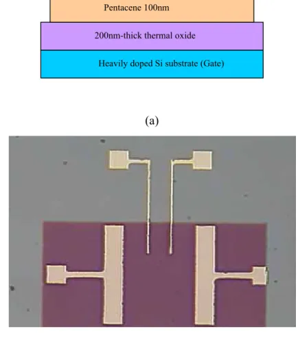
(23) Chapter 2 Experiment 2-1. Overview of Organic TFT Structure. In this study, we fabricated top-contact and bottom-contact structures. The silica substrates consisted of 2000 Å of thermal oxide on p-doped (Boron) silicon wafers. As received, the wafers had an oxide on each side: one side polished and the other unpolished. Below the following sections, we would detail introduce the process of different structures.. 2-1.1 Shadow mask process Step1. Substrate and gate electrode 4-inch P-type heavily-doped single crystal silicon wafer (100) was used as the substrate and the gate electrode. Step2. Gate oxide formation After the initial RCA cleaning, the 2000Å thermally grown SiO2 layer was deposited in furnace. Step3. Pentacene film deposition through shadow mask Pentacene, which was obtained form Aldrich Chemical Company without any purification, was used as an active layer. The deposition was started at a pressure lower than 3×10⁻⁶ torr. The deposition rate was controlled at 0.5Å/s. The temperature we used in depositing pentacene films is 70 oC. We used shadow mask to define the active region of each device. Step4. Au deposition for Top Contact The step formed the Top-Contact in OTFT. We used shadow mask to define top contact of each device. The top electrodes were Au. Au was deposited on the active layer by ULVAC thermal coater at deposition pressure 3×10⁻⁶ torr. The thicknesses of 8.
(24) the metal layer were 500Å. The figure 1.3 (a) show the configuration of structures.. 2-1.2 Surface treatment In order to obtain different surface of oxide layer, we used HMDS and ODMS to modify the surface. HMDS treatment: Before deposited S/D metal or pentacene film, wafer was put into the oven with HMDS steam for 20mins at 150 degree celcius. ODMS treatment: Before deposited S/D metal or pentacene film, wafer was dip in ODMS solution.. 2-2. Gated four-probe measurements. 2-2.1 Theory of gated four-probe measurements The conventional equations describing a-Si:H TFT performance can be derived from the charge control model [37]. In this model the concentration of free carriers, nss, induced into the conducting channel is given by nss =. Ci ⎡⎣VG − VT − VC ( x ) ⎤⎦ q. (1). where Ci is the geometrical capacitance of the gate insulator; VT is the applied gate bias; VG is the effective threshold voltage; VC(x) is the channel potential; and is the electronic charge. In this approximation, the dependence of the charge in the depletion layer on the surface channel potential has been neglected. Based on the gradual channel approximation, the drain current then can be expressed as ⎛ dVC ( x ) ⎞ ⎟ ⎡V − V − VC ( x ) ⎤⎦ W I D = Ci µ FE ⎜ ⎜ dx ⎟ ⎣ G T ⎝ ⎠. (2). where W is the channel width and µ FE is the field-effect mobility. This equation can be rewritten as 9.
(25) ⎛Cµ W dx = ⎜ i FE ⎝ ID. ⎞ ⎟ ⎣⎡VG − VT − VC ( x ) ⎦⎤ dVC ( x ) ⎠. (3). Integration of the above gives ⎛ C µ W ⎞ VD ⎡VG − VT − VC ( x ) ⎤dVC ( x ) dx = ⎜ i FE ⎟ ⎣ ⎦ ID ⎝ ⎠ 0 0. ∫. L. ∫. (4). where L is the channel length and VD is the drain voltage. The above equation leads to the following equation: ⎛W I D = µ FE ⎜ ⎝ L. VD ⎞ ⎞ ⎛ ⎟ Ci ⎜ VG − VT − 2 ⎟ VD for VD ≤ VG − VT ⎠ ⎝ ⎠. (. ). (5). For small VD, this equation can be simplified to G = µ FE Ci (VG − VT ) ⎛. I L ⎞. ⎝. ⎠. (6). D where G ⎜ = WVD ⎟ is the normalized channel conductance.. Equation (6) is traditionally used to extract the field-effect mobility and threshold voltage of a-Si:H TFT operating in a linear region. However, the above derivation does not include the effect of source/drain series resistances. In fact, the source/drain series resistances cannot be ignored in a real a-Si:H TFT. To exclude the voltage drops at source/drain series resistances, the range of integration for in (3) should start from IDRS to ( VD - IDRD ), where RS and RD are series resistances at source and drain terminals, respectively. By assuming RS = RD, the integration of (3) yields V ⎞ ⎛W ⎞ ⎛ I D = µ FE ⎜ ⎟ Ci ⎜ VG − VT − D ⎟ (VD − 2I d RS ) L 2 ⎠ ⎝ ⎠ ⎝. (7). This equation shows that the existence of series resistances make the ID–VG characteristics become nonlinear. If RS is ohmic and is independent of VG, ID, and VD, the intrinsic mobility, threshold voltage, and series resistances can be extracted by least square fit to (7). However, this ideal case is not representative for a-Si:H TFT. In 10.
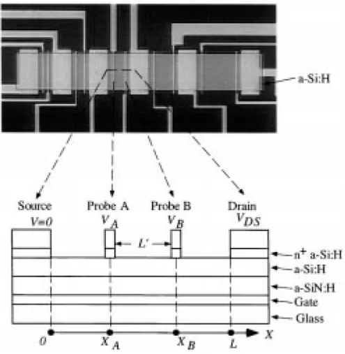
(26) a-Si:H TFT, RS is VG, ID, VD, and source/drain-gate overlap dependent, which makes the extraction of the intrinsic mobility and threshold voltage from (7) difficult. In order to extract intrinsic mobility and intrinsic threshold voltage of a-Si:H TFT, the measurement must exclude the effect of source/drain series resistances. For this reason, we have developed the new gated-four-probe a-Si:H TFT structure described in this letter. Fig. 2.1 shows top view and cross section of this new gated-four-probe a-Si:H TFT structure. It is similar to conventional bottom-gate back-channel-etched a-Si:H TFT but two additional narrow metal electrodes (probe A and probe B) have been added between the source and drain contacts to probe the potential at x = XA and x = XB, respectively. Integration of (3) from x = XA to XB yields. (XB − X A) =. Ci µ FEW ⎡ (V + VA ) ⎤ I D (VB − V A ) ⎢VG − VT − B ⎥ 2 ⎥⎦ ⎣⎢. (8). where VA and VB are the probed channel potential at x = XA and XB, respectively. This equation can be rewritten as ⎛W ⎞ I D = Ci µ FE ⎜ ⎟ (VG ' − VT ) ∆V ⎝ L' ⎠. where ∆V = VB − V A , VG ' = VG −. (9). (VB + VA ) 2. G' = Ci µ FE (VG ' − VT ) ⎛. , and L' = ( X B − X A ) or (10). I L' ⎞. D where G' ⎜ = W ∆V ⎟ is the effective normalized channel conductance. Since probes A ⎝ ⎠. and B sense only the potential but not the current, and there is no current flow through these two probes, VA and VB will represent the true channel potential without being influenced by the source/drain series resistances. The width of probes A and B should be as narrow as possible to avoid influence of these probes on the electrical field 11.
(27) inside the conducting channel.. 2-2.2 Gated four-probe structure Figure 2.2(a) depicts the final bottom gate, inverted-staggered ( top contact ) TFT configuration with the in-channel probes used to measure the channel potential of the operating TFT. Fig. 2.2(b) show a schematic of the four-probe geometry used to determine film and contact resistance. The probes were typically 50 um in width, and penetrate into the channel less than 150 um. The sense probes make up less than 10% of the channel length and penetrate less than 10% of the channel width. The sense probes float at a voltage ( V1, V2 ) corresponding to the channel voltage at the position, thus, the voltage drop at the source and drain electrodes can be determined by extrapolating the channel voltage gradient back to the source and drain. Fig. 2.2(c) illustrates how the channel probe contacts were aligned with the edge of the masked pentacene film. Here, the potential probes only contact the film directly in and near the channel area.. 2-2.3 Current-voltage characterization Electrical characterization was carried out by sweeping the drain voltage ( VD ) at a constant gate voltage ( VG ) or sweeping VG at a constant VD while monitoring the drain current ( ID ) and probe potentials ( V1 ,V2 ). HP 4156 source-measure units were used to apply VD and to measure the source ( IS ) and drain currents. HP 4156 high-impedance ( >1014 Ω ) electrometers were used to monitor V1 and V2 via channel probes and to source VG. All leads except the gate used guarded-shielded triaxial cables instead of shielded coaxial cables to minimize electrical noise and leakage currents. A computer connected to all instrumentation via a general purpose 12.
(28) interface bus running ICS was used to control the operation of all units. The data were exported to and analyzed in ICS. Typical ID–VG parameters used are as follows: for SiO2 dielectric, VD=−3 V, -6 V and -9 V, VG= +20 ~ −70 V, voltage step=1 V, and COX=10 nF/cm2.. 2-2.4 Potential measurements During the standard three-terminal current-voltage measurements, the channel potential was monitored in situ at two points in the channel via the potential probes. At a constant VD, VG was swept and the channel potential was measured at each VG step. Knowing the channel potential at two points, V1 and V2, a linear extrapolation of the potential profile to each contact was performed. From the difference between the applied potential at each contact and the extrapolated potential values for the contacts, the potential drops at the source and drain, △VS and △VD, were calculated according to the following equations: ⎡ (V2 − V1 ) L ⎤ − V ∆VS = ⎢V1 − ⎥ ( L2 − L1 ) 1 ⎦⎥ S ⎣⎢. ,. ⎡ (V2 − V1 ) L − L ⎤ ∆VD = VD − ⎢V2 + ( 2 )⎥ ( L2 − L1 ) ⎣⎢ ⎦⎥. where VS, VD, V1, and V2 are the voltages at the source/drain, and potential probes, respectively. L1, L2, and L are the distances from the source electrode to the first potential probe, the second potential probe, and the drain electrode, respectively. Since we are also interested in examining the potential drop across the film, we define ∆VFilm =. (V2 − V1 ) L ( L2 − L1 ). where △VFilm is the actual drain bias across the film (i.e., the applied drain bias less the drops at the contacts). 13.
(29) 2-3 Reliability 2-3.1 Configuration of Measurement Equipments The measurements used in this study consist of HP 4156A precise semiconductor parameter analyzer, HP41501B pulse generator and HP 16440A SMU/PGU selector. The HP41501B is used to generate the AC pulse signal, including pulse amplitude, frequency, and duty ratio to stress Organic TFTs. After AC signal stress, the OTFT is measured by HP4156A to extract the electrical parameter, including threshold voltage, subthreshold swing, and mobility. Fig. 2.3 illustrates the diagram of the bias stress measurement equipment.. 2-3.2 Waveform of the AC Signal The AC signal used in this study consists of signal amplitudes, frequencies, and duty ratios. We can adjust these parameters and then perform various stress conditions on the gate electrode to realize the instability of Pentacene-based TFTs under different swing regions. Fig. 2-4 shows the waveform of the AC signal. In AC signal, the definition of individual parameter is give as follow:. tc = tvp + t f + tvb + tr f =. (11). 1 tc. D.R. =. (12). (tvp + tr ) (13). tc. Where tc is the signal period, f is the signal frequency and D.R. is the duty ratio. In the waveform of AC signal, VP is the defined as the peak voltage, while Vb is defined as the base voltage. The frequency (f) is equal to 1/tc, where the tc is the signal. 14.
(30) period and the duty ratio is defined a eq. (13). The tvp is the time of peak voltage and the tvb is the time of base voltage. The tf is the falling time. The tr is the rising time. The sum of tvp, tvb, tf, tr is equal to tc.. 2-3.3 Measurement Methods HP 4156A precise semiconductor parameter analyzer was used to perform the stress measurement on the OTFTs and extract the transfer characteristic after DC bias stress. Besides, combining the HP41501B pulse generator with HP 4156A precise semiconductor parameter analyzer, the stress measurement were performed on the TFTs and the transfer characteristics were extracted after AC bias stress. Both of the DC and AC bias stress measurement were performed up to 1000s and interrupted at a specific time to measure the transfer curves at the drain-to-source voltage (Vds) of 6V ( in linear region ). At last, the electrical characteristics of OTFTs were extracted by an HP 4156A electrical analyzer.. 15.
(31) Chapter 3 Analysis and Result 3-1 Gated four-probe analysis 3-1.1 Current-Voltage characterization We fabricated three differential oxide interfaces of organic thin film transistors. The standard devices were only cleaned by RCA clean. The other devices were treated by HMDS and ODMS. For most devices, transfer curves were taken in 1 V gate steps from -20 V up to +70 V. Figure 3.1 (a), (b) and (c) show that transfer curves of devices with different surface treatments. The curves obtained for all other OTFTs which had same oxide interface were similar to that observed for this device and were not shown. For different surface treatments, the threshold voltages of devices were different. The threshold voltage of devices with surface treatment were shift to more negative. Because the different surface treatments make oxide interface to have different surface state, like surface energy, roughness and trap density of states. Therefore, we used gated-four-probe structure to extract the mobility of devices and to map the potential in the channel.. 3-1.2 Potential measurements Figures 3.2(a), 3.2(b) and 3.2(c) represent plots of measured channel potentials V1 and V2 and calculated ∆VS and ∆VD as a function of VG for standard, HMDS and ODMS surface treatment devices. Here, the potential data are truncated just after Von, where the device initially begins to conduct. Before this point, the voltage probes measure potentials that are outside the range of the applied source or drain biases. We believe that these results from static charge buildup on the pentacene film surface and in the cables of the measurement system while the film is relatively nonconductive. 16.
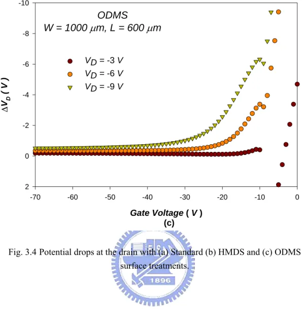
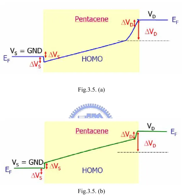
(32) As soon as an appreciably conducting channel is established, the probes report potentials characteristic of the channel. Data on standard, HMDS and ODMS show the same trends. In chapter 2-4-2, we had explained how extract the potential drops at the source and drain, ∆VS and ∆VD. The potential drops at the source and drain, △VS and △VD, were calculated according to the following equations: ⎡ (V2 − V1 ) L ⎤ − V ∆VS = ⎢V1 − ⎥ ( L2 − L1 ) 1 ⎥⎦ S ⎢⎣. ,. ⎡ (V2 − V1 ) L − L ⎤ ∆VD = VD − ⎢V2 + ( 2 )⎥ ( L2 − L1 ) ⎢⎣ ⎥⎦. Figure 3.3 (a), (b) and (c) show that the potential drops at the source, ∆VS with different surface treatment. In above figures, we found that source side voltage drop turns from positive value to negative value. Figure 3.4 (a), (b) and (c) show that the potential drops at the drain, ∆VD with different surface treatments. The Figure 3.5 (a), (b) and (c) show that the potential maps of channel from VG=VON to VG=-70V. The corresponding energy band was depicted in Fig. 3.4. In Fig. 3.5(a), hole injected from source electrode face a barrier due to the difference of metal work function and the pentacene HOMO band. When gate bias is applied as in Fig. 3.5(b), the injection barrier is reduced and even removed when ∆VS becomes negative. In addition to standard devices, devices with HMDS and ODMS treatment had same behavior.. 3-1.3 Contact resistance With the knowledge of the total current flowing through the device and the potential drops across the film and contacts, the resistance of the source contact, drain contact, and the film can be calculated using Ohm’s Law, Ri=∆Vi / ID, where i is S, D, and Film. Therefore we can obtain ∆RS , ∆RD and RFilm by RFilm =. (V2 − V1 ) L I D ( L2 − L1 ) 17.
(33) ⎡ (V2 − V1 ) L ⎤ − V ⎢V1 − ⎥ ( L2 − L1 ) 1 ⎦⎥ S ⎢ RS = ⎣ ID. ,. ⎡ (V2 − V1 ) L − L ⎤ VD − ⎢V2 + ( 2 )⎥ ( L2 − L1 ) ⎢⎣ ⎥⎦ RD = ID. Figures 3.6(a) 3.6(b) and 3.6(c) for Standard, HMDS and ODMS top-contacted devices, respectively, show plots of resistance as a function of gate voltage. Initially, at low VG, the film resistances ( RFilm ) and contact resistances ( RD and RS ) all begin at large values of resistance with RD much larger than RS. As VG is increased, the resistance of both the film and contacts decrease rapidly and finally saturate. Note that the data at low VG (less than VT) could be misleading because when ∣VG-VT∣ < ∣VD∣, the device is in saturation and pinch off occurs. The depletion region associated with pinch-off introduces a high-resistance region near the drain electrode, and the potential profile across the film is not linear. The gated-four-probe technique presented here does not decouple the resistance due to the saturation-induced depletion region from the contact resistance.. 3-1.4 Film Resistance Analysis The figures 3.7 show that the dependence of the normalized film resistance on channel length at VG = -60 V with VD = -6 V. Obviously film resistance changed with channel length increasing. When devices were operated in linear region, the drain current ID can be written as ID =. W µ C (V − V ) V L FE ox G T D. Therefore the film resistance can be induced as RFilm =. L. W µ FE Cox (VG − VT ). 18.
(34) Above equation was induced by J = σ E = qvn = qµ nE (current drift equation). 1. In figure 3.8 (a) (b) and (c), we found that RFilm depend on V − V . According to ( G T) current drift equation, we can demonstrate the drift mechanism which was suitable for organic thin film transistor.. 3-1.5 Mobility Analysis In general, extracted mobility of devices which were fabricated simultaneously has different value at different channel length and drain bias. For the gated-four-probe measurement, the mobility µFE had been extracted using the equations: GM =. W C µ (V − V ) L12 ox FE 1 2. µ FE =. GM × L12 WCox (V1 − V2 ). Where the GM is the channel conductivity, Cox is the gate insulator capacitance per unit area, and V1 and V2 are the potentials measured by the voltage probing electrodes. L12 is the length of distance between two probes. And the µ0 is extracted by a general method from linear region. Figure 3.9 (a) and (b) show that mobility which was extracted by gated-four-probe method was not depend on channel length variation. The mobility was not affected by parasitic resistance. Therefore gated-four-probe method was convenient to monitor the variation of pentacene film.. 3-2 DC reliability analysis One of the most important stability issues in organic transistors is the shift in the threshold voltage upon applying a bias to the gate electrode, so-called stressing. The shift in threshold voltage induced by gate bias stress has been well studies in 19.
(35) amorphous silicon [48], and has recently been studied in pentacene-based TFTs [49]. Gate bias stress in amorphous silicon TFTs is ascribed to several mechanisms including: charge trapping in the insulator, surface state creation at the semiconductor/insulator interface, or creation of metstable traps within the semiconductor [50]. Gate bias stress in OTFTs has been studied very little. In this study, we fabricated three kinds of interface of pentacene-based devices. These devices were treated by HMDS or ODMS. On the other hand, we also fabricated standard devices which were clean only RCA clean. Three kinds of devices were given different bias stress to observe the difference after stress. The experiment was divided into two parts. One was DC (direct current) stress, and the other was the AC (alternating current) stress.. 3-2.1 DC bias stress analysis Under DC stress, the gate bias stress measurements were performed in atmosphere and darkness on Pentacene-based TFTs on SiO2 substrates with Au contacts. The stress gate voltage were -40V, -60V (negative bias stress), 30V, and 40V (positive bias stress), respectively. Between transfer curves, the device was stressed for a time interval (t) at a fixed gate voltage (VG,Bias) with a drain voltage of VD = 0 V. HP 4156A precise semiconductor parameter analyzer was used to perform the stress measurement on the transfer characteristics after DC stress. Typically, transfer curves were taken from, VG = +20 to -70 V at 1V steps. Between transfer curves, the device was stressed for a time interval (t) at a fixed gate voltage (VG,Bias ) with a drain voltage of VD = 0 V. 20.
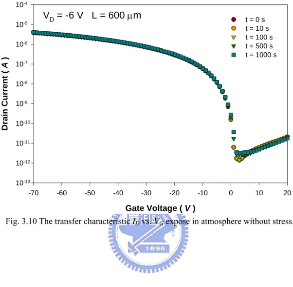
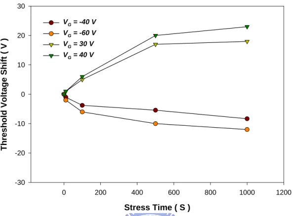
(36) 3-2.2 Influence of bias stress on thermal Oxide insulator Pentacene-based TFT First, we measured the electric characteristics of OTFTs without any stress in the atmosphere as the control sample. The transfer characteristic ID vs. VG was illustrated in Fig. 3.10. We can find the threshold voltage was not shift with time increase. Fig. 3.11 show a series of transfer curves at t = 0, 10, 100, 500 and 1000 sec, between which VG, Bias = -40 V (negative bias stress). The arrow in Fig.3.11 indicates the increase of stress time from 0 to 10, 100, 500, and 1000 sec, respectively, and these cause a shift in threshold voltage of about -2V. Fig. 3.12 show a series of transfer curves at t = 0, 10, 100, 500 and 1000 sec, between which VG, Bias = +30 V (positive bias stress), respectively. The same, in Fig. 3.12., the arrow indicates the increase of stress time and these cause a shift in threshold voltage of about 9V. Fig. 3.13 plots the shift of the threshold voltage for different stress times, and includes data for negative gate bias stress and positive gate bias stress at different stress levels. Positive bias stress moves the threshold voltage towards positive voltages, whereas for negative stress the threshold voltage shift towards negative threshold voltage. The threshold voltage increase over time but with a nonlinear dependence, and the shift increases with a nonlinear dependence, and the shift increase with stress bias. There is more pronounced shift of threshold voltage for positive gate voltages, but the form of the data for negative bias is otherwise rather similar. Fig. 3.14 shows the normalize film mobility which extracts from gated-four-probe measurement. The film mobility of penetacene-based TFTs after DC bias stress was not change conspicuously. Negative gate bias stress cause a negative threshold shift and positive gate bias stress cause a positive threshold shift, while the 21.
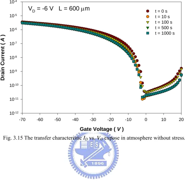
(37) mobility remain unchanged. This effect was assigned to trapping of charges at the interface to the insulator, or in the insulator itself. In our device, Electron trapping is more pronounced than hole trapping. Similar result were previously obtained on amorphous silicon thin-film transistors and attributed to charge injection into the SiO2 insulator [51].. 3-2.3 Influence of bias stress on HMDS surface treatment The same, we measured the electric characteristics of OTFTs without any stress in the atmosphere as the control sample. The transfer characteristic ID vs. VG was illustrated in Fig. 3.15. Fig. 3.16 shows a series of transfer curves at t = 0, 10, 100, 500 and 1000 sec, between which VG, Bias = -40 V (negative bias stress). The arrow in Fig.3.16 indicates the increase of stress time from 0 to 10, 100, 500, and 1000 sec, respectively, and these cause a shift in threshold voltage of about -8V. Fig. 3.17 shows a series of transfer curves at t = 0, 10, 100, 500 and 1000 sec, between which VG, Bias = +30 V (positive bias stress), and these cause a shift in threshold voltage of about 12V. Fig. 3.18 plots the shift of the threshold voltage for different stress times, and includes data for negative gate bias stress and positive gate bias stress at different stress levels. Fig. 3.19 shows the normalize film mobility which extracts from gated-four-probe measurement. The film mobility of penetacene-based TFTs after DC bias stress was not change conspicuously. Reliability issues lie in the HMDS layer degradation. HMDS may enhance the degradation since HMDS is more capable of trapping carriers than SiO2.. 22.
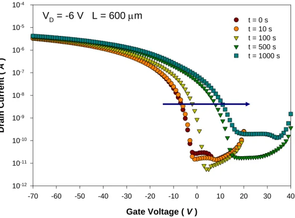
(38) 3-2.4 Influence of bias stress on ODMS surface treatment We measured the electric characteristics of OTFTs without any stress in the atmosphere as the control sample. The transfer characteristic ID vs. VG was illustrated in Fig. 3.20. Fig. 3.21 and Fig. 3.22 show a series of transfer curves at t = 0, 10, 100, 500 and 1000 sec, between which VG, Bias = -40 V (negative bias stress), +30 V (positive bias stress), respectively. The arrow in Fig. 3.21 and Fig. 3.22 indicates the increase of stress time from 0 to 10, 100, 500, and 1000 sec, respectively. Fig. 3.23 plots the shift of the threshold voltage for different stress times, and includes data for negative gate bias stress and positive gate bias stress at different stress levels. Positive bias stress moves the threshold voltage towards positive voltages, whereas for negative stress the threshold voltage shift towards negative threshold voltage. Fig. 3.24 shows the normalize film mobility which extracts from gated-four-probe measurement. The film mobility of penetacene-based TFTs after DC bias stress was not change conspicuously. Reliability issues lie in the ODMS layer degradation.. 3-3 AC reliability analysis Under AC stress, pulse voltage was applied to the gate electrode and source and drain were grounded, which is shown in Fig. 3.25. A rectangular pulse was used with various frequencies and duty cycles to observe the devices degradation under different operating regions. The signal frequencies ranged from 5Hz to 200Hz, and the duty -cycle ranged from 50% to 25%. The pulse swing region was separated into two parts; one was the ON region, and the other was the OFF region as shown in Fig. 3.26. The ON region means pulse swing over threshold voltage where the channel region was 23.
(39) formed. The OFF region means pulse swing under threshold voltage where the channel region was fully depleted. At last, the electrical characteristics of OTFTs were extracted by an HP 4156A electrical analyzer. The field effect mobility is extracted from gated-four-probe measurement. The Vth shift is defined as the difference between Vth2 and Vth1, where Vth1 is the threshold voltage before stress and Vth2 is the threshold voltage after stress.. 3-3.1 Without Surface Treatment 3-3.1.1 Frequency dependence In order to observe degradation of the device at the ON region stress and the OFF region stress, various frequencies range from 5Hz to 200Hz were applied at a fixed tr = tf = 100ns and D.R = 50%. Fig. 3.27 shows a series of transfer curves (ID-VG) at 0, 100, 500, 1000 sec, between which VG (AC bias) = -40 V was applied at various frequencies. Fig 3.28 shows the threshold voltage shift versus effective stress time under ON region AC bias-stress for different frequency conditions. The effective stress time is the accumulated time when gate voltage is high. For the ON region bias-stress, AC and DC bias-stress induce a similar evolution of ID-VG characteristic and the threshold voltage shift dose not depends apparently on AC bias frequency. The mobility variation under the ON region at various frequencies was shown in Fig.3.29. The mobility variation is expressed as the ratio of stressed mobility (μstress) to initial mobility (μinitial). Fig 3.29 indicates the mobility was not changed under ON region stress. Fig. 3.30 shows a series of transfer curves (ID-VG) at 0, 100, 500, 1000 sec, between which VG (AC bias) = 30 V was applied at various frequencies. Fig 3.31 shows the threshold voltage shift versus effective stress time under OFF region AC bias-stress for different frequency conditions. For the OFF region AC bias-stress, threshold voltage shift is slightly smaller than that for DC bias-stress and depends 24.
(40) weekly on AC bias frequency. The mobility variation under the OFF region at various frequencies was shown in Fig. 3.32. Like the ON region AC bias stress, the mobility is almost constant under OFF region AC bias-stress.. 3-3.1.2 Duty-cycle Dependence Fig. 3.33 shows a series of transfer curves (ID-VG) at 0, 100, 500, 1000 sec, between which VG (AC bias) = -40 V and +30 V were applied at duty-cycle of 25%, respectively. Fig 3.34 shows the threshold voltage shift versus effective stress time under ON region AC bias-stress for different duty-cycles conditions. Fig. 3.35 shows the mobility variation under the ON region AC bias stress at various duty-cycles. Fig 3.36 shows the threshold voltage shift versus effective stress time under OFF region AC bias-stress for different duty-cycles conditions. Fig. 3.37 shows the mobility variation under the OFF region AC bias stress at various duty-cycles. Fig. 3.38 gives a summary of NO region and OFF region AC bias stress measurements at different frequencies. Fig. 3.39 shows the threshold voltage shift versus effective stress time under both ON region and OFF region AC bias stress for different duty-cycle conditions. It was reported previously that detrapping during pulsed operation can explain the smaller threshold voltage shift induced by DC bias stress. The detrapping mechanism can be applied to OTFTs if the electrical instability mechanism is mainly associated with the charge-trapping in the gate insulator. During the OFF-cycle of the AC bias-stress, some of the trapped charge which is not deeply trapped could be relaxed from the trap centers.. 25.
(41) 3-3.2 HMDS Surface Treatment 3-3.2.1 Frequency dependence Fig. 3.40 shows the evolution of ID-VG characteristic of HMDS surface treatment pentacene-based TFTs during ON region AC bias stress with a duty-cycle of 50% at various frequencies. The arrow in Fig. 3.40 indicates the increase of stress time from 0 (unstressed) to 100, 500, 1000 sec, respectively. Fig 3.41 shows the threshold voltage shift versus effective stress time under ON region AC bias-stress for different frequency conditions. For the ON region AC bias-stress, the threshold voltage shift has strong frequency dependence, the greater the magnitude of threshold voltage shift. The mobility variation under the ON region at various frequencies was shown in Fig. 3.42. Fig 3.42 indicates the mobility was almost constant under ON region stress. Fig. 3.43 show the evolution of ID-VG characteristic of HMDS surface treatment pentacene-based TFTs during OFF region AC bias stress with a duty-cycle of 50% at various frequencies. The arrow in Fig. 3.43 indicates the increase of stress time from 0 (unstressed) to 100, 500, 1000 sec, respectively. Fig 3.44 shows the threshold voltage shift versus effective stress time under OFF region AC bias-stress for different frequency conditions. The mobility variation under the OFF region at various frequencies was shown in Fig. 3.45. Like the ON region AC bias-stress, the threshold voltage shift also has strong frequency dependence and the mobility was not changed at different frequency condition.. 3-3.2.2 Duty-cycle Dependence Fig. 3.46 shows a series of transfer curves (ID-VG) at 0, 100, 500, 1000 sec, between which VG (AC bias) = -40 V and +30 V were applied at duty-cycle of 25%, respectively. Fig 3.47 shows the threshold voltage shift versus effective stress time under ON region AC bias-stress for different duty-cycles conditions. Fig. 3.48 shows 26.
(42) the mobility variation under the ON region AC bias stress at various duty-cycles. Fig 3.49 shows the threshold voltage shift versus effective stress time under OFF region AC bias-stress for different duty-cycles conditions. Fig. 3.50 shows the mobility variation under the OFF region AC bias stress at various duty-cycles. Fig. 3.51 gives a summary of NO region and OFF region AC bias stress measurements at different frequencies. Fig. 3.52 shows the threshold voltage shift versus effective stress time under both ON region and OFF region AC bias stress for different duty-cycle conditions.. 3-3.3 ODMS Surface Treatment 3-3.3.1 Frequency dependence Fig. 3.53 shows a series of transfer curves (ID-VG) at 0, 100, 500, 1000 sec, between which VG (AC bias) = -40 V was applied at various frequencies. Fig 3.54 shows the threshold voltage shift versus effective stress time under ON region AC bias-stress for different frequency conditions. For the NO region bias-stress, AC and DC bias-stress induce a similar evolution of ID-VG characteristic and the threshold voltage shift dose not depends apparently on AC bias frequency. The mobility variation under the ON region at various frequencies was shown in Fig. 3.55. Fig 3.55 indicates the mobility is almost constant under ON region stress. Fig. 3.56 shows a series of transfer curves (ID-VG) at 0, 100, 500, 1000 sec, between which VG (AC bias) = 30 V was applied at various frequencies. Fig 3.57 shows the threshold voltage shift versus effective stress time under OFF region AC bias-stress for different frequency conditions. The mobility variation under the OFF region at various frequencies was shown in Fig. 3.58. Like the ON region AC bias stress, the mobility is almost constant under OFF region AC bias-stress.. 27.
(43) 3-3.3.2 Duty-cycle Dependence Fig. 3.59 shows a series of transfer curves (ID-VG) at 0, 100, 500, 1000 sec, between which VG (AC bias) = -40 V and +30 were applied at duty-cycle of 25%, respectively. Fig 3.60 shows the threshold voltage shift versus effective stress time under ON region AC bias-stress for different duty-cycles conditions. Fig. 3.61 shows the mobility variation under the ON region AC bias stress at various duty-cycles. Fig 3.62 shows the threshold voltage shift versus effective stress time under OFF region AC bias-stress for different duty-cycles conditions. Fig. 3.63 shows the mobility variation under the OFF region AC bias stress at various duty-cycles. Fig. 3.64 gives a summary of NO region and OFF region AC bias stress measurements at different frequencies. Fig. 3.65 shows the threshold voltage shift versus effective stress time under both ON region and OFF region AC bias stress for different duty-cycle conditions.. 28.
(44) Chapter 4 Conclusion 4-1. Gated-Four-Probe measurement In this study, we successfully fabricate gated-four-probe structure to extract. parameters of organic thin film transistor. Analyses of devices with different surface treatments show the variation of voltage drop at source/drain. Although devices have three kinds of surfaces, different surfaces do not affect the voltage drop at source/drain. From Fig. 3.5, we understand that the injection barrier is reduced and even removed when VG is large enough. In section 3-1.4, we found that RFilm which 1. was extracted by gated-four-probe depends on V − V . ( G T). 4-2. Reliability of organic thin film transistor We used gated-four-probe structure to monitor variation of devices with. different surface treatments during stress. First, devices were operated under DC stress. The standard devices which were stressed under negative voltage have smaller value of Vth shift than under positive voltage. The devices with surface treatment show that HMDS and ODMS may enhance the degradation since HMDS and ODMS are more capable of trapping carriers than SiO2. Subsequently, devices were operated under AC stress. The Vth shift values of standard devices which are stressed by positive voltage are obviously decreased. But devices with HMDS treatment strongly depend on frequency and duty-cycle, the Vth shift of devices is still lager than standard ones. Although the Vth shift of devices with ODMS treatment are still lager than standard ones, the shift values weakly depend on frequency and duty-cycle. All data of devices were measured by gated-four-probe structure, variation of devices were monitored. The extracted parameters of devices show that pentacene film is not degraded. Therefore, the Vth shift of devices may be come from variation of SAM 29.
(45) layer. The different results of devices with different surface treatment may be due to that chain length or polarization of SAM materials. Polarized SAM can selectively trap charges. For polarized SAM, opposite electric filed is needed to release the trap charges.. 30.
(46) References. [1]. M. Pope and C.E. Swenberg, Electronic Processes in Organic Crystals and Polymers (Oxford University Press, New York, 1999). [2]. D.F. Barbe and C.R. Westgate: Surface state parameters of metal-free phthalocyanine single crystals. J. Phys. Chem. Solids 31, 2679 (1970). [3]. M.L. Petrova and L.D. Rozenshtein: Field effect in the organic semiconductor chloranil. Fiz. Tverd. Tela (Soviet Phys. Solid State) 12, 961 (1970). [4]. M.L. Petrova and L.D. Rozenshtein: Field effect in the organic semiconductor chloranil. Fiz. Tverd. Tela (Soviet Phys. Solid State) 12, 961 (1970). [5]. F. Ebisawa, T. Kurokawa, and S. Nara: Electrical properties. of. polyacetylene-polysiloxane interface. J. Appl. Phys. 54, 3255 (1983). [6]. A. Tsumura, K. Koezuka, and T. Ando: Macromolecular electronic device: Field-effect transistor with a polythiophene thin film. Appl. Phys. Lett. 49, 1210 (1986). [7]. H. Shirakawa, E.J. Louis, A.G. MacDiarmid, C.K. Chiang, and A. Heeger: Synthesis of electrically conducting organic polymers: Halogen derivatives of polyacetylene, (CH)x. J. Chem. Soc. Chem. Commun. 00, 578 (1977). [8]. G. Horowitz, D. Fichou, X.Z. Peng, Z.G. Xu, and F. Garnier: A field-effect transistor based on conjugated alpha-sexithienyl. Solid State Commun. 72, 381 (1989). [9]. C.W. Tang and S.A. van Slyke: Organic electroluminescent diodes. Appl. Phys. Lett. 51, 913 (1987). [10]. J.H. Burroughes, D.D.C. Bradley, A.R. Brown, R.N. Marks, K. Mackay, R.H. Friend, P.L. Burns, and A.B. Holmes: Lightemitting diodes based on conjugated polymers. Nature 341, 539 (1990). [11]. H.E. Katz: Organic molecular solids as thin film transistor semiconductors. J. Mater. Chem. 7, 369 (1997). 16. A.R. Brown, C.P. Jarrett, D.M. de Leeuw, and M. Matters: Fieldeffect transistors made from solution-processed organic semiconductors. Synth. Metal 88, 37 (1997). [12]. F. Garnier: Thin-film transistors based on organic conjugated semiconductors. Chem. Phys. 227, 253 (1998). [13]. G. Horowitz: Organic field-effect transistors. Adv. Mater. 10, 365 (1998). [14]. C.D. Dimitrakopoulos and P.R.L. Malenfant: Organic thin film transistors for large area electronics. Adv. Mater. 14, 99 (2002). [15]. L. Torsi, A. Dodabalapur, L. J. Rothberg, A. W. P. Fung, H.E. Katz, 31.
(47) “Performance Limits of Organic Transistors”, Science, 1996, P 1462. [16]. H. E. Katz, C. Kloc, V. Sundar, J. Zaumseil, A. L. Briseno, Z. Bao, “Field-Effect Transistors made from Macroscopic Single Crystals of Teracene and Related Semiconductors on Polymer Dielectrics”, Journal of Material Research, Vol. 19, No. 7, Jul 2004, P 1995 - 1998. [17]. C. D. Dimitrakopoulos, D. J. Mascaro, “Organic Thin-Film Transistors: A Review of Recent Advances”, IBM Journal of Research and Development, Vol. 45, No. 1, Jan 2001, P 11 - 27. [18] 1P. V. Necliudov, M. S. Shur, D. J. Gundlach, and T. N. Jackson, J. Appl. Phys. 88, 6594 ~2000; D. J. Gundlach, L. Jia, and T. N. Jackson, IEEE Electron Device Lett. 22, 571 ~2001; P. V. Necliudov, M. S. Shur, D. J. Gundlach, and T. N. Jackson, Solid-State Electron. 47, 259 ~2003; H. Kluak, G. Schmid, W. Radik, W. Weber, L. Zhou, C. Sheraw, J. A. Nichols, and T. N. Jackson, ibid. 47, 297 ~2003. [19] I. Kymissis, C. D. Dimitrakopoulos, and S. Purushothaman, IEEE Trans. Electron Devices 48, 1060 ~2001; C. D. Dimitrakopoulos and P. R. L. Malenfant, Adv. Mater. ~Weinheim, Ger. 14, 99 ~2002. [20]. J. A. Nichols, D. J. Gundlach, and T. N. Jackson, Appl. Phys. Lett. 83, 2366 (2003). [21]. K. P. Puntambekar, P. V. Pesavento, and C. D. Frisbie, Appl. Phys. Lett. 83, 5539 (2003). [22]. L. Burgi, T. J. Richards, R. H. Friend, and H. Sirringhaus, J. Appl. Phys. 94, 6129 (2003). [23]. C.-Y. Chen and J. Kanicki, IEEE Electron Device Lett. 18, 340 (1997). [24]. C.-S. Chiang, C.-Y. Chen, and J. Kanicki, IEEE Electron Device Lett. 19, 382 (1998). [25]. S.-D. Liu, A. Shih, S.-D. Chen, and S.-C. Lee, J. Vac. Sci. Technol. B 21, 677 (2003). [26]. C. E. Parman, N. E. Israeloff, and J. Kakalios, Phys. Rev. B 44, 8391 (1991). [27]. V. C. Sundar, J. Zaumseil, V. Podzorov, E. Menard, R. L. Willett, T. Someya, M. E. Gershenson, and J. A. Rogers, Science 303, 1644 (2004). [28]. C. Goldmann, S. Haas, C. Krellner, K. P. Pernstich, D. J. Gundlach, and B. Batlogg, eprint cond-mat 1 (2004). [29]. J. Takeya, C. Goldmann, S. Haas, K. P. Pernstich, B. Ketterer, and B. Batlogg, J. Appl. Phys. 94, 5800 (2003). [30]. V. Podzorov, S. E. Sysoev, E. Loginova, V. M. Pudalov, and M. E. Gershenson, Appl. Phys. Lett. 83, 3504 (2003). [31]. I. Yagi, K. Tsukagoshi, and Y. Aoyagi, Appl. Phys. Lett. 84, 813 (2004). 32.
(48) [32]. R.H. Tredgold, Order in Thin Organic Films, Cambridge University Press, 1994. [33] A. Ulman, An Introduction to Ultrathin Organic Films: From Langmuir-Blodgett to Self-Assembly, Academic press, New York, 1991. [34]. R.F. Gould (Ed.), Contact Angle, Wettability and Adhesion, Proceeding of the 144th Meeting of the American Chemical Society, Vol. 43, Washington, DC, 1964. [35]. R.J. Good, Contact angle wetting and adhesion: a critical review, in: K.L. Mimal (Ed.), Contact angle, Wettability and Adhesion, USP, The Netherlands, 1993, pp. 3–36. [36]. H. Klauk, D.J. Gundlach, J.A. Nichols, C.D. Sheraw, M. Bonse, T.N. Jackson, Solid State Technol. 43 (3) (2000) 63. [37] M. Shur, Physics of Semiconductor Devices. Englewood Cliffs, NJ: Prentice-Hall, 1990, pp. 361–363. [38] D. Knipp, R. A. Street, B. Krusor, and R. B. Apte, Proc. SPIE 3366, 8 (2001). [39] J. B. Boyce and P. Mei, in Technology and Applications of Amorphous Silicon, Springer Series in Material Science, Vol. 37, edited by R. A. Street ~Springer, Berlin, (2000). [40] C.-S. Chiang, J. Kanicki, and K. Takechi, Jpn. J. Appl. Phys., Part 1 37, 4704 (1998). [41] P. V. Necliudov, M. Shur, D. J. Gundlach, and T. N. Jackson, Mater. Res. Soc. Symp. Proc. 660, JJ7.10.1 (2000). [42] A. R. Brown, C. P. Jarret, D. M. de Leeuw, and M. Matters, Synth. Met. 88, 37 (1997). [43] M. Matters, D. M. de Leeuw, P. T. Herwig, and A. R. Brown, Synth. Met. 102, 998 (1999). [44] S. J. Zilker, C. Detchverry, E. Cantatore, and D. M. de Leeuw, Appl. Phys. Lett. 79, 1124 (2001). [45] A. Salleo and R. A. Street, J. Appl. Phys. 94, 471 ~2003!. [46] R. A. Street, A. Salleo, and M. Chabinyc, Phys. Rev. B 68, 085316 ~2003!. [47] W. A. Schoonveld, J. B. Oosting, J. Vrijmoeth, and T. M. Klapwijk, Synth. Met. 101, 608 (1999). [48] 39M. J. Powell, C. Van Berkel, and J. R. Hughes, Appl. Phys. Lett. 54, 1323~1989. [49] D. Knipp, R. A. Street, A. Volkel, and J. Ho, J. Appl. Phys. 93, 347 ~2003. [50]M. J. Powell, C. Van Berkel, A. R. Franklin, S. C. Deane, and W. I. Milne,Phys. Rev. B 45, 4160 ~1992. [51] M.J. Powell, Appl. Phys. Lett 43, 6 (1983).. 33.
(49) Fig. 1.1 Molecular structure of (a) sexithiophene and (b) pentacene.. Fig. 1.2 Semilogarithmic plot of mobility vs. year.. 34.
(50) Fig. 1.3 (a) Top contact structure.. Fig. 1.3 (b) Bottom contact structure.. 35.
(51) Fig. 1.4 Work function of various metals and ionization potential of pentacene.. Fig. 1.5 Schematic view of a bottom-gate thin-film transistor.. 36.
(52) Fig. 2.1 Top view and cross section of the gated-four-probe a-Si:H TFT structure.. 37.
(53) GND Au (100nm). ID ∆V. Pentacene 100nm 200nm-thick thermal oxide Heavily doped Si substrate (Gate). (a). (b) Fig. 2.2 show a schematic of the four-probe geometry used to determine film and contact resistance.. 38.
(54) Fig. 2.3 Measurement configuration for the organic thin film transistor. 39.
(55) Fig. 2.4 Waveform and definition of the AC signal. 40.
(56) 10-4. VD = -3 V VD = -6 V VD = -9 V. Drain Current ID ( A ). 10-5 10-6 10-7. Standard W = 1000 µm, L = 600 µm. 10-8 10-9 10-10 10-11 10-12 -70. -60. -50. -40. -30. -20. -10. 0. 10. 20. Gate Voltage VG ( V ) (a) 10-4. VD = -3 V VD = -6 V VD = -9 V. Drain Current ID ( A ). 10-5 10-6 10-7 10-8. HMDS W = 1000 µm, L = 600 µm. 10-9 10-10 10-11 10-12 -70. -60. -50. -40. -30. -20. -10. Gate Voltage VG ( V ) (b). 41. 0. 10. 20.
(57) 10-4. Drain Current ID ( A ). 10-5. VD = -3 V VD = -6 V VD = -9 V. 10-6 10-7 10-8. ODMS W = 1000 µm, L = 600 µm. 10-9 10-10 10-11 10-12 -70. -60. -50. -40. -30. -20. -10. 0. 10. 20. Gate Voltage VG ( V ) (c). Fig. 3.1 Current V.S voltage plots for pentacene thin films with (a) Standard (b) HMDS and (c) ODMS surface treatments.. 42.
(58) 1. 0. Voltage ( V ). -1. -2. -3. V1. -4. V2. Standard W = 1000 µm, L = 600 µm. ∆VD. -5. ∆VS. -6 0. -10. -20. -30. -40. -50. -60. -70. Gate Voltage VG ( V ) (a). 1. 0. Voltage ( V ). -1. -2. -3 V1. -4. V2. HMDS W = 1000 µm, L = 600 µm. ∆VD. -5. ∆VS. -6 0. -10. -20. -30. -40. Gate Voltage VG ( V ) (b). 43. -50. -60. -70.
(59) 1. 0. Voltage ( V ). -1. -2. -3. -4. V1 V2. ODMS W = 1000 µm, L = 600 µm. ∆VD. -5. ∆VS -6 0. -10. -20. -30. -40. -50. -60. -70. Gate Voltage VG ( V ) (c). Fig. 3.2. Potential data and surface plots for devices with Standard, HMDS and ODMS surface treatment. (a), (b) and (c) potential data acquired via the channel potential probes as a function of VG. Shown are the probe data, V1 and V2, along with the extrapolated contact potential differences at the contacts ∆VS and ∆VD.. 44.
(60) -1.0. Standard W = 1000 µm, L = 600 µm. ∆VS ( V ). -0.5. 0.0. VD = -3 V VD = -6 V VD = -9 V. 0.5. 1.0 -70. -60. -50. -40. -30. -20. -10. 0. -20. -10. 0. Gate Voltage ( V ) (a). -1.0. HMDS W = 1000 µm, L = 600 µm. -0.5. ∆VS ( V ). 0.0. 0.5. VD = -3 V VD = -6 V VD = -9 V. 1.0. 1.5. 2.0 -70. -60. -50. -40. -30. Gate Voltage ( V ) (b). 45.
(61) -1.0. -0.5. ∆VS ( V ). 0.0. ODMS W = 1000 µm, L = 600 µm. 0.5. VD = -3 V VD = -6 V VD = -9 V. 1.0. 1.5. 2.0 -70. -60. -50. -40. -30. -20. -10. 0. Gate Voltage ( V ) (c). Fig. 3.3 Potential drops at the source with (a) Standard (b) HMDS and (c) ODMS surface treatments.. 46.
(62) -10. Standard W = 1000 µm, L = 600 µm. -8. VD = -3 V VD = -6 V VD = -9 V. ∆VD ( V ). -6. -4. -2. 0. 2 -70. -60. -50. -40. -30. -20. -10. 0. -20. -10. 0. Gate Voltage ( V ) (a) -10. HMDS W = 1000 µm, L = 600 µm. -8. VD = -3 V VD = -6 V VD = -9 V. ∆VD ( V ). -6. -4. -2. 0. 2 -70. -60. -50. -40. -30. Gate Voltage ( V ) (b). 47.
(63) -10. ODMS W = 1000 µm, L = 600 µm. -8. VD = -3 V VD = -6 V VD = -9 V. ∆VD ( V ). -6. -4. -2. 0. 2 -70. -60. -50. -40. -30. -20. -10. 0. Gate Voltage ( V ) (c). Fig. 3.4 Potential drops at the drain with (a) Standard (b) HMDS and (c) ODMS surface treatments.. 48.
(64) Fig.3.5. (a). Fig.3.5. (b) Fig. 3.5. The corresponding energy band of the OTFT operated at different region. 49.
數據
+7

相關文件
磁性墨水字體是一種具有磁性 , 可以經由電子機器辨認 處理的文字符號 , 將這種磁性字體鍵印在票據上 , 以往靠 人工辦理票據交換作業 , 便可以改由電腦自動處理。. 磁性墨水字體辨認
Effective Temperature, CET)、熱應力指數 (Heat Stress Index,HSI)之相關 知識。. (3)瞭解高溫作業勞工
在1980年代,非晶矽是唯一商業化的薄膜型太 陽能電池材料。非晶矽的優點在於對於可見光
Insights about men and women can be gleaned by grasping every opportunity to understand how each gender deals with stress, motivation, fulfillment, and appreciation.. A
雙極性接面電晶體(bipolar junction transistor, BJT) 場效電晶體(field effect transistor, FET).
Middle school transition stress: Links with academic performance, motivation, and school experience.. Self-Concept
The analysis of biomechanics after the total hip replacement can be reached by comparing with the stress and strain distribution of the intact femur and “Tripot Stemless Total
壹、 創意動機及目的 貳、 作品特色與創意特質 參、 研究方法(過程) 肆、 依據理論及原理 伍、 作品功用與操作方式.
