IEEE ELECTRON DEVICE LETTERS, VOL. 32, NO. 10, OCTOBER 2011 1457
Functionalized Single-Walled
Carbon-Nanotube-Blended P3HT-Based Thin-Film
Transistors With Multiwalled Carbon-Nanotube
Source and Drain Electrodes
Chia-Hao Chang and Chao-Hsin Chien
Abstract—We demonstrate the superior performance of
thin-film transistors with a functionalized single-walled carbon-nanotube-blended poly(3-hexylthiophene) (F-SWCNT-P3HT) channel and multiwalled CNT source and drain electrodes (MWCNT S/Ds). Compared with transistors with a P3HT channel and gold electrodes, the mobility of transistors with an F-SWCNT-P3HT channel and MWCNT S/Ds is increased by more than one order of magnitude, i.e., from 0.0052 to 0.072 cm2/V· s.
This improvement results not only from the well-known fast carrier transport assisted by the blend of F-SWCNTs but also, more importantly, from the reduced contact resistance between P3HT and MWCNT S/Ds.
Index Terms—Carbon nanotubes (CNTs), functionalized
single-walled carbon nanotubes (F-SWCNTs), multisingle-walled carbon nanotube source and drain electrodes (MWCNT S/Ds), organic thin-film transistors (OTFTs), poly(3-hexylthiophene) (P3HT).
I. INTRODUCTION
S
EMICONDUCTING polymers are attractive because they can be easily processed on large scale and flexible sub-strates at a relatively low process temperature and at very low cost. A relatively high hole mobility (0.01–0.3 cm2/V· s)and a reasonable ON/OFFratio (more than 100 in air and 106 in an inert atmosphere) have been demonstrated for thin-film transistors (TFTs) with a channel of solution-processable self-organized regioregular poly(3-hexylthiophene) (P3HT) TFTs (PTFTs) [1], [2]. Carbon nanotubes (CNTs) are known to have a wide range of applications. So far, PTFTs with a single-walled or multiwalled CNT-blended P3HT channel have demonstrated increased mobility in different studies [3], [4]. Furthermore, pentacene-based TFTs with CNT source and drain electrodes (CNT S/Ds) have exhibited an improved performance by reduc-ing contact resistance [5], [6]. However, a transistor combinreduc-ing both of these architectures has not yet been proposed.
Manuscript received June 20, 2011; accepted July 18, 2011. Date of pub-lication September 7, 2011; date of current version September 28, 2011. The review of this letter was arranged by Editor W. T. Ng.
C.-H. Chang is with the Department of Electronics Engineering and Institute of Electronics, National Chiao-Tung University, Hsinchu 300, Taiwan (e-mail: [email protected]).
C.-H. Chien is with the Department of Electronics Engineering and Institute of Electronics, National Chiao-Tung University, Hsinchu 300, Taiwan, and is also with the National Nano Device Laboratories, Hsinchu 300, Taiwan (e-mail: [email protected]).
Color versions of one or more of the figures in this letter are available online at http://ieeexplore.ieee.org.
Digital Object Identifier 10.1109/LED.2011.2163054
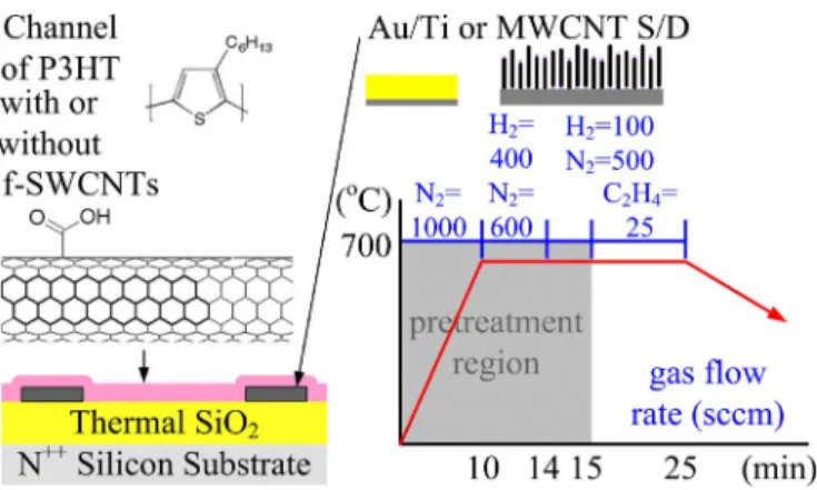
Fig. 1. Scheme of device structure of transistors with F-SWCNT-P3HT channel and an MWCNT S/D. The recipes of MWCNT deposition and the cross-sectional view of electrodes are shown on the right side, and the molecular structure of F-SWCNTs and P3HT are shown at the top.
On that basis, this letter studies the superior performance of PTFTs with a functionalized single-walled CNT-blended poly(3-hexylthiophene) (F-SWCNT-P3HT ) channel and multi-walled CNT S/Ds (MWCNT S/Ds). Compared with transistors with a P3HT channel and gold electrodes, the mobility of transistors with an F-SWCNT-P3HT channel and MWCNT S/Ds is increased by more than one order of magnitude. We propose that this improvement results not only from the well-known fast carrier transport assisted by the blend of F-SWCNTs but also, more importantly, from a reduction in the contact resistance between P3HT and MWCNT S/Ds. A band structure is proposed for the transistor with an F-SWCNT-P3HT channel and MWCNT S/Ds to explain the mechanism for the improve-ment in mobility.
II. EXPERIMENTALPROCEDURE
A schematic cross section of a bottom contact P3HT or F-SWCNT-P3HT TFT possessing an MWCNT S/D and the recipe for growth of the MWCNTs is provided in Fig. 1. An n-type heavily doped Si substrate was used as the gate elec-trode. After standard cleaning, a 200-nm-thick SiO2 layer
was grown by thermal oxidation to be the gate insulator. For MWCNT S/D formation, an Fe/Ti catalytic and buffer layer was then deposited and patterned through electron-beam thermal evaporation and the lift-off technique, producing 0741-3106/$26.00 © 2011 IEEE
1458 IEEE ELECTRON DEVICE LETTERS, VOL. 32, NO. 10, OCTOBER 2011
thicknesses of 5 and 12.5 nm for the Fe/Ti layer, respectively. Subsequently, the MWCNTs were grown through thermal CVD using the following procedure: The samples were heated to 700 ◦C in a nitrogen gas atmosphere. After pretreatment of the Fe/Ti catalytic layer in a mixed gas flow of hydrogen and nitrogen, MWCNTs were grown on the S/D region through pyrolysis of ethylene (C2H4), which is used as the carbon
source, over a growth time of 10 min. The high operating temperature of thermal CVD deposition was not an issue for future application because MWCNTs had already been de-posited at low temperatures by microwave plasma CVD [7]. An Au/Ti S/D, which was 50 and 2.5 nm for Au and Ti, respectively, was prepared for comparison. Prior to the depo-sition of the channels, the substrate was treated by hexamethyl disilazane passivation in a vacuum oven at 150◦C creating a hydrophobic surface. A P3HT or F-SWCNT-P3HT layer was then spun on using a two-step process—1000 rpm for 10 s in the first step and 1500 rpm for 25 s in the second step, followed by baking at 150 ◦C for 3 min. Chloroform was used as the solvent of P3HT and F-SWCNT-P3HT. The weight percentage of solution of P3HT in chloroform was 0.2 wt%, and the weight ratio of F-SWCNTs and P3HT was 1 : 0.2. All of the P3HT and F-SWCNT-P3HT solutions were treated with ultrasonic vibration for 30 min. The regioregular P3HT used in this letter was purchased from FEM, Inc. (Mw = 50000), and the provided coupling ratio of head–tail to head–head and tail–tail was approximately 90%. The carboxylic acid F-SWCNTs with lengths ranging from 0.5 to 1.5 μm and purity of 80% to 90% were purchased from Sigma–Aldrich industries, USA. All the processes of the devices were implemented under atmospheric conditions. The electrical properties were mea-sured by a Hewlett–Packard 4156C semiconductor parameter analyzer and were characterized in ambient air. The devices operated at their saturation region and had a drain voltage of −60 V. The saturation mobility was evaluated at a gate voltage of−60 V by the value of gm,max, for which the formula is
μn=
gmL
WCox(Vgs− Vt)
where Coxand gmare unit-area capacitance and the
differenti-ation of the Idwith respect to Vg.
III. RESULTS ANDDISCUSSION
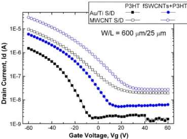
The characteristics of drain current versus gate voltage of transistors with P3HT or F-SWCNT-P3HT channels and gold or MWCNT S/Ds are shown in Fig. 2. The channel length and width were 25 and 600 μm, respectively. Not surprisingly, the transistors with an F-SWCNT-P3HT channel exhibited a superior ON-state current and smaller threshold voltage but a worse subthreshold swing than those with a P3HT channel. The carrier separation between P3HT and CNTs has been widely studied by photoluminescence [8], [9]. Similar improve-ments inON-state current or mobility were also reported [3]. Carriers induced by the gate field could supposedly transfer from P3HT into F-SWCNTs and be transported with high carrier mobility of CNTs. The mobility values of the P3HT and
Fig. 2. Characteristics of drain current versus gate voltage of transistors with a P3HT or F-SWCNT-P3HT channel and gold or MWCNT S/Ds.
F-SWCNT-P3HT channels were 0.0052 and 0.0172 cm2/V· s,
respectively. Worth mentioning is that the mobility of the P3HT channel was already close to the conventional value of 0.001 to 0.01 cm2/V· s when the P3HT layer was processed by a simple spin-on using chloroform as the solvent without involving any special processes or posttreatment [1], [4]. The mobility improvement resulting from the addition of FSWCNTs into the P3HT layer in this letter was only three times, which was much less than that published by Bo et al. We thought that it is due to the fact that, in this letter, the commercial FSWCNTs were blended in P3HT without any further treatment [3]. Optimiz-ing the process of producOptimiz-ing the P3HT and the F-SWCNT-P3HT layer is therefore possible [3]. The small increase in the subthreshold swing might result from the poor interface between the gate oxide and the P3HT or F-SWCNTs. However, despite this small increase, the improved mobility still shows the potential for further applications.
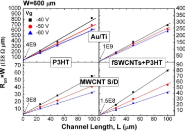
The effect of reduced contact resistance for pentacene-based TFTs with CNT S/Ds had been proposed in previous work by this author and in investigations by another group but not for PTFTs [5], [6]. Moreover, few studies of F-SWCNT-P3HT-based TFTs with CNT S/Ds have been performed. As the results show in Fig. 2, compared with P3HT or F-SWCNT-P3HT-based TFTs with gold S/Ds, the mobility of P3HT or F-SWCNT-P3HT-based TFTs with MWCNT S/D exhibits a dramatic im-provement, which resulted from the effect of reduced contact resistance. The values of contact resistance were extracted by transmission-line measurement (TLM), as shown in Fig. 3. We observed that the devices with an F-SWCNT-P3HT channel and a gold S/D exhibited lower contact resistance. This result might be due to the direct contact of metallic F-SWCNTs and the gold S/D and thus made the carrier transport more easily through metallic F-SWCNTs into the channel. Higher mobility of carriers in the channel could also be observed by the smaller slope of the results of TLM. Therefore, we speculate that the higher carrier mobility resulting from the incorporation of F-SWCNTs led to the higher average mobility of the channel. As a result, with both aforementioned reasons, the higher ON-state current of the device with F-SWCNTs incorporation
CHANG AND CHIEN: F-SWCNT-BLENDED P3HT-BASED TFTs WITH MWCNT S/Ds 1459
Fig. 3. Results of TLM. The values of contact resistance were indicated. was achieved, as compared with that of the conventional de-vice without f-SWCNTs. In addition, when MWCNT S/D was employed, the contact resistance could be further reduced by one order of magnitude. A high field-effect mobility value of 0.0716 cm2/V· s was attained. The larger subthreshold swing
and the OFF-state current might be caused by damage on the gate oxide, which was induced by the diffusion of catalytic material during the formation of MWCNT S/Ds and resulted in a larger gate leakage current. Fortunately, these problems can be overcome by using the low-temperature process for fabricating MWCNTs and a top-gate and bottom-contact device structure [7], [10]. This has two explanations. First, based on the reduced contact resistance, the electric field, which is biased from the drain electrode, could be built up in the channel more effectively so that the ON-state current might be improved. Second, the holes in P3HT could be injected into F-SWCNTs because the work function of F-SWCNTs might be smaller than the highest occupied molecular orbital of P3HT, and the fast transport of holes of F-SWCNTs would still contribute to the overall mobility. Specifically, the work function of F-SWCNTs was 4.8 eV, which was larger than that of SWCNTs, supposedly because they are functionalized [11], [12]. From the result in Fig. 3, the reduction of channel resistance after introducing MWCNT S/Ds could be clearly observed. This might be at-tributed to the more ordered structure of P3HT on MWCNTs than on Au. Moreover, the vertical-aligned MWCNTs might also be helpful for P3HT to be well ordered, which was similar to the edge-on orientation of P3HT on the surface of a treated gate oxide. Better crystallinity of P3HT after introducing CNTs had ever been proposed by Geng et al. [13] For organic thin-film transistors (OTFTs) with P3HT and the Au S/D, the carrier transport could be limited because of plane-on orientation of P3HT on/near the Au S/D, which was reported in [14]. In other words, the effect of carrier scattering by disordered P3HT could be abated. Therefore, the carrier transport or channel resistance could be improved.
IV. CONCLUSION
To summarize, we systematically investigate the effects of devices with F-SWCNT-blended P3HT channels and MWCNT S/Ds. Both reduced contact resistance and increased mobility for the devices with F-SWCNT-P3HT and MWCNT S/Ds were observed. Exceptional performance was demonstrated for the transistors with F-SWCNT-P3HT channels and MWCNT S/Ds. More than one order of magnitude improvement on mobility was easily obtained. The further study of OTFTs could lead to many potential applications.
REFERENCES
[1] H. Sirringhaus, P. J. Brown, R. H. Friend, M. M. Nielsen, K. Bechgaard, B. M. W. Langeveld-Voss, A. J. H. Spiering, R. A. J. Janssen, E. W. Meijer, P. Herwig, and D. M. de Leeuw, “Two-dimensional charge transport in self-organized, high-mobility conjugated polymers,” Nature, vol. 401, no. 6754, pp. 685–688, Oct. 1999.
[2] H. Sirringhaus, N. Tessler, and R. H. Friend, “Integrated optoelectronic devices based on conjugated polymers,” Science, vol. 280, no. 5370, pp. 1741–1744, Jun. 1998.
[3] X. Z. Bo, C. Y. Lee, M. S. Strano, M. Goldfinger, C. Nuckolls, and G. B. Blanchet, “Carbon nanotubes-semiconductor networks for organic electronics: The pickup stick transistor,” Appl. Phys. Lett., vol. 86, no. 18, pp. 182102-1–182102-3, May 2005.
[4] Y. J. Song, J. U. Lee, and W. H. Jo, “Multi-walled carbon nanotubes co-valently attached with poly(3-hexylthiophene) for enhancement of field-effect mobility of poly(3-hexylthiophene)/multi-walled carbon nanotube composites,” Carbon, vol. 48, no. 2, pp. 389–395, Feb. 2010.
[5] C. H. Chang, C. H. Chien, and J. Y. Yang, “Pentacene-based thin-film tran-sistors with multiwalled carbon nanotube source and drain electrodes,”
Appl. Phys. Lett., vol. 91, no. 8, pp. 083502-1–083502-3, Aug. 2007.
[6] A. Southard, V. Sangwan, J. Cheng, E. D. Williams, and M. S. Fuhrer, “Solution-processed single walled carbon nanotube electrodes for organic thin-film transistors,” Org. Electron., vol. 10, no. 8, pp. 1556–1561, Dec. 2009.
[7] M. Chen, C. M. Chen, and C. F. Chen, “Preparation of high yield multi-walled carbon nanotubes by microwave plasma chemical vapor deposi-tion at low temperature,” J. Mater. Sci., vol. 37, no. 17, pp. 3561–3567, Sep. 2002.
[8] J. Geng, B. S. Kong, S. B. Yang, S. C. Youn, S. Park, T. Joo, and H. T. Jung, “Effect of SWNT defects on the electron transfer properties in P3HT/SWNT hybrid materials,” Adv. Funct. Mater., vol. 18, no. 18, pp. 2659–2665, Sep. 2008.
[9] S. Berson, R. de Bettignies, S. Bailly, S. Guillerez, and B. Jousselme, “Elaboration of P3HT/CNT/PCBM composites for organic photovoltaic cells,” Adv. Funct. Mater., vol. 17, no. 16, pp. 3363–3370, Nov. 2007. [10] B. Gburek and V. Wagner, “Influence of the semiconductor thickness on
the charge carrier mobility in P3HT organic field-effect transistors in top-gate architecture on flexible substrates,” Org. Electron., vol. 11, no. 5, pp. 814–819, May 2010.
[11] A. T. Mallajosyula, S. S. K. Iyer, and B. Mazhari, “Conduction properties of carbon nanotubes in P3HT:SWNT bulk heterojunction solar cells,” in
Proc. 33rd IEEE Photovoltaic Spec. Conf., 2008, pp. 1–6.
[12] H. Ago, T. Kugler, F. Cacialli, W. R. Salaneck, M. S. P. Shaffer, A. H. Windle, and R. H. Friend, “Work functions and surface functional groups of multiwall carbon nanotubes,” J. Phys. Chem. B, vol. 103, no. 38, pp. 8116–8121, Sep. 1999.
[13] J. Geng and T. Zeng, “Influence of single-walled carbon nanotubes induced crystallinity enhancement and morphology change on polymer photovoltaic devices,” J. Amer. Chem. Soc., vol. 128, no. 51, pp. 16 827– 16 833, Dec. 2006.
[14] K. Yamamoto, S. Ochiai, X. Wang, Y. Uchida, K. Kojima, A. Ohashi, and T. Mizutani, “Evaluation of molecular orientation and alignment of poly(3-hexylthiophene) on Au (111) and on poly(4-vinylphenol) sur-faces,” Thin Solid Films, vol. 516, no. 9, pp. 2695–2699, Mar. 2008.