利用量子效率與時間解析電激螢光研究鎵極性、氮極性與半極性氮化銦鎵/氮化鎵多重量子井發光二極體之載子傳輸行為
93
0
0
全文
(2) 致謝 碩士班兩年中要感謝很多人,能夠順利完成學業與畢業論文,首要感謝的是 我的父母以及女友宇庭,他們默默地付出,讓我的求學之路無後顧之憂,且感到 更加順遂。其次是我的指導教授馮世維博士,馮老師不僅在學業上不時地給予我 建議和指導,在待人處事上更教導我們要有積極的態度,讓我在面對事情的時候, 往往能有事半功倍的感覺;再者要感謝國立中山大學物理系杜立偉老師,這次的 論文能夠完成,杜老師的實驗室提供了不少實驗資源與意見。最後,要感謝實驗 室的學長-宗憲,以及研究所同學豐益、奕霖、育蓁、一正、在研究所生活中互 相幫忙,讓我的碩士生活充實且快樂;也感謝學弟-宇恩平時幫我分擔雜事且口 試當天大力地相助,讓我能夠順利的通過口試。. 廖柏勛 敬上 2013/08.
(3) 利用量子效率與時間解析電激螢光研究鎵極性、氮極性與半極性氮化銦鎵/ 氮化鎵多重量子井發光二極體之載子傳輸行為 學生:廖柏勛 指導教授:馮 世 維 博士 國立高雄大學應用物理學系研究所. 摘要 首先,我們呈現氮極性與半極性 (11 2 2) 氮化鎵磊晶膜的掃描電子顯微鏡(SEM)、陰 極發光(CL)、原子力顯微鏡(AFM)、光激螢光(PL)以及拉曼(Raman)實驗結果。由於半 極性 (11 2 2) 氮化鎵樣品的表面是屬網狀結構,半極性 (11 2 2) 氮化鎵樣品的表面粗糙度大 於氮極性氮化鎵樣品,所觀察到的線條條紋與粗糙度分別象徵為堆疊差排(SF)與線錯位 (TDs)。換言之,氮極性氮化鎵樣品的缺陷密度高於半極性 (11 2 2) 氮化鎵樣品。陰極發 光強度與原子力顯微鏡量測的結果一致,半極性 (11 2 2) 氮化鎵樣品有較高的陰極發光強 度與較好的晶體品質。對氮極性氮化鎵樣品而言,溫度從10升到300 K,不帶電受體 (A0BE)複合的發光強度比施體-受體對(DAP)複合的發光強度衰減更快。 其次,利用電激螢光(EL)、電流-電壓(I-V)、量子效率(QE)、與時間解析電激螢光 (TREL)研究鎵極性、氮極性、與半極性氮化銦鎵/氮化鎵多重量子井發光二極體之載子 傳輸行為。鎵極性@藍寶石發光二極體的電激螢光(EL)強度優於半極性 (11 2 2) @r-藍寶 石發光二極體;半極性 (11 2 2) @r-藍寶石發光二極體的電激螢光強度優於氮極性@藍寶 石發光二極體;氮極性@藍寶石發光二極體的電激螢光強度優於半極性 (11 2 2) @m-藍寶 石發光二極體。鎵極性@藍寶石發光二極體的半高全寬(FWHM)小於氮極性@藍寶石發 I.
(4) 光二極體;半極性 (11 2 2) @r-藍寶石發光二極體的半高全寬小於半極性 (11 2 2) @m-藍寶 石發光二極體。 時間解析電激螢光的實驗結果顯示,氮極性@藍寶石發光二極體的反應時間比鎵極 性@藍寶石發光二極體短,這表示氮極性@藍寶石發光二極體具有好的載子注入效率。 隨著外加電壓增加,衰減時間減少。因為較大偏壓會減弱量子侷限史塔克效應(QCSE), 衰減時間降低可以解釋為電子和電洞波函數的重疊積分增加。 由於鎵極性@藍寶石發光二極體的內部壓電場方向與氮極性@藍寶石發光二極體 相反,導致鎵極性@藍寶石發光二極體衰減時間隨外加偏壓的趨勢與氮極性@藍寶石發 光二極體隨外加偏壓的趨勢相反。透過量子效率與時間解析電激螢光測量結果,可以決 定出輻射衰減率與非輻射衰減率。鎵極性@藍寶石發光二極體的輻射衰減率比其它三個 發光二極體快;半極性 (11 2 2) @m-藍寶石發光二極體的非輻射衰減率比其它三個發光二 極體快。. 關鍵字:時間解析電激螢光、載子傳輸、反應時間、鎵極性氮化銦鎵/氮化鎵多重量子 井發光二極體、氮極性氮化銦鎵/氮化鎵多重量子井發光二極體、半極性氮化銦鎵/氮化 鎵多重量子井發光二極體. II.
(5) Carrier transport study of Ga-polar, N-polar, and semipolar InGaN/GaN multiple quantum well LEDs by using quantum efficiency and time-resolved electroluminescence measurements. Student:Po-Hsun Liao Advisor:Dr. Shih-Wei Feng Institute of Applied Physics, National University of Kaohsiung. Abstract First, we have shown the experimental results of SEM, CL, AFM, PL, and Raman measurements of the N-polar GaN and semipolar (11 2 2) GaN epilayers. The surface roughness of the semipolar (11 2 2) GaN sample is larger than that of the N-polar GaN sample. The higher surface roughness of the semipolar (11 2 2) GaN was attributed the meshed structure on the surface. The obvious striation feature and roughness were characterized by of SF and TDs. In other words, the defect density of the N-polar GaN sample is higher than that of the semipolar (11 2 2) GaN sample. The result of CL intensity is consistent of that of the AFM measurement. The semipolar (11 2 2) GaN sample reveals the higher CL intensity and the better crystal quality. For the N-polar GaN sample, the intensity of the neutral acceptors (A0BE) recombination decays quickly than that of the donor-acceptor pair (DAP) recombination from 10 to 300 K. III.
(6) Second, the carrier transport behavior of Ga-polar, N-polar, and semipolar InGaN/GaN MQW LEDs are studied by using electroluminescence (EL), current-voltage (I-V), quantum efficiency (QE), and time-resolved electroluminescence (TREL) measurements. The EL intensity of Ga-polar@sapphire LED is better than that of the semipolar@r-sapphire LED; the EL intensity of the semipolar@r-sapphire LED is better than that of the N-polar@sapphire LED;the EL intensity of the N-polar@sapphire LED is better than that of the semipolar@m-sapphire LED. The FWHM (full width at half maximum) of the Ga-polar@sapphire LED is smaller than that of N-polar@sapphire LED;The FWHM of the semipolar@r-sapphire LED is smaller than that of semipolar@m-sapphire LED. From the TREL results, the shorter response time of N-polar@sapphire LED than that of Ga-polar@sapphire LED suggests a better injection efficiency of N-polar@sapphire LED. As the applied voltage increases, the decay time decreases. Because of the slightly weaker quantum confined Stark effect (QCSE) at a larger applied voltage, the decreasing decay time can be explained with the slightly increasing overlap integral of electron and hole wavefunctions. Due to the opposite directions of the internal piezoelectric field of Ga-polar@sapphire and N-polar@sapphire LEDs, the trend of the decay time for the Ga-polar@sapphire LED is opposite with that of N-polar@sapphire LED. From the results of quantum efficiency and TREL measurements, the radiative decay rate and nonradiative decay rate are determined. IV.
(7) The radiative decay rate of Ga-polar@sapphire LED is faster than the other three LEDs. The non-radiative decay rate of semipolar@m-sapphire LED is faster than the other three LEDs.. Keywords:Time-resolved Electroluminescence;Carrier Transport;Response Time; Ga-polar InGaN/GaN MQW LED;N-polar InGaN/GaN MQW LED;Semipolar InGaN/GaN MQW LED. V.
(8) Contents 中文摘要………………………………………………………….………………I Abstract………………………………………………………………………...III Contents………………………………………………………………………...VI Table Captions………………………………………………………………....IX Figure Captions………………………………………………………………....X Chapter 1 Introductions of semipolar (1122) InGaN/GaN Multiple Quantum Wells (MQWs) light-emitting diode…………………………….…1 1.1 Highly stable blue-emission in semipolar (11 2 2) InGaN/GaN mutli-quantum well light-emitting diode……………………………………………........................................1 1.2 Improvement of crystal quality and optical property in (11 2 2) semipolar InGaN/GaN LEDs grown on patterned m-plane sapphire substrate…………………………………...3 References……………………………………………………………………………………..6. Chapter 2 Anisotropic In-plane Strains and Degree of Polarization in N - p o l a r a n d S e m i p o l a r (11 2 2) G a N G r o w n o n m - s a p p h i r e Substrate…………………………………………………………..…….…….12 2.1 Introduction………………………………………………………………………………12 2.2 Motivation and Investigation Flow Chart………………………………………….…….13 VI.
(9) 2.3 Sample Structures and Growth Conditions…………………………………………...….14 2.4 Anisotropic Characteristics of N-polar and Semipolar (1122) GaN Grown on m-sapphire…………………………………………………………………………….…15 2.4.1 Scanning Electron Microscope (SEM) and Cathodoluminescence (CL) Studies of N-polar and Semipolar (1122) GaN Grown on m-sapphire………………...……15 2.4.2 Atomic Force Microscopy (AFM) Studies of of N-polar and Semipolar (1122) GaN Grown on m-sapphire…………………………………………………..……17 2.4.3 Polarization- and Temperature-dependent Photoluminescence (PL) Studies of N-polar and Semipolar (1122) GaN Grown on m-sapphire…………..………….18 2.4.3.1 Low-temperature Polarized PL and Degree of Polarization (DOP)............18 2.4.3.2 Temperature-dependent PL Study...............................................................19 2.4.3.3 Temperature-dependent Polarized PL Study...............................................20 2.4.4 Estimation of Strain by Raman Scattering Measurement………………………...20 2.5 Discussion and Summary..................................................................................................22 References................................................................................................................................23. Chapter 3 Carrier transport study of Ga-polar, N-polar, and semipolar InGaN/GaN multiple quantum well LEDs by using quantum efficiency and time-resolved electroluminescence measurements…………………….……38 VII.
(10) 3.1 Introductions…………………………………………………………...…….……….…..38 3.2 Motivation and Investigation Flow Chart……………………………………………..…41 3.3 Sample Structures and Growth Conditions of LEDs……………………………………..42 3.4 Device Characteristics and Carrier Transport Properties of LEDs……………………….44 3.4.1 Electroluminescence (EL) Studies of LEDs………………………………………44 3.4.2 Current-Voltage (I-V Curve) Studies of LEDs……………………………………47 3.4.3 Luminescence Efficiency Studies of LEDs……………………………………….49 3.4.4 Time-resolved Electroluminescence (TREL) Studies of LEDs…………………..50 3.5 Discussion and Summary...................................................................................................53 References................................................................................................................................55. VIII.
(11) Table Captions Table 2.1 Growth conditions of (a) N-polar GaN and (b) semipolar GaN…………………..27 Table 2.2 ∆ω − A1 (TO ) and ∆ω − E2 (high) for the N-polar and semipolar GaN samples……………………………………………………………………………………….37 Table 3.1 Structure and properties of Ga- and N-polar GaN…………………………..…….60 Table 3.2 Growth conditions of (a) Ga-polar@sapphire, (b) N-polar@sapphire, (c) semipolar@r-sapphire, and (d) semipolar@m-sapphire InGaN LEDs………………………63. IX.
(12) Figure Captions Figure 1.1 Current-voltage characteristic curve of the semipolar (11-22) InGaN/GaN MQW LED. The inset displays the schematic illustration of the fabricated LED structure and the cross-sectional transmission electron microscopy (TEM) image of the semipolar (11 2 2) InGaN/GaN MQW LED………………………………………………………………...…….7 Figure 1.2 EL spectra and as a function of I Inject for the semipolar (11 2 2) InGaN/GaN MQW LED at room temperature. The inset shows the EL image of semipolar (11 2 2) InGaN/GaN MQW LED operated with 20mA at room temperature…………….……………7 Figure 1.3 FWHM and λ EL as a function of I Inject for the semipolar (11 2 2) InGaN/GaN MQW LED. The inset schematically illustrates an example of the energy band diagram for the semipolar InGaN/GaN MQW. The black line represents the potential profile of the semipolar InGaN/GaN MQW when assuming that the QCSE is almost eliminated. The grey line virtually illustrates one of the examples for the potential profiles in the c-plane InGaN/GaN MQW in which the QCSE exists. E c and E v in the energy band diagram mean the conduction band minimum and the valence band maximum, respectively……………………8 Figure 1.4 P out and η ex as a function of I Inject for the semipolar (11 2 2) InGaN/GaN MQW LED………………………………..…………………………………………………………..8 Figure 1.5 Dependence Normalized EL intensity on the polarization degree for the semipolar X.
(13) (11 2 2) InGaN/GaN MQW LED. The inset shows ρ Polar as a function of I Inject for the semipolar (11 2 2) InGaN/GaN MQW LED……………………………………………...…..9 Figure 1.6 (a) and (b) SEM images of the hemispherical patterned m-plane sapphire substrate (HPSS)…………………………….……………………………………………………….....10 Figure 1.7 A 20-μm×20-μm AFM images of the semipolar GaN on (a) planar substrate (height scale:216 nm, RMS roughness of 30 nm ) and (b) HPSS (height scale:161 nm, RMS roughness:23 nm), respectively……………………………………………………...............10 Figure 1.8 (a) Room temperature and (b) low temperature photoluminescence spectra of the semipolar GaN grown on the planar substrate and the HPSS……………………………..…11 Figure 1.9 L–I characteristics of the semipolar InGaN LEDs grown on the planar substrate and the HPSS. The insets are photographic images of the InGaN LED emitting bluish-green light on the planar and HPSS…………………………………………………………………11 Figure 2.1 LT-AlN growth on sapphire (a) inclined SEM and (b) AFM imaging of top surface of r-plane sapphire (1 μm×1 μm). Selectivity of GaN on the AlN buffer is shown by (c) inclined and (d) top view SEM images…………………………………………………...….25 Figure 2.2 Controlled growth evolution of semipolar GaN viewed by growth interruptions and cross-sectional SEM imaging. Under different growth conditions (a), (b), and (c) as labeled, Column (i) first step condition, Column (ii) second step growth conditions are changed to control relative facets growth rates. Column (iii) growth is continued under the XI.
(14) same conditions until before coalescence……………………………………………………25 Figure 2.3 Experimental flow chart of this chapter……………………………………….…26 Figure2.4 Sample structures of (a) N-polar GaN and (b) semipolar (11 2 2) GaN…………27 Figure2.5 (a) SEM and (b) CL experimental setups in a JEOL SEM system (model JSM 7000F)………………………………………………………………………………….…….28 Figure 2.6 SEM images of the (a) N-polar GaN and (b) semipolar (11 2 2) GaN samples and the panchromatic CL images (c) and (d) taken over the same regions with 11kV excitation electron voltage under room temperature, respectively……………………………………...29 Figure 2.7 CL spectra of the (a) N-polar GaN and (b) semipolar (11 2 2) GaN samples with the excitations of 5, 7, 9, and 11kV electron voltages under room temperature…………..…29 Figure 2.8 Experimental setup of AFM measurement……………………………………….30 Figure 2.9 AFM images of the (a) N-polar GaN (Rq:0.5826nm) and (b) semipolar (11 2 2) GaN samples (Rq:1.906nm), and 3D AFM images (c) and (d) taken from the same regions, respectively. Surface roughness of each sample, Rq, is shown in the parentheses…………..30 Figure 2.10 Experimental setup of PL measurement………………………………………..31 Figure 2.11 Polarization-dependent PL at 10K for the (a) N-polar GaN and (b) semipolar (11 2 2) GaN samples……………………………………………………………………..….31 max min Figure 2.12 (Left coordinate) PL spectra with polarization degrees set at φ PL and φ PL for. the (a) N-polar GaN and (b) semipolar (11 2 2) GaN samples at 10K. (Right coordinate) The XII.
(15) degree of polarization for the two samples is also shown………………………………...….32 Figure 2.13 PL spectra as a function of temperature for the (a) N-polar GaN and (b) semipolar (11 2 2) GaN samples…………………………………………………………….33 Figure 2.14 PL peak position as a function of temperature for the N-polar GaN (black and red) and semipolar (11 2 2) GaN (green) samples……………………………………………..…33 max for the (a) Figure 2.15 Temperature-dependent PL with polarization degree set at φ PL. N-polar GaN and (b) semipolar (11 2 2) GaN samples…………………………………..….34 min for the (a) Figure 2.16 Temperature-dependent PL with polarization degree set at φ PL. N-polar GaN and (b) semipolar (11 2 2) GaN samples………………………………...……34 Figure 2.17 The normalized PL integral intensities without polarization and with polarization max min degrees set at φ PL and φ PL for the (a)N-polar GaN and (b) semipolar (11 2 2) GaN. sample as a function of temperature……………………………………………………...…..35 Figure 2.18 Experimental setup of Jobin Yvon-Horiba Micro-Raman system (model T64000)………………………………………………………………………………………36 Figure 2.19 Raman spectra of the N-polar GaN (black) and semipolar (11 2 2) GaN (red) samples under (a) z ' ( x' x' ) z ' and (b) z ' ( y ' y ' ) z ' configurations………………………..…37 Figure 3.1 Milestone of the development of light emitting diodes (LEDs)………………....57 Figure 3.2 Scaling of (a) chip efficiency and (b) lifetime with dislocation density………....57 Figure 3.3 (a) Calculated energy band diagrams of Ga-polar and N-polar InGaN MQW LEDs. XIII.
(16) (b) State of the intrinsic (including both spontaneous and piezoelectric polarization) and bias induced electric fields in the QWs of Ga-polar and N-polar InGaN MQW LEDs…………58 Figure 3.4 Atomic surface model including dangling bonds at < 10 1 0 >, and < 11 2 0 > step edges for (a) Ga-face, and (b) N-face. Sites A Ga ,B Ga , and A N indicate a single-carbon bonding on a group V site, while sites C Ga , D Ga , and B N indicate the bonding of a monomethyl-gallium group. Atoms which are recessed from the surface by one atomic layer are represented by patterned circles………………………………………………………………………………59 Figure 3.5 SIMS data of oxygen concentration as a function of (a) Ga flow, (b) pressure, (c) temperature, and (d) V/III ratio………………………………………………………..……..60 Figure 3.6 Semipolar ( 11 2 2 ) GaN on (a) planar m-sapphire and (b) etched r-sapphire. SEM images of growth interruptions after (c) 2 min, 15 min, and complete growth (2 μm) on planar m-sapphire. (d) Initial selective growth, before, and after coalescence of stripes on etched r-sapphire………………………………………………………………………………...…..61 Figure 3.7 (a)SEM and ( b) AFM images of as-grown 2 μm GaN on m-sapphire. (c) SEM and (d) 3D view of AFM images on LED structure……………………………..........…………..61 Figure 3.8 Experimental flow chart of this chapter……………………………………….…62 Figure 3.9Sample structures of (a) Ga-polar@sapphire, (b) N-polar@sapphire, (c) semipolar@r-sapphire, and (d) semipolar@m-sapphire InGaN LEDs…………………..…..63 XIV.
(17) Figure 3.10 (a) Experimental setup and (b) Schematic diagram of EL images under CW operation……………………………………………………………………………………...64 Figure 3.11 EL images of the Ga-polar@sapphire [(a)-(f)], semipolar@r-sapphire [(g)-(l)], N-polar@sapphire [(m)-(r)], and semipolar@m-sapphire [(s)-(x)] LEDs operated under 2.5-5V CW applied voltages. In EL images, the top and down electrodes correspond to p- and n-contact pads, respectively……………………………………………………………….....64 Figure 3.12 EL spectra of the (a) Ga-polar@sapphire, (b) semipolar@r-sapphire, (c) N-polar@sapphire, and (d) semipolar@m-sapphire LEDs at room temperature with 2.5-6 V CW applied voltages. (e) Normalized EL spectra at room temperature with a 6 V CW applied voltage for the four LEDs………………………………………………………………….…65 Figure 3.13 Peak position of EL spectrum as a function of CW applied voltage for the (a) Ga-polar@sapphire, (b) semipolar@r-sapphire, (c) N-polar@sapphire, and (d) semipolar@m-sapphire LEDs at room temperature………………………………………….65 Figure 3.14 (a) Experimental setup and (b) Schematic diagram of EL images under pulse operation…………………………………………………………………………………..…66 Figure 3.15 EL images of the Ga-polar@sapphire [(a)-(f)], semipolar@r-sapphire [(g)-(l)], N-polar@sapphire [(m)-(r)], and semipolar@m-sapphire [(s)-(x)] LEDs operated with 2.5-5V 1μs pulse width, and 1kHz repetition rate applied pulse voltages. In EL images, the top and down electrodes correspond to p- and n-contact pads, respectively…………………………66 XV.
(18) Figure 3.16 EL spectra of the (a) Ga-polar@sapphire, (b) semipolar@r-sapphire, (c) N-polar@sapphire, and (d) semipolar@m-sapphire LEDs at room temperature with 2.5-5 V 1μs pulse width, and 1kHz repetition rate applied pulse voltages. (e) Normalized EL spectra at room temperature with a 5 V applied pulse voltage for the four LEDs…………………...67 Figure 3.17 Peak position of EL spectrum as a function of applied pulse voltage with 1μs pulse width and 1kHz repetition rate for the (a) Ga-polar@sapphire, (b) semipolar@r-sapphire, (c) N-polar@sapphire, and (d) semipolar@m-sapphire LEDs……...67 Figure 3.18 (a) Leakage current and (b) Current density versus applied voltage (I-V curve) characteristics……………………………………………………………………………..….68 Figure 3.19 (a) Experimental setup of luminescence efficiency. (b) Schematic diagram of an integrating sphere………………………………………………………………………….…69 Figure 3.20 Luminescence efficiency (left coordinate) and normalized quantum efficiency (right coordinate) as functions of applied voltage……………………………………………69 Figure 3.21 (a) Experimental setup and (b) Schematic diagram of time-resolved electroluminescence (TREL)………………………………………………………………....70 Figure 3.22 (a) A short pulse voltage with 1μs pulse width generated from a pulse generator. (b) A rising profile of TREL and the determination of τ response and τ maxEL …………...…….70 Figure 3.23 TREL rising profiles with 2.5-6 volt, 1μs pulse width, and 1kHz repetition rate applied pulse voltages for the (a) Ga-polar@sapphire, (b) semipolar@r-sapphire, (c) XVI.
(19) N-polar@sapphire, and (d) semipolar@m-sapphire LEDs…………………………………..71 Figure 3.24 (a) Response time ( τ response ), (b) the time ( τ maxEL ) at maximum intensity of transit EL, and (c) the time difference ( τ maxEL − τ response ) between ( τ maxEL ) and ( τ response ) as a function of applied pulse voltage for the four LEDs…………………………………………………..72 Figure 3.25 TREL decay profiles with 2.5-6 volt, 1μs pulse width, and 1kHz repetition rate applied pulse voltages for the (a) Ga-polar@sapphire, (b) semipolar@r-sapphire, (c) N-polar@sapphire, and (d) semipolar@m-sapphire LEDs…………………………….…….73 Figure 3.26 (a) Decay time and (b) decay rate as functions of applied pulse voltage for the four LEDs…………………………………………………………………………………….74 Figure 3.27 κ r (filled symbol) and κ nr (unfilled symbol) as functions of applied pulse voltage for the four LEDs………………………………………………………………...…..74. XVII.
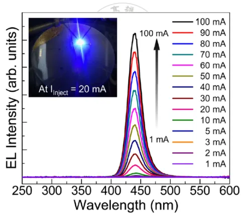
(20) Chapter 1 Introductions of semipolar. (11 2 2). InGaN/GaN. Multiple Quantum Wells (MQWs) light-emitting diode. 1.1 Highly stable blue-emission in semipolar. (11 2 2). InGaN/GaN. mutli-quantum well light-emitting diode Figure 1.1 shows the current density versus applied voltage (I-V curve) characteristics of the semipolar (11 2 2) InGaN/GaN MQW LED. The inset displays the LED structure and the cross-sectional transmission electron microscopy (TEM) image of the semipolar (11 2 2) InGaN/GaN MQW LED. Ti/Al/Ni/Au and indium-tin-oxide (ITO) are used as Ohmic contacts to n- and p-GaN layers, respectively. The relatively high turn-on voltage (~6V) might come from the series resistance attributed to the low Mg incorporation rate (low hole concentration:<1018 cm-3) in semipolar (11 2 2) InGaN/GaN MQW LED [1]. Figure 1.2 shows the EL spectra and as a function of I Inject for the semipolar (11 2 2) InGaN/GaN MQW LED at room temperature. The inset shows the EL image of semipolar (11 2 2) InGaN/GaN MQW LED operated with 20mA at room temperature. As I Inject increases, the EL emission intensity is spectacularly increased because of the increase in charge pumping. The EL image in the inset of Figure 1.2 displays bright blue-emission from the semipolar (11 2 2) InGaN/GaN MQW LED operated with 20mA. These results represent that blue-emission in the DELO-grown semipolar (11 2 2) InGaN/GaN MQW LED is highly 1.
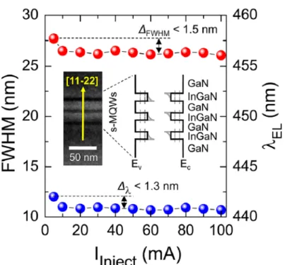
(21) stable at the wide I Inject range [1]. Figure 1.3 shows FWHM and λ EL as a function of I Inject for the semipolar (11 2 2) InGaN/GaN MQW LED. The semipolar (11 2 2) InGaN/GaN MQW LED shows the EL emission at λ EL of 442.1 nm with FWHM of 27.7 nm. As I Inject increases (0<I Inject <10 mA),. λ EL is slightly blue shifted to λ EL of 440.8 nm and FWHM is decreased to 26.1 nm. From I Inject = 10 mA, blue-emission is stabilized at λ EL ~441 nm with the almost identical FWHM~26 nm, even up to I Inject =100 mA. The variations in both peak-wavelength shifts ( ∆ λ ) and emission line-width changes ( ∆ FWHM ) only occur at low I Inject below 10 mA, and the magnitude of ∆ λ is less than 1.3 nm. This is indicative of the reduced QCSE and the lower band-filling effect in the DELO-grown semipolar (11 2 2) InGaN/GaN MQW LED. The inset illustrates the energy band diagram for the semipolar InGaN/GaN MQW. The black line represents the potential profile of the semipolar InGaN/GaN MQW when assuming that the QCSE is almost eliminated. The grey line virtually illustrates the potential profiles in the c-plane InGaN/GaN MQW in which the QCSE exists [1]. Figure 1.4 shows the P out and η ex as a function of I Inject for the semipolar (11 2 2) InGaN/GaN MQW LED. The magnitudes of P out andη ex are 1mW and 1.65%, respectively, when I Inject =20 mA. The obtained P out is comparable to other blue semipolar (11 2 2) InGaN/GaN MQW LED (i.e., P out ~384 μW for blue (11 2 2) LED on semipolar GaN templates and P out ~1.8mW for blue (11 2 2) LED on freestanding GaN. After stabilizing EL 2.
(22) emission (I Inject ≧20 mA), P out is linearly increased with increasing I Inject even up to I Inject = 100 mA, while η ex is slightly decreased due to the efficiency droop effect. The linear dependence of P out on I Inject could be beneficial for the high-power LED applications [1]. Figure 1.5 shows the normalized EL intensity on the polarization degree for the semipolar (11 2 2) InGaN/GaN MQW LED. The inset shows ρ Polar as a function of I Inject for the semipolar (11 2 2) InGaN/GaN MQW LED. The usage of semipolar (11 2 2) InGaN/GaN MQW LED not only allows the reduction in QCSE but also provides the polarized light. The polarization ratio (ρ Polar is independent of I Inject , and the obtainedρ Polar value is comparable to other semipolar. (11 2 2). InGaN/GaN MQW LED (i.e.,. ρ Polar ~0.06–0.11 for blue semipolar (11 2 2) InGaN/GaN MQW LED on semipolar GaN templates) [1].. 1.2 Improvement of crystal quality and optical property in (11 2 2) semipolar InGaN/GaN LEDs grown on patterned m-plane sapphire substrate Semipolar GaN layers were grown on the m-plane hemispherical patterned sapphire substrates (HPSS) in order to reduce the defect density and enhance the extraction efficiency of light [2]. The semipolar GaN epilayers were simultaneously grown on the HPSS and the planar 3.
(23) m-plane sapphire substrates by metal organic chemical vapor deposition. Prior to the growth, the sapphire substrate was patterned by dry etching to form a distributed array of hemispherical shapes, as shown in Figure 1.6 (a) and (b) [2]. Figure 1.7 (a) and (b) shows the AFM images of the GaN layers grown on the planar sapphire and the HPSS, respectively. The diffusion length of surface adatoms to ward crystallographic directions such as [11 2 3 ] and [1 1 00] owing to the crystallographic difference between the m-plane sapphire and semipolar (11 2 2) GaN . The roughness values of the GaN surface grown on the planar sapphire and the HPSS were 30 and 23 nm, respectively. The crystalline quality of the GaN layer could be improved via the lateral epitaxial overgrowth on the HPSS [2]. Figure 1.8 (a) shows the room-temperature PL spectra of GaN layer on the planar sapphire and on the HPSS. The intensity of the near band-edge (NBE) emission of the semipolar GaN on the HPSS was approximately three times that of the semipolar GaN on the planar sapphire, which is considered to be caused by the improvement of the crystal quality and the enhancement of the light extraction on the HPSS. The low temperature PL was measured at a temperature of 13K, as shown in Figure 1.8 (a). Both the semipolar GaN layers grown on the m-plane planar sapphire and the HPSS showed a band-edge emission, which was assigned to the donor bound exciton recombination D 0 X, at the same energy (3.48eV). The NBE emission from the HPSS semipolar GaN was approximately one order of 4.
(24) magnitude stronger than that from the planar semipolar GaN layer. This result also suggests that the regrowth process on the surface with the array of hemispheres reduced the defects and improved the extraction efficiency when compared with the direct growth on the planar substrate. Two additional emission bands at 3.42 eV and 3.32 eV are observed in both samples, which are attributed to the luminescence from the BSFs and the PDs, respectively [2]. Figure 1.9 shows the EL of the semipolar InGaN-based LED wafers grown on the planar sapphire and on the HPSS. The insets are EL images of InGaN LED emitting bluish-green light on the planar sapphire and HPSS. The emission peak wavelengths of the planar LED and the HPSS LED are 502 nm and 489 nm at 100 mA, respectively. The blue-shift in the EL peaks between the planar LED and the HPSS LED is attributed to the reduction in defects such as BSFs and perfect dislocations in the HPSS GaN layer. In addition, the output power of the InGaN LED on the HPSS was approximately 1.5 times that of the InGaN LED on the planar substrate [2].. 5.
(25) References 1. D. S. Kim, S. Lee, D. Y. Kim, S. K. Sharma, S. M. Hwang, and Y. G. Seo , Appl. Phys. Lett. 103, 021111 (2013). 2. J. Jang, K. Lee, J. Hwang, J. Jung, S. Lee, K. Lee, B. Kong, H. Cho, O. Nama, J. Cryst. Growth 361 (2012) 166–170.. 6.
(26) Figure 1.1 Current-voltage curve of the semipolar (11 2 2) InGaN/GaN MQW LED. The inset displays the fabricated LED structure and the cross-sectional transmission electron microscopy (TEM) image of the semipolar (11 2 2) InGaN/GaN MQW LED [1].. Figure 1.2 EL spectra and as a function of I Inject for the semipolar (11 2 2) InGaN/GaN MQW LED at room temperature. The inset shows the EL image of semipolar (11 2 2) InGaN/GaN MQW LED operated with 20mA at room temperature [1].. 7.
(27) Figure 1.3 FWHM and λ EL as a function of I Inject for the semipolar (11 2 2) InGaN/GaN MQW LED. The inset illustrates an example of the energy band diagram for the semipolar InGaN/GaN MQW. The black line represents the potential profile of the semipolar InGaN/GaN MQW when assuming that the QCSE is almost eliminated. The grey line virtually illustrates the potential profiles in the c-plane InGaN/GaN MQW. E c and E v in the energy band diagram mean the conduction band minimum and the valence band maximum, respectively [1].. Figure 1.4 P out and η ex as a function of I Inject for the semipolar (11 2 2) InGaN/GaN MQW LED [1].. 8.
(28) Figure 1.5 Normalized EL intensity on the polarization degree for the semipolar (11 2 2) InGaN/GaN MQW LED. The inset shows ρ Polar as a function of I Inject for the semipolar (11 2 2) InGaN/GaN MQW LED [1].. 9.
(29) Figure 1.6 (a) and (b) SEM images of the hemispherical patterned m-plane sapphire substrate (HPSS) [2].. Figure 1.7 AFM images of the semipolar GaN on (a) planar substrate (height scale:216 nm, RMS roughness of 30 nm ) and (b) HPSS (height scale:161 nm, RMS roughness:23 nm) [2 ].. 10.
(30) Figure 1.8 (a) Room temperature and (b) low temperature photoluminescence spectra of the semipolar GaN grown on the planar substrate and the HPSS [2].. Figure 1.9 L–I characteristics of the semipolar InGaN LEDs grown on the planar substrate and the HPSS. The insets are EL images of the InGaN LED emitting bluish-green light on the planar and HPSS [2]. 11.
(31) Chapter. 2. Anisotropic. In-plane. Strains. and. Degree. of. Polarization in N-polar GaN and Semipolar (11 2 2) GaN Grown on r-sapphire Substrate. 2.1 Introduction For AlN, the expected epitaxial relations on the exposed sapphire facets are a-plane AlN on r-plane sapphire and c-plane AlN on c-plane sapphire. In Figure 2.1 (a) and (b), the low-temperature 20 nm AlN buffer nucleates on all sidewalls and surfaces of sapphire. The surface migration distances are low. This is likely because of the high bond strength of AlN limiting the surface diffusion across facets, suggesting this to be the limiting migration mechanism. With such a LT-AlN buffer, subsequent GaN growth consists of a competition between c-GaN on the c-oriented AlN on sidewalls and a-GaN on a-AlN on the top and bottom r-plane sapphire. Given a marginally higher mismatch strain for a-GaN on a-AlN (-2.5% along m-axis and -4.1% along c-axis) than that for the c-axis hetero epitaxy, growth selectivity can be expected to be achieved. As shown in Figure 2.1 (c) and (d), complete selectivity is achieved in the c-plane sidewall growth at 1030°C, 200mbar, and a V/III ratio of 1000 [1]. In Figure 2.2, the resulting crystal shapes are shown when continuing growth from stage 12.
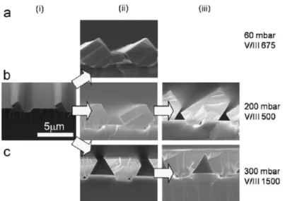
(32) 1 (Figure 2.1 (c)) as a result of different sets of growth conditions used to shape the crystal stripes. The tunability of growth structures is evident with the controlled variation of V/III, temperature and pressure. The purpose of designing the growth shape in this step is to allow for defect reduction, as well as resulting in smooth GaN films. Using total reactor pressure of 60 mbar in the second step growth condition still shows unselective a-plane GaN growth, indicating nucleation occurs despite the existence of other GaN crystal facets. Row (b) of Figure 2.2 shows growth at higher pressure (300 mbar) and low V/III (500), which tends to speed up the c-plane facet and slow down the a-plane. This results void between the stripes remain after continued growth, delaying coalescence likely due to reduced amount of precursors reaching between the crystals. As shown in row (c) of Figure 2.2, the growth conditions of 1000 °C, 300 mbar and V/III ratio of 1500 were chosen to enhance lateral growth (increasing the growth velocity of the c and/or a-plane facets relative to the semipolar facet) and obtain a flat (11 2 2) surface. The choice of this growth condition allows for defect reduction as well as smooth surface morphology, since the defect structure of the GaN stripe islands do not require the excessive overgrowth (as in Figure 2.2 (b)) that delays coalescence of the film [1].. 2.2 Motivation and Investigation Flow Chart Due to large lattice mismatch, there are high densities of defects for GaN grown on 13.
(33) sapphire. In other to reduce defect density, semipolar can reduce the internal piezoelectric field. In this chapter, we investigate the anisotropic properties of N-polar GaN and semipolar (11 2 2) GaN.. Figure 2.3 shows the experimental flow chart of this chapter. By scanning electron microscope (SEM) and cathodoluminescence (CL), the microstructures and nano-photonics of samples are investigated. By atomic force microscopy (AFM) measurement, the surface morphologies of samples are measured. By polarization- and temperature-dependent photoluminescence (PL), the optical properties of the N-polar GaN and semipolar (1122) GaN samples are investigated. The frequency shift of phonon lines and strain inside the samples are investigated by Raman scattering measurements. According to the results of the experiments, we will discuss the anisotropic characteristics of the N-polar GaN and semipolar (11 2 2) GaN grown on r-sapphire.. 2.3 Sample Structures and Growth Conditions Figure 2.4 shows sample structures of (a) N-polar GaN and (b) semipolar (1122) GaN. Table 2.1 shows growth conditions of (a) N-polar GaN and (b) semipolar (1122) GaN. N-polar GaN growths was carried out on 2°miscut sapphire substrate in a horizontal metalorganic chemical vapor deposition reactor. The substrate was 2°miscut towards the [11 2 0] direction. For N-polar GaN growth, sapphire was heated up in a mixture of NH 3 (3 14.
(34) SLM) and N 2 (4 SLM) to 950 °C for 30 s. A LT-GaN buffer (30 nm thick) was grown on nitridized sapphire at 600 °C in H 2 , followed by N-polar GaN growth at 1050 °C and 100 mbar. Growth of semipolar (11 2 2) GaN on these patterned substrates was performed using an Aixtron 200/4RF-S horizontal metalorganic chemical vapor deposition (MOCVD) reactor. Trimethylgallium (TMGa), Trimethylaluminum (TMAl), and ammonia were used as the precursors for Ga, Al, and N, respectively. The etched r-sapphire was thermally cleaned in H 2 ambient at1100 °C, followed by deposition of a 20 nm low-temperature (LT) AlN buffer at 500 °C and 100 mbar. Temperature was then ramped up to anneal the buffer layer, and growth of GaN commenced at 1030 °C. The design of amultiple step growth procedure was implemented in stages (1)-(3):(1) to achieve selective growth on the sapphire sidewall (350 nm GaN, 1030 C, 200mbar, high V/III (low growth rate)), (2) to shape the stripe for optimum coalescence (2.3um GaN, 1030 C, 200mbar, low V/III), (3) and to obtain a flat surface morphology (2.3um GaN, 995 C, 300mbar, high V/III). The growth conditions necessary for each stage are discussed in Reference [1].. 2.4 Anisotropic Characteristics of N-polar GaN and Semipolar (11 2 2) GaN Grown on r-sapphire 2.4.1 Scanning Electron Microscope (SEM) and Cathodoluminescence (CL) 15.
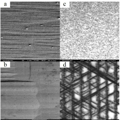
(35) Studies of N-polar GaN and Semipolar (11 2 2) GaN Grown on r-sapphire In other to investigate the relation between optical property and microstructures, scanning electron microscope (SEM) and cathodoluminescence (CL) measurements were conducted at the same regions. As shown in Figure 2.5, SEM and CL images were acquired with a Gatan monoCL3 spectrometer in a JEOL SEM system (model JSM 7000F) under room temperature. The excitation electron voltage for CL measurement ranges from 5 to 11 kV. Figure 2.6 (a) and (b) show the SEM images for the N-polar GaN and semipolar (11 2 2) GaN samples, respectively. In these samples, striation features were observed in the morphology. The surface roughness of N-polar GaN is flatter than semipolar (11 2 2) GaN sample. Two region structures are easy to be observed in the semipolar (11 2 2) GaN sample. The obvious striation feature and roughness were characterized by surface-pits and SFs. In Figure 2.6 (a) and (b), the N-polar GaN sample has striation in lateral direction, yet the semipolar (11 2 2) GaN sample has two kinds of striation on the surface. One can observe the shallow striation in lateral direction of the Figure 2.6 (b). It is suggested the N-polar GaN sample has a higher defect density than that of the semipolar (11 2 2) GaN sample. In addition, Figure 2.6 (c) and (d) show the panchromatic CL images for the corresponding SEM region with 11 kV excitation electron voltages under room temperature. Figure 2.6 (d) shows the meshed structure on the surface of the semipolar (11 2 2) GaN sample. The 16.
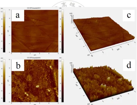
(36) semipolar (11 2 2) GaN sample is brighter than the N-polar GaN sample. The result shows that the density of SF for the N-polar GaN sample is larger than that of the semipolar (11 2 2) GaN sample. Figure 2.7 shows the CL spectra taken from the same SEM regions under room temperature. In the N-polar GaN sample, the weak CL intensities for the emission band reveal a poor sample quality. Due to the lower SF density and a better sample quality, the semipolar (11 2 2) GaN sample has higher CL intensities than that of the N-polar GaN sample. As a result, the results are consistent with the brightness of CL images that mentioned above.. 2.4.2 Atomic Force Microscopy (AFM) Studies of N-polar GaN and Semipolar (11 2 2) GaN Grown on r-sapphire In other to study the surface morphology of the N-polar GaN and semipolar (11 2 2) GaN samples, AFM measurement was conducted. Figure 2.8 shows experimental setup of AFM measurement. AFM images were acquired with XE-70 and XE control electronics under non-contact mode. Figure 2.9 (a) and (b) show AFM images of the N-polar GaN and semipolar (11 2 2) GaN samples, while Figure 2.9 (c) and (d) show 3D AFM images taken from the same regions, respectively. Surface roughness (Rq) of the N-polar GaN and semipolar (11 2 2) GaN samples are 0.5826 and 1.906 nm, respectively. For the semipolar (11 2 2) GaN 17.
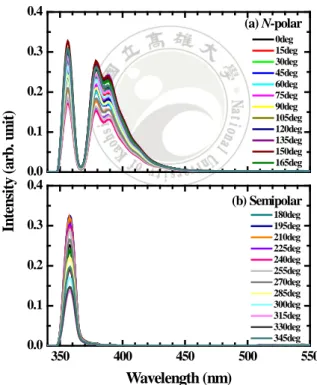
(37) samples, the higher roughness and higher CL intensity were observed. In general, sample with high CL intensity usually has lower roughness. It is suggested that the roughness of the semipolar (11 2 2) GaN sample is contributed from two structures of the semipolar (11 2 2) GaN sample in Figure 2.6.. 2.4.3 Polarization- and Temperature-dependent Photoluminescence (PL) Studies of N-polar GaN and Semipolar (11 2 2) GaN Grown on r-sapphire PL is the most fundamental measurement for understanding the optical property of a material. The experimental setup for PL measurement is shown in Figure 2.10. PL measurements are carried out with the 325 nm line of a 55 mW He-Cd laser for excitation. The samples are placed in a cryostat for temperature-dependent PL measurement.. 2.4.3.1 Low-temperature Polarized PL and Degree of Polarization (DOP) In other to investigate the effect of anisotropic strain on the optical properties, the polarized PL measurement was conducted. Figure 2.11 (a) and (b) show the polarized PL measurement for the N-polar GaN and semipolar (11 2 2) GaN samples, respectively. The PL spectra show a high polarization anisotropy. The degree of polarization (DOP), ρ, can be expressed as. ρ=. I [1 1 00] − I [1 1 23]. I [1 1 00] + I [1 1 23] 18.
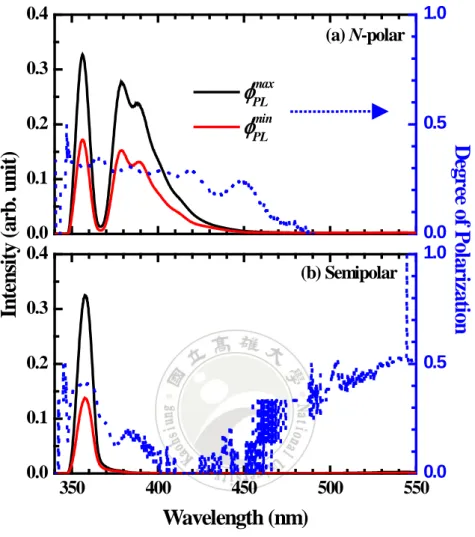
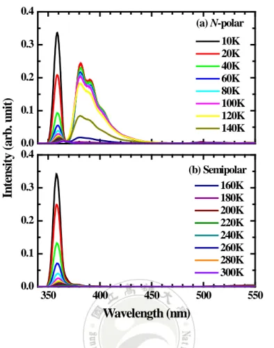
(38) where I[1 1 00] and I[ 1 1 23] are the PL intensities for E //[1 1 00] and E ⊥ [ 1 1 23] , respectively [16]. Figure 2.12 (a) and (b) show the DOP for the two samples. The DOP of the semipolar (11 2 2) GaN sample is larger than that of the N-polar GaN sample.. 2.4.3.2 Temperature-dependent PL Study Figure 2.13 (a) and (b) show the PL spectra of the N-polar GaN and semipolar (11 2 2) GaN samples as a function of temperature, respectively. In Figure 2.13 (a), the N-polar GaN sample has three peaks ~359 nm (3.454 eV), ~382 nm (3.246 eV), and ~391 nm (3.171 eV) under temperatures 10 ~ 100K. The dominate peak is around ~359 nm (3.454 eV). In Figure 2.13 (b), the dominate peak of semipolar (11 2 2) GaN is 357.8 nm (3.466 eV). The emission peak around ~358 nm is neutral acceptors (A0BE) recombination [18], while the emission peaks around ~382 nm and ~391 nm is the relative intensities of the DAP recombination [19]. In the N-polar GaN sample, PL intensity of neutral acceptors (A0BE) recombination decays quicker than that of DAP recombination with increasing temperature. The PL peak positions as a function of temperature for the two samples are shown in Figure 2.14. The peak positions of the N-polar GaN sample are distinguished into two parts. One spectral range is from 335 nm to 370 nm, and the other is from 370 nm to 460 nm. The N-polar GaN and semipolar (11 2 2) GaN samples are 359 and 357.8 nm when the peak position is at 10K. With increasing temperature from 10 to 300 K, both PL peak positions of 19.
(39) the first part (wavelength 335 nm ~ 370 nm) of the N-polar GaN and semipolar (11 2 2) GaN samples are red-shifted, while that of the second part (370 nm ~ 460 nm) of the N-polar GaN sample does not change greatly.. 2.4.3.3 Temperature-dependent Polarized PL Study Figure 2.15 (a) and (b) show the PL spectra with polarization degree set at the largest max intensity φ PL for the N-polar GaN and semipolar (11 2 2) GaN samples as a function of. temperature, respectively. Figure 2.16 (a) and (b) show the PL spectra with polarization min for the N-polar GaN and semipolar (11 2 2) GaN degree set at the smallest intensity φ PL. samples as a function of temperature, respectively. Figure 2.17 (a) and (b) show the normalized PL integral intensities without polarization and with polarization degrees set at max min and φ PL for the N-polar GaN and semipolar (11 2 2) GaN samples as a function of φ PL. temperature, respectively. As the temperature increases, the integral PL intensity of normal, max min MAX ( φ PL ), and MIN ( φ PL ) decrease. For the semipolar (11 2 2) GaN sample, integral min max max is larger than that of φ PL and the integral PL intensity of φ PL is PL intensity of φ PL. stronger than that of Normal.. 2.4.4 Estimation of Strain by Raman Scattering Measurement As shown in Figure 2.18, Raman spectra were recorded in the backscattering 20.
(40) configuration using a Jobin Yvon-Horiba Micro-Raman system (model T64000) under a 532 nm excitation laser. A polarizer was set between the laser and the measured sample to polarize the laser light. Raman scattering can measure the frequency shift of phonons of the N-polar GaN and semipolar (1122) GaN sample. The strain distribution in (1122) GaN can be estimated by Raman scattering. In Figure 2.19 (a) and (b), the Cartesian axes x′ , y′ , and z ′ correspond to the [1 1 00] , [ 1 1 23] , and [11 2 2] directions of GaN, respectively [10]. The z ′( x′x′) z ' and z ′( y′y′) z ' called Porto’s notation. It was used to describe the scattering geometry:the letters outside the parentheses represent the direction of the incident and scattered light, while the letters inside the parentheses represent the incident and scattered polarizations [20] Figure 2.19 shows the Raman scattering spectra for the two samples. The spectra displays A 1 (TO) and E 2 (high) mode for GaN. The solid lines at 531.8 cm-1 and 568.0 cm-1 show the strain-free GaN of A 1 (TO) and E 2 (high) mode, respectively. Compressive stress in the GaN thin film tends to shift Raman peak to a larger wave number, while tensile stress moves the peak to an opposite direction. Based on the deformation potential approximation, the frequency shift, ∆ω = ω − ω0 , can be defined as a function of the strain, where ω 0 represents the phonon frequency of strain-free. The ∆ω and in-plane strain can be influenced by the growth parameters. Table 2.2 shows ∆ω of A 1 (TO) and E 2 (high) mode for the N-polar GaN and semipolar (11 2 2) GaN samples. 21.
(41) 2.5 Discussion and Summary In summary, we have shown the experimental results of SEM, CL, AFM, PL, and Raman measurements of the N-polar GaN and semipolar (11 2 2) GaN samples. The surface roughness of the semipolar (11 2 2) GaN sample is larger than that of the N-polar GaN sample. The higher surface roughness of the semipolar (11 2 2) GaN sample was attributed the meshed structure on the surface. The obvious striation feature and roughness were characterized by of SF and TDs. In other words, the defect density of the N-polar GaN sample is higher than that of the semipolar (11 2 2) GaN sample. The result of CL intensity is consistent of that of the AFM measurement. The semipolar (11 2 2) GaN sample reveals the higher CL intensity and the better crystal quality. For the N-polar GaN sample, the intensity of the neutral acceptors (A0BE) recombination decays quickly than that of the DAP recombination from 10 K to 300 K.. 22.
(42) References 1. B. Leung, Q. Sun, C. Yerino, Y. Zhang, Jung Han, B. H. Kong, H. K. Cho, K. Y. Liao, Y. L. Li, J. Cryst. Growth 341 (2012) 27-33. 2. H. Amano, N. Sawaki, I. Akasaki, Y. Toyoda, Appl. Phys. Lett. 48, 353 (1986). 3. I. Akasaki, H. Amano, Y. Koide, K. Hiramatsu, N. Sawaki, J. Cryst. Growth 98, 209 (1989). 4. J.N. Kuznia, M. Asif-Khan, D.T. Olson, R. Kaplan, J. Freitas, J. Appl. Phys. 73, 4700 (1993) 5. L. Sugiura, K. Itaya, J. Nishio, H. Fujimoto, Y. Kokubun, J. Appl. Phys. 82, 4877 (1997). 6. K. Hiramatsu, S. Itho, H. Amano, et al., J. Cryst. Growth 115, 628 (1991). 7. X.H. Wu, D. Kapolnek, E.J. Tarsa, et al., Appl. Phys. Lett. 68, 1371 (1996). 8. Nichia Chemical Industries, Ltd., 491 Oka, Kaminaka, Anan, Tokushima 774 Jpn. J. Appl. Phys. 30, 1705 (1991) 9. Qian Sun, Benjamin Leung, Christopher D. Yerino, Yu Zhang, and Jung Han, Appl. Phys. Lett. 95, 231904 (2009). 10. M. Funato, D. Inoue, M. Ueda, Y. Kawakami, Y. Narukawa, and T. Mukai, J. Appl. Phys. 107, 123501 (2010). 11. Benjamin Leung, Yu Zhang, Christopher D Yerino, Jung Han, Qian Sun, Zhen Chen, Steve Lester, Kuan-Yung Liao and Yun-Li Li, Semicond. Sci. Technol. 27, 024016 23.
(43) (2012). 12. Sun Q, Yerino C D, Ko T-S, Cho Y S, Lee I-H, Han J and Coltrin M E, J. Appl. Phys. 104, 093523 (2008). 13. A. Kahouli, N. Kriouche, J. Brault, B. Damilano, P. Venne´gue`s, P. de Mierry, M. Leroux, A. Courville, O. Tottereau, and J. Massies, J. Appl. Phys. 110, 084318 (2011) 14. T. Wernicke, S.Ploch, V. Hoffmann, A. Knauer, M. Weyers, and M. Kneissl, Phys. Status Solidi B. 248, 574 (2011). 15. Q. Sun, B. H. Kong, C. D. Yerino, T. S. Ko, B. Leung, H. K. Cho, and J. Han, J. Appl. Phys. 106, 123519 (2009). 16. K. Hiramatsu, K. Nishiyama, A. Motogaito, H. Miyake, Y. Iyechika, and T. Maeda, Phys. Status Solidi A 176, 535 (1999) 17. M. Ueda, K. Kojima, M. Funato, and Y. Kawakami, Appl. Phys. Lett. 89, 211907 (2007). 18. V.Kirikyuk, A.R.A. Zauner, P.C.M. Christianen, J. L. Weyher, P.R. Hageman, P.K. Larsen, J. Cryst. Growth 230 (2001) 477-480. 19. A. Y. Polyakov, N. B. Smirnov, A. V. Govorkov, Q. Sun, Y. Zhang, Y. S. Cho, I.-H. Lee, J. Han, Materials Science and Engineering B 166 (2010) 83–88 20. Bottcher T, Einfeldt S, Figge S, Chierchia R, Heinke H, Hommel D and Speck J S 2001 Appl. Phys. Lett. 78 (1976).. 24.
(44) Figure 2.1 LT-AlN growth on sapphire (a) inclined SEM and (b) AFM imaging of top surface of r-plane sapphire (1 μm×1 μm). Selectivity of GaN on the AlN buffer is shown by (c) inclined and (d) top view SEM images [1].. Figure 2.2 Controlled growth evolution of semipolar GaN viewed by growth interruptions and cross-sectional SEM imaging. Under different growth conditions (a), (b), and (c) as labeled, Column (i) first step condition, Column (ii) second step growth conditions are changed to control relative facets growth rates. Column (iii) growth is continued under the same conditions until before coalescence [1].. 25.
(45) N-polar GaN and Semipolar (1122) GaN grown on r-sapphire by MOCVD. Sample preparation. Scanning Electron Microscope (SEM) and Cathodoluminescence. To investigate microstructures and. (CL) studies. nanophotonics of samples. Atomic Force Microscopy (AFM). To measure the surface. Measurements. morphology of samples. Polarization- and Temperature-dependent Photoluminescence (PL) Studies. To investigate optical properties of samples. To investigate the frequency shifts. Raman Scattering Measurements. of phonon lines and in-plane strains. To discuss the anisotropic characteristics of N-polar GaN and Semipolar (1122) GaN grown. Experimental comparison. on r-sapphire. Figure 2.3 Experimental flow chart of this chapter.. 26.
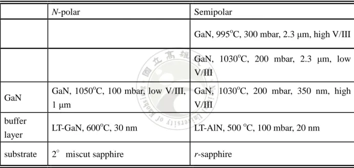
(46) (a). (b). Figure 2.4 Sample structures of (a) N-polar GaN and (b) semipolar (11 2 2) GaN.. N-polar. Semipolar GaN, 995oC, 300 mbar, 2.3 μm, high V/III GaN, 1030oC, 200 mbar, 2.3 μm, low V/III. GaN. GaN, 1050oC, 100 mbar, low V/III, GaN, 1030oC, 200 mbar, 350 nm, high 1 μm V/III. buffer layer. LT-GaN, 600oC, 30 nm. LT-AlN, 500 oC, 100 mbar, 20 nm. substrate. 2°miscut sapphire. r-sapphire. Table 2.1 Growth conditions of (a) N-polar GaN and (b) semipolar (11 2 2) GaN.. 27.
(47) (a). (b). Figure 2.5 (a) SEM and (b) CL experimental setups in a JEOL SEM system (model JSM 7000F).. 28.
(48) Figure 2.6 SEM images of the (a) N-polar GaN and (b) semipolar (11 2 2) GaN samples and the panchromatic CL images (c) and (d) taken over the same regions with 11kV excitation electron voltage under room temperature, respectively.. 20000 (a) N-polar 15000. Intensity (arb. unit). 10000 5000 0 140000 (b) Semipolar 5kV 7kV 9kV 11kV. 120000 100000 80000 60000 40000 20000 0 300. 350. 400. 450. 500. 550. 600. Wavelength (nm). Figure 2.7 CL spectra of the (a) N-polar GaN and (b) semipolar (11 2 2) GaN samples with the excitations of 5, 7, 9, and 11kV electron voltages under room temperature. 29.
(49) Figure 2.8 Experimental setup of AFM measurement.. Figure 2.9 AFM images of the (a) N-polar GaN (Rq:0.5826nm) and (b) semipolar (11 2 2) GaN (Rq:1.906nm) samples, and 3D AFM images (c) and (d) taken from the same regions, respectively. Surface roughness of each sample, Rq, is shown in the parentheses.. 30.
(50) Figure 2.10 Experimental setup of PL measurement.. 0.4 (a) N-polar 0deg 15deg 30deg 45deg 60deg 75deg 90deg 105deg 120deg 135deg 150deg 165deg. 0.3. Intensity (arb. unit). 0.2 0.1 0.0 0.4. (b) Semipolar 180deg 195deg 210deg 225deg 240deg 255deg 270deg 285deg 300deg 315deg 330deg 345deg. 0.3 0.2 0.1 0.0. 350. 400. 450. 500. 550. Wavelength (nm). Figure 2.11 Polarization-dependent PL at 10K for the (a) N-polar GaN and (b) semipolar (11 2 2) GaN samples.. 31.
(51) 1.0. 0.4 (a) N-polar 0.3. φmax PL φmin PL. 0.5. 0.1 0.0 1.0. 0.0 0.4 (b) Semipolar 0.3. Degree of Polarization. Intensity (arb. unit). 0.2. 0.5. 0.2 0.1 0.0. 350. 400. 450. 500. 0.0 550. Wavelength (nm). max min Figure 2.12 (Left coordinate) PL spectra with polarization degrees set at φ PL and φ PL for the (a) N-polar GaN and (b) semipolar (11 2 2) GaN samples at 10K. (Right coordinate) The. degree of polarization for the two samples is also shown.. 32.
(52) 0.4 (a) N-polar 10K 20K 40K 60K 80K 100K 120K 140K. 0.3. Intensity (arb. unit). 0.2 0.1 0.0 0.4. (b) Semipolar 160K 180K 200K 220K 240K 260K 280K 300K. 0.3 0.2 0.1 0.0. 350. 400. 450. 500. 550. Wavelength (nm) Figure 2.13 PL spectra as a function of temperature for the (a) N-polar GaN and (b) semipolar (11 2 2) GaN samples.. 385. Peak Position (nm). 380 375 N-polar (335 nm ~ 370 nm) N-polar (370 nm ~ 460 nm) Semipolar. 370 365 360 355 0. 50. 100. 150. 200. 250. 300. Temperature (K). Figure 2.14 PL peak position as a function of temperature for the N-polar GaN (black and red) and semipolar (11 2 2) GaN (green) samples. 33.
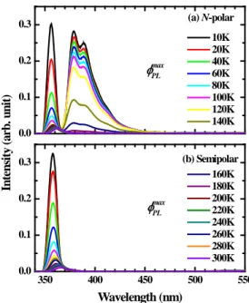
(53) (a) N-polar. 0.3. Intensity (arb. unit). 0.2. 10K 20K 40K 60K 80K 100K 120K 140K. φmax PL. 0.1 0.0 0.3 0.2. φmax PL. 0.1 0.0. 350. 400. (b) Semipolar 160K 180K 200K 220K 240K 260K 280K 300K. 450. 500. 550. Wavelength (nm). max Figure 2.15 Temperature-dependent PL with polarization degree set at φ PL for the (a). N-polar GaN and (b) semipolar (11 2 2) GaN samples.. 0.2 (a) N-polar. φmin PL. 0.1. Intensity (arb. unit). 10K 20K 40K 60K 80K 100K 120K 140K. 0.0 0.2. φmin PL. 0.1. 0.0. 350. 400. (b) Semipolar 160K 180K 200K 220K 240K 260K 280K 300K. 450. 500. 550. Wavelength (nm). min Figure 2.16 Temperature-dependent PL with polarization degree set at φ PL for the (a). N-polar GaN and (b) semipolar (11 2 2) GaN samples. 34.
(54) 1.0. (a) N-polar Normal (335 nm ~ 370 nm) MAX (335 nm ~ 370 nm) MIN (335 nm ~ 370 nm) Normal (370 nm ~ 460 nm) MAX (370 nm ~ 460 nm) MIN (370 nm ~ 460 nm). Integral Intensity (arb. unit). 0.8 0.6 0.4 0.2 0.0 1.0. (b) Semipolar Normal MAX MIN. 0.8 0.6 0.4 0.2 0.0 0. 50. 100. 150. 200. 250. 300. Temperature (K). Figure 2.17. The normalized PL integral intensities without polarization and with. max min polarization degrees set at φ PL and φ PL for the (a)N-polar GaN and (b) semipolar. (11 2 2) GaN sample as a function of temperature.. 35.
(55) Figure 2.18 Experimental setup of Jobin Yvon-Horiba Micro-Raman system (model T64000).. 36.
(56) z' ( xy' yx' ) z'. 9. Intensity (arb. unit). 6. A1(TO). E2(high). z' ( x ' x ' ) z' (a). ∆ω = 1.78. ∆ω = 0.359. N-polar Semipolar. ∆ω = 0. 3. ∆ω = 1.058. 0 9 A1(TO). 6. z' ( y' y' ) z' (b). E2(high). N-polar Semipolar. ∆ω = -0.339 ∆ω = -0.341. 3. ∆ω = 0. 0 500. ∆ω = 1.058. 525. 550. 575. 600. -1. 625. 650. Raman Shift (cm ) Figure 2.19 Raman spectra of the N-polar GaN (black) and semipolar (11 2 2) GaN (red) samples under (a) z ' ( x' x' ) z ' and (b) z ' ( y ' y ' ) z ' configurations. sample N-polar Semipolar. Porto’s notation z ' ( x' x' ) z '. ∆ω − A1 (TO ). ∆ω − E2 (high). 0. 1.058. z' ( y' y' ) z '. 0. 1.058. z ' ( x' x' ) z '. 1.78. 0.359. z' ( y' y' ) z '. -0.339. -0.341. Table 2.2 ∆ω − A1 (TO ) and ∆ω − E2 (high) for the N-polar GaN and semipolar (11 2 2) GaN samples.. 37.
(57) Chapter 3 Carrier transport study of Ga-polar, N-polar, and semipolar InGaN/GaN multiple quantum well LEDs by using quantum. efficiency. and. time-resolved. electroluminescence. measurements. 3.1 Introductions III-Nitride compounds, such as InGaN and AlGaN, catch much attention. They cover the spectral range from ultraviolet (UV) to infrared (IR). In most light emitting diodes (LEDs) and laser diodes in the visible range, InGaN/GaN quantum wells (QWs) structures are used as the active layers. Since 1993, when the InGaN high-brightness blue LEDs were fabricated, III nitrides became a subject of a great interest that was regarded as “the blue-UV revolution” in optoelectronics. GaN and AlGaN compounds became the key materials in short-wavelength optoelectronics as well as in high-power electronics. According to Optoelectronics Industry Development Association of USA (see Figure 3.1) [1], high brightness LEDs exhibit a 30-fold increase in efficiency per decade and start superseding incandescence bulbs and discharge tubes in general lighting applications around 2008. In order to achieve a high efficiency, dislocations should be eliminated. Radiative recombination is quenched in a capture zone around dislocations (illustrated as purple zones in the cartoon at the bottom of Figure 3.2) [1]. As dislocation density ρ disl increases, internal 38.
(58) radiative efficiency η int decreases. The capture zone may be viewed as having a radius on the order of the minority carrier diffusion length L o . However, the minority carrier diffusion length itself depends on dislocation density. Hence, the dependence of internal radiative efficiency on dislocation density must in general be solved self-consistently. Figure 3.3(a) shows the energy band diagrams of Ga-polar and N-polar InGaN MQW LEDs.. The. energy. band. diagrams. were. calculated. using. a. self-consistent. Schrodinger-Poisson solver that incorporates spontaneous and piezoelectric polarization. In the Ga-polar LED, the polarization fields are reversed with respect to the p-n junction depletion field, resulting a wider depletion region. However, in the N-polar LED, the polarization field is in the same direction as the depletion region, leading to the reduced depletion region. This is expected to result in a lower turn-on voltage for the N-polar LED p-n junction. In Figure 3.3(b), due to the reverse direction of polarization field in a N-polar LED, a larger forward bias voltage assists the field in QW regions to approach flat-band conditions, leading to less stark effect across the QW. However, in a Ga-polar LED, increasing forward bias voltage decrease the electron and hole wave-function overlap in the quantum wells [2]. Figure 3.4 (a) and (b) shows a schematic representation of the Ga-face and N-face surfaces, respectively, including the dangling bonds available at < 10 1 0 > and < 11 2 0 > step edges. For a single-carbon atom bonding in a tetrahedral configuration, there are two 39.
(59) sites (site A Ga and site B Ga ) on the Ga-face surface, where a carbon atom on a nitrogen site is likely due to the higher number of available dangling bonds. However, on the N-face, there is only a single site (site A N ), which is likely to allow a carbon to bond in the tetrahedral configuration. Alternatively, there are two sites on the Ga-face (site C Ga and site D Ga ), where carbon incorporation as part of a monomethyl-gallium group is likely, whereas, the N-face only has a single site (site B N ). In either case, since there are more available sites for incorporation, it is expected that carbon incorporation would be higher on the Ga-face surface [3]. The oxygen concentrations in different growth conditions measured by SIMS are shown in Figure 3.5. It is found that the oxygen concentration in the N-face GaN samples was at least 10 times higher than that in the Ga-face GaN samples for all growth conditions. For the Ga-face GaN, atoms impinging on a group V site forms only a single bond to the Ga surface atoms, while for the N-face GaN, an atom impinging on a group V site forms 3 bonds to the Ga surface atoms, leading to a stronger bonding of oxygen atoms on the N-face GaN surface. In general, the observed trends can also be explained by the substitution of nitrogen surface atoms by an oxygen atom on the N-face GaN surface. As the V/III ratio increases, more active nitrogen is supplied to the surface. As expected, the incorporation of oxygen decreases [3]. Table 3.1 show structures and properties of Ga-poalr and N-polar GaN [4].. 40.
(60) 3.2 Motivation and Investigation Flow Chart Solid-state lighting through LEDs is considered as the next generation lighting. The external quantum efficiencies (EQEs) of InGaN LEDs at wavelengths between 365 and 450 nm have been greatly improved;however, the internal quantum efficiency of InGaN green LEDs is relatively poor [6-7]. In x Ga 1-x N alloys at a high indium mole fraction often leads to low crystalline quality because of indium aggregation or phase separation. In high indium mole fraction, the V-shape defects are the most common defects that occur at InGaN/GaN QWs. V-shape defects are easily formed in high indium MQW and triggered by treading dislocations in the buffer layer. But sometimes, these defects are formed because of strain relaxation associated with stacking faults or indium segregation [8-11]. The output power of green LEDs can be greatly improved by reducing the V-shape defects through growth parameter optimization. Figure 3.8 shows the experimental flow chart of this chapter. These experiments not only showed the electrical characteristics, but also physical phenomena in LEDs. In our experiment,. one. Ga-polar. LED. (Ga-polar@sapphire. LED),. one. N-polar. LED. (N-polar@sapphire LED), and two Semipolar LEDs (semipolar@m-sapphire and semipolar@r-sapphire LEDs) are prepared. After the samples are ready, we measure the electroluminescence spectra. Electroluminescence spectra can show the basic optical characteristics of the LEDs. Integrating sphere is used to characterize electroluminescence 41.
(61) (EL) spectra for LED devices. To more clearly understand the samples in different situations under different applied voltage, we take the EL images of LEDs by CCD camera. With a basic understanding of the LEDs, we feel interested in the luminescence behaviors of the LEDs. For example, is the current distribution of the LED uniform ? What emitting mechanism of the LEDs?What the luminescence efficiency of LED is?etc. Therefore, we conduct current-voltage, luminescence efficiency, and time-resolved electroluminescence measurements. Time-resolved electroluminescence (TREL) measurement can characterize response time and decay time for LED devices. Finally, the results are used to analyze the polarization effect on device characteristics and carrier transport properties of LEDs.. 3.3 Sample Structures and Growth Conditions of LEDs Figure 3.9 shows the sample structures of (a) Ga-polar grown on sapphire (Ga-polar@sapphire LED), (b) N-polar grown on sapphire (N-polar@sapphire LED), (c) semipolar grown on r-sapphire (semipolar@r-sapphire LED), and (d) semipolar grown on m-sapphire (semipolar@m-sapphire LED) InGaN LEDs. Table 3.2 shows the growth conditions of Ga-polar, N-polar, and semipolar InGaN/GaN MQWs LEDs. Both Ga-polar and N-polar undoped GaN growths were carried out on nominally on-axis c-plane sapphire in a horizontal metalorganic chemical vapor deposition reactor. For Ga-polar GaN growth, sapphire was thermally cleaned in H 2 at 1070 ℃ for 5 min prior to the 42.
數據
+7
相關文件
是由兩個相等的碳原子均等地共用兩個鍵結電子 然而 有很多化學鍵結不是完全的離子鍵,也不是完全的共價 鍵,而是介於這兩種極端之間,這種鍵結稱為極性共價 鍵(polar
雖然水是電中性分子,然其具正極區域(氫 原子)和負極區域(氧原子),因此 水是一種極 性溶劑
紅外線發光二極體的發射強度因發射方向而異
Department of Mathematics, National Taiwan Normal University, Taiwan..
1.4 Exponential and Logarithmic Functions 1.5 Finding Limits Graphically and Numerically 1.6 Evaluating Limits Analytically.. 1.7 Continuity and One-Sided Limits 1.8
雙極性接面電晶體(bipolar junction transistor, BJT) 場效電晶體(field effect transistor, FET).
4.1 多因子變異數分析 多因子變異數分析 多因子變異數分析 多因子變異數分析與線性迴歸 與線性迴歸 與線性迴歸 與線性迴歸 4.1.1 統計軟體 統計軟體 統計軟體 統計軟體 SPSS 簡介 簡介
為主要的積體電路單元元件,此元件同時利用電子與電洞兩種載子,來進行電流的傳
