國立交通大學
顯示科技研究所
碩 士 論 文
具輕摻雜汲極結構之複晶矽薄膜電晶體
之通道延伸效應研究
Channel Extension Effect in
Poly-Silicon TFTs with LDD Structure
研 究 生:顏志宇
指導教授:冉曉雯 博士
中華民國 九十七年八月
具輕摻雜汲極結構之複晶矽薄膜電晶體之通道延伸效應研究
Channel Extension Effect in Poly-Silicon TFTs with LDD Structure
研 究 生:顏志宇 Student:Chih-Yu Yen
指導教授:冉曉雯 博士 Advisor:Dr. Hsiao-Wen Zan
國 立 交 通 大 學
光電工程學系 顯示科技研究所
碩 士 論 文
A Thesis
Submitted to Department of Photonics
Display Institute
College of Electrical Engineering and Computer Science
National Chiao Tung University
in partial Fulfillment of the Requirements
for the Degree of
Master
in
Electro-Optical Engineering
August 2008
具輕摻雜汲極結構之複晶矽薄膜電晶體之通道延伸效應研究
研究生:顏志宇
指導教授:冉曉雯 博士
國立交通大學
顯示科技研究所碩士班
摘要
多晶矽薄膜電晶體在面板技術的應用上,由於具有高遷移率,有機會整合面 板周邊電路,實現系統面板(System on Panel)的目標。在實際的應用上,多晶 矽薄膜電晶體通常會使用輕摻雜汲極結構抑制漏電流。然而該結構在元件導通 時,會有通道延伸的效應發生而影響元件特性。在本論文中,我們將分別針對多 種影響通道延伸效應的因素進行相關的分析與探討。最後,提出一個方向用以設 計能同時兼顧漏電與通道延伸效應的輕摻雜汲極結構。 首先,我們利用 Silvaco 元件模擬軟體,針對元件結構的影響進行模擬與 比較,觀察到介於閘極及汲極的垂直電場大小決定了通道延伸效應的程度。其 次,比較環境溫度所帶來的影響,得到溫度的提升有助於減少通道的延伸。接著, 我們改變薄膜缺陷的態密度,針對輕摻雜汲極結構在不同摻雜濃度下的元件進行 模擬與分析,發現到摻雜濃度與缺陷態密度對於通道延伸效應的影響存在相關 性。整合上述的結果,我們對照前人提出的薄膜電阻模型與 Silvaco 的模擬結 果,進而推論輕摻雜汲極的電阻值為造成通道延伸效應的另一主要原因。最後,我們由上述的研究中瞭解,若要縮短通道延伸的長度,最簡單的方法 即是增加輕摻雜汲極結構的摻雜濃度,但也因此會降低輕摻雜汲極結構抑制漏電 的能力。所以藉由同時考量元件導通時的通道延伸長度與關閉時汲極端的橫向電 場,進而得到能兼顧抑制漏電及通道延伸的最佳摻雜濃度。
Channel Extension Effect in Poly-Silicon TFTs
with LDD Structure
Student:
Chih-Yu
Yen
Advisor: Dr. Hsiao-Wen Zan
Display Institute
National Chiao Tung University
Abstract
Polycrystalline silicon thin film transistors (poly-Si TFTs) have been studied extensively for their application on system-on-panel (SOP) technology due to the high mobility. For actual applications, lightly-doped drain (LDD) structure is usually applied to poly-Si TFTs. When the TFTs turn on, the devices have channel extension effect to affect the electric characteristics. In this thesis, we will study on the influence factors on the LDD channel extension. And purpose a notion to design the optimal LDD which can get a balance between leakage current and LDD channel extension.
In the beginning, we use Silvaco, the device simulation software, to simulate the influence of device structure. The result reveals that the vertical electric field between gate and drain determines the degree of channel extension. Second, to simulate the effect of temperature and get the relation which is that adding the temperature is helpful to reduce the channel extension effect. Then, change the density of states (DOS) of the thin film. The simulation focuses on the relation between DOS and different LDD doping concentrations. We find that the DOS and LDD doping concentration have specific effect on the channel extension. Base on previous results,
we compare the thin film resistivity model with Silvaco simulation results. And get the conclusion which is the resistivity is other main reason causes the LDD channel extension.
Finally, through above studies, we know the simplest method to reduce the extension length is to increase the doping concentration in LDD. However, this manner causes the ability of decreasing the leakage current at the same time. Hence, by the way of considering the extension length as the device is turning on and the parallel electric field as the device is turning off. We can get the optimal LDD doping concentration to get a balance between these two problems.
Acknowledgment
時間過的很快,兩年的碩士生涯就這樣過去了,對我而言,這是個完整,但 不太完美的求學過程,但不論如何,最後還是完成了。在這段期間,首先由衷的 感謝我的指導老師 冉曉雯老師。謝謝老師這段時間的栽培,讓我能經歷一個完 整的訓練,從初期的 OTFT 製程實作,中期安排至友達光電暑期產學合作,後期 的 Poly-Si TFT 方面的模擬研究與論文寫作。每當在研究方面遇到瓶頸而感到挫 折時,老師總是有耐心的指引方向,不遺餘力的給予指點與意見。而在學業之外, 老師更是給與我多方的支持與鼓勵,讓我的碩士之路能順利走到這裡。在此,藉 著這個機會,再次的感謝老師! 其次,要感謝實驗室的室的博士班學長:國錫學長、士欽學長、政偉學長, 由於你們的指點與解惑,讓我在研究遇到問題時都能順利的解決;尤其感謝國錫 學長,謝謝你在OTFT方面,百忙之中仍給予我意見與幫助。感謝已經畢業的學 長姐:兆仟、光明、皇維、芸嘉、育敏、文馨;謝謝你們的陪伴與經驗的傳承, 尤其是兆仟學長、育敏學長、文馨學姐,非常謝謝你們在我於友達光電產學合作 期間的指導與照顧。還有感謝同屆的夥伴:旻君、俊傑、權陵、和璁、武衛;沮 喪時互相打氣,開心時相互分享,能和你們一起修課與研究真的是很開心的一件 事。還有謝謝實驗室的每一位學弟妹,你們讓這個團隊有家的感覺,讓實驗室更 加的溫暖。 最後,深深感激我的父母與兄長,因為有你們不論是在物質或精神上的支 持,我才能得以無憂的完成學業。還要感謝我的女友,俞君,謝謝妳在我感到沮 喪時所給予的鼓勵。這本論文,對我而言是個成長的過程與自我能力的肯定及証 明。僅以這篇論文,獻給在我就讀碩士期間病逝的父親,希望在另一個世界的您, 依然能因我而感到驕傲。 顏志宇 2008 夏 于新竹Contents
Chinese Abstract
I
English
Abstract
III
Acknowledgment
V
Contents
VI
Table Captions VIII
Figure Captions
IX
Chapter 1 Introduction
1
1.1 An Overview of the Poly-Si TFT Technology 1
1.2 Poly-Si TFT with LDD Structure 3
1.3 Motivation 3
1.4 Thesis Outline 5
Chapter 2 Experimental Procedures
6
2.1 Device Fabrication Process 6
2.2 Measurement and Simulation Method 8
2.2.1 Definition of the LDD Channel Extension 8
Chapter 3 Results and Discussions
14
3.1 The Influence Factors on LDD Channel Extension 14
3.1.1 Gate Insulator Thickness and Bias Voltage 14
3.1.2 LDD Length 16
3.1.3 Temperature 17
3.1.4 The Poly-Si Thin Film Property 19
3.2 Optimal LDD Design for Both ON and OFF States 29
3.2.1 Various Poly-Si Thin Film Properties 30
3.2.2 GOLD Structure TFT 32
Chapter 4 Conclusion
36
Appendix A Density of States Model in Silvaco
38
Appendix B Temperature Correlation Equations
40
References 45
Tables 49
Table Captions
Table I
The brief specification of the poly-Si TFTs 49
Table II
The simulation parameters of the section 3.1.1 49
Table III
The simulation parameters of the section 3.1.2 50
Table IV
The simulation parameters of the section 3.1.3 50
Table V
The simulation parameters of the section 3.1.4 51
Table VI
Figure Captions
Chapter 1
Fig.1-1 The comparison between the parasitic resistance and the LDD length including the linear fits for the extracted data of the W/L = 6μm / 6μm N-type-Si TFTs with larger LDD lengths. 4
Chapter 2
Fig.2-1 The schematic cross-sectional view of the W/L = 6μm / 6μm N-type Poly-Si
TFT with LDD structure. 7
Fig.2-2 The schematic cross-sectional view of the W/L = 6μm / 6μm N-type Poly-Si TFT without LDD structure. 7 Fig.2-3 The fabrication process of the W/L = 6μm / 6μm N-type-Si TFTs. 8
Fig.2-4 The definition of LDD channel extension length which is extracted from the W/L = 6μm / 6μm N-type-Si TFTs. 9
Fig.2-5 The current density distribution of TFT with 1μm LDD under VGS = 15V.
10
Fig.2-6 The surface current density distribution of TFT with 1μm LDD under VGS
Fig.2-7 The definition of LDD channel extension length which is extracted from the
simulation result. 11
Fig.2-8 The comparison between the raw data and simulation result under various
gate biases. 12
Fig.2-9 The comparison between the raw data and simulation result under various
temperatures. 12
Fig.2-10 The initial trap density of states (DOS) which is matched with the real
device. 13
Chapter 3
Fig.3-1 The influence of gate insulator thickness on the channel extension effect obtained from Silvaco ATLAS simulation with parameters listed in Table II.
14
Fig.3-2 The influence of LDD doping concentration on the channel extension effect obtained from Silvaco ATLAS simulation with parameters listed in Table II.
16
Fig.3-3 The influence of LDD length on the channel extension effect obtained from Silvaco ATLAS simulation with parameters listed in Table III. 17
Fig.3-4 The influence of temperature on the channel extension effect obtained from Silvaco ATLAS simulation with parameters listed in Table IV. 18
Fig.3-5 The density of states (DOS). NGA is fixed in 6x1017 cm-3. (a) NTA=1.12x10¹⁹
cm-3, (b) NTA=1.12x1020 cm-3, (c) NTA=1.12x1021 cm-3 21
Fig.3-6 The influence of thin film property NTA on the channel extension effect
obtained from Silvaco ATLAS simulation with parameters listed in Table V.
22
Fig.3-7 The influence of thin film property NGA on the channel extension effect
obtained from Silvaco ATLAS simulation with parameters listed in Table V.
22
Fig.3-8 The density of states (DOS). NTA is fixed in 1.12x1020 cm-3. (a) NGA=1x10¹⁷
cm-3, (b) NGA=3x1017 cm-3, (c) NGA=6x1017 cm-3 (d) NGA=1.2x1018 cm-3. 23
Fig.3-9 The correlation between resistivity and doping concentration. [17] 24
Fig.3-10 The influence of LDD doping concentration and NGA on the channel
extension effect obtained from Silvaco ATLAS simulation with parameters
listed in Table V. 25
Fig.3-11 The influence of temperature and NGA on the channel extension effect
obtained from Silvaco ATLAS simulation with parameters listed in Table VI. (a) VGS=3V (b) VGS=9V (c) VGS=15V. 27
Fig.3-12 The influence of temperature and NTA on the channel extension effect
obtained from Silvaco ATLAS simulation with parameters listed in Table VI. (a) VGS=3V (b) VGS=9V (c) VGS=15V 28
Fig.3-13 The parallel electric field distribution of TFT with 1μm LDD under VGS =
-10V. 30
Fig.3-14 The comparison between the extension channel length and electric field with
respect to different NTA. 31
Fig.3-15 The comparison between the extension channel length and electric field with
respect to different NGA. 31
Fig.3-16 The net doping profile of the GOLD structure. 33 Fig.3-17 The current density distribution of the GOLD structure. 33
Fig.3-18 The surface current density distribution of the GOLD structure. 34
Fig.3-19 The X direction E field distribution of the GOLD structure. 34
Fig.3-20 The GOLD structure’s comparison between the extension channel length and electric field with respect to different NGA. 35
Chapter 1
Introduction
1.1 An Overview of the Poly-Si TFT Technology
In the past few years, the science and technology for the creation and use of polycrystalline silicon thin film transistors (poly-Si TFTs) have progressed tremendously. They can widely apply on active matrix liquid crystal displays (AMLCDs) [1]-[3], some memory devices such as dynamic random access memories (DRAMs) [4], static random access memories (SRAMs) [5], electrical programming read only memories (EPROM) [6], and electrical erasable programming read only memories (EEPROMs) [7]. Besides, linear image sensors [8], thermal printer heads [9], photodetector amplifier [10], and scanner [11] have also adopted poly-Si TFTs technology. However, in the above applications, AMLCDs is the most primary trend, which leads to a rapid development of poly-Si TFTs technology.
Compared to amorphous silicon (a-Si) TFTs, Poly-Si TFTs have much higher carrier mobility which usually exceeds 100 cm2 / V-sec by present mature technology. The superior carrier mobility is essential to successfully integrate Poly-Si TFTs and peripheral driving circuits [12] on the same panel to achieve the ultimate goal, system on panel (SOP) [13], to reduce the manufacturing cost and assembly complexity.
Moreover, through the higher mobility of poly-Si TFTs, the dimension of the poly-Si TFTs can be designed smaller than that of a-Si TFTs to actualize high density and high resolution AMLCDs.
However, compared with single crystalline silicon (c-Si), there are still some problems existed in Poly-Si TFTs. Poly-Si has a lot of defects at grain boundaries. These defects, regarded as trap states, are located in the disordered grain boundary regions and degrade device performance obviously. Additionally, in order to fabricate high performance poly-Si TFTs for the commercial flat-panel displays (FPD) on inexpensive glass substrate, the low temperature process of Poly-Si TFTs is required. Thus, there are three major low-temperature a-Si crystallization methods to achieve high performance poly-Si thin film: solid phase crystallization (SPC), excimer laser crystallization (ELC), and metal-induced lateral crystallization (MILC). The advantages of SPC method are good uniformity and smooth interface, but the throughput is limited by the long crystallization time. The ELC method does not require a long time to crystallize; therefore, it is suitable for mass production. However, the roughness and uniformity of poly-Si film are important issues that may degrade the electrical characteristics if the laser energy is not accurately controlled.
1.2 Poly-Si TFT with LDD Structure
Because of poly-Si TFTs’ high field-effect mobility and reliability, they can be used in both the peripheral circuits and switching devices of AMLCDs. However, poly-Si TFTs have an anomalous OFF-state leakage current which increases with gate voltage (VGS) and drain voltage (VDS). This undesirable OFF-state leakage current
limits the application of poly-Si TFTs in switching devices. The dominant mechanism by which the leakage current in poly-Si TFTs is induced involves the field emission of carriers in grain boundary traps, due to the high electric field near the drain junction [14].
In order to reduce the leakage current, many TFTs’ structures have been advanced. Such as multiple gate, offset gate, field-induced drain (FID) and gate-drain overlapped LDD (GOLD). But an effective method for reducing the electric field in the drain region is to incorporate a lightly doped drain (LDD) region between the heavily doped region and the active channel region [15].
1.3 Motivation
As the applications of TFTs increase in many ways, the research on the effect of LDD structure on the device electric characteristic becomes importantly.
In the previous study about the LDD parasitic resistance (RLDD) [16], the LDD
abridgement to zero, the RLDD has been negation. The partial LDD is similar as
extended channel. When VGS is 15V, the channel extension length is about 0.6μm,
shown in Fig.1-1. Consider the both side LDD structure, this phenomenon causes the effective channel length increase 20%, from 6μm to 7.2μm. Due to smaller and smaller dimension of device will be fabricated on the glass substrate, this phenomenon, the LDD channel extension, will be an important problem in short channel poly-Si TFTs.
Fig.1-1 The comparison between the parasitic resistance and the LDD length including the linear fits for the extracted data of the W/L = 6μm / 6μm N-type-Si TFTs with larger LDD lengths.
Here, we would like to research on the several influence factors, such as gate
VDS = 0.1V 420 mJ/cm2 LDD Length ( μm ) 0.0 0.5 1.0 1.5 2.0 2.5 3.0 3.5 4.0 LDD Resi sta n ce R LD D ( K Ω ) 0 10 20 30 40 50 60 VGS= 3V VGS= 9V VGS= 15V
insulator thickness, LDD length, bias voltage, temperature, doping concentration, and poly-Si thin film properties. Thus, in this thesis, we will focus on LDD channel extension which responds to the above factors and propose the optimal LDD design criteria for both on and off state.
1.4 Thesis Outline
This thesis is organized into the following manner.
In chapter 1, a brief overview of poly-Si TFTs for various kinds of applications is introduced, and several popular laser crystallization technologies are described. Then, poly-Si TFT with LDD structure and the other background studies are discussed briefly. Finally, the motivation of this work is expressed.
In chapter 2, detailed fabrication processes of ELA poly-Si TFTs are introduced, respectively. The simulation methods are described concisely.
In chapter 3, the discussion is divided into two parts: First, several different factors which affect on the LDD channel extension are analyzed. Second, considering the extended channel length and the parallel electric field which can cause the leakage current, we propose a direction to get a balance between these two problems.
In chapter 4, the conclusions are given including the physical mechanism of the causes of LDD channel extension and a way to optimize the LDD design.
Chapter 2
Experimental Procedures
2.1 Device Fabrication Process
In this experiment, typical top-gate, coplanar self-aligned poly-Si TFTs were fabricated on the glass substrates and crystallized by ELA method. The Poly-Si TFTs with and without LDD structure were also fabricated, respectively. The schematic cross-sectional view of the devices is shown in Fig.2-1 and Fig.2-2 in page 7. The device manufacturing process is described below and shown in Fig.2-3 in page 8.
First, the oxide buffer layer was deposited on the glass substrate to prevent the diffusion of the impurities existing in the glass substrate from the silicon layer. Then, the undoped 50-nm-thick a-Si layer was deposited on the buffer layer. After that, the a-Si films were recrystallized by ELA method with 420mJ / cm2laser energy, and the
recrystallized poly-Si films were patterned into the active islands. Afterward, the gate insulator layer was deposited. Here the gate insulator layer was combined with the 50-nm-thick silicon oxide layer and the 20-nm-thick silicon nitride layer. Next, phosphorus ions were implanted to form the n+
source/drain regions and the n-
LDD regions. However, the TFTs without LDD would skip the step which was implantation of n-
Finally, metal layer was deposited and then patterned for the source/drain and gate regions as the metal pads. The brief specification of the devices is show in Table I.
Fig.2-1 The schematic cross-sectional view of the W/L = 6μm / 6μm N-type Poly-Si TFT with LDD structure
Fig.2-2 The schematic cross-sectional view of the W/L = 6μm / 6μm N-type Poly-Si TFT without LDD structure
Fig.2-3 The fabrication process of the W/L = 6μm / 6μm N-type-Si TFTs.
2.2 Simulation Method
2.2.1 Definition of the LDD Channel Extension
In our experiment, HP4156 was applied to measure the current-gate voltage (ID-VG) in order to extract the LDD resistances. Then plotted the comparison between
the LDD resistance and LDD length diagram, and calculated the intercept of x axis as the experimental data of extended channel, which is shown in Fig.2-4 in page 9.
The simulation software, Silvaco, was used to simulate the current density distribution of the devices during on-state and extract the surface current density from the interface which was between gate and insulator. Those are shown in Fig.2-5 and
Source Gate PR Amorphous -Si Glass Substrate Poly -Si Glass Substrate Laser Energy Density:420mJ/cm2 Excimer Laser Annealing
Poly -Si Glass Substrate N+
PHOSPHORUS HEAVILY DOPING
N+ Gate Insulator Poly -Si Glass Substrate N+ PR
PHOSPHORUS LIGHTLY DOPING
N -N -N+ Gate Insulator Poly -Si Glass Substrate N+ N -N -N+ Gate Gate Insulator Poly -Si Glass Substrate N+ N -N -N+ IMD Gate Gate Insulator Poly -Si Glass Substrate N+ N -N -N+ IMD Drain Gate Insulator Poly -Si N+ N+ Glass Substrate Deposit the gate insulator. Remove the PR,
and deposit the gate metal.
Deposit the IMD, and etch the contact via holes.
Deposit the S/D contact metal.
Fig.2-6 in page 10. When the surface current density decayed from the maximum to e-1 times, we defined this distance between the edge of the gate electrode as channel
extension length, which is shown in Fig.2-7 in page11.
Fig.2-4 The definition of LDD channel extension length which is extracted from the W/L = 6μm / 6μm N-type-Si TFTs.
Fig.2-5 The current density distribution of TFT with 1μm LDD under VGS = 15V.
Fig.2-6 The surface current density distribution of TFT with 1μm LDD under VGS
which are 3, 9, and 15V.
Lateral Position (μm)
Vert
ica
l P
osit
ion (
μ
m)
LDD n+Lateral Position (μm)
Current Dens
ity
( A/cm
2)
LDD = 1μm
ChannelGate LDD n+Fig.2-7 The definition of LDD channel extension length which is extracted from the simulation result.
2.2.2 Simulation Method
According to the above definition of the LDD channel extension, we compared the experimental data with simulation results under various gate biases and temperatures to determine the defects of poly-Si film. The compared results are shown in Fig.2-8 and Fig.2-9. The trap density of states (DOS) is shown in Fig.2-10. In the DOS figure, where
NGA:The total density of acceptor-like states in a Gaussian distribution, and unit
is cm-3.
NTA:The density of acceptor-like states in the tail distribution at the conduction
band edge, and unit is cm-3/eV.
Lateral Position (μm) Current Density ( A/cm 2 ) △L
e
-1 Gate LDD n+NTA= 1.12x1020 cm-3/eV NGA= 6x1017cm-3 Temperature ( K ) 220 240 260 280 300 320 340 360 380 Δ L ( μ m ) 0.0 0.2 0.4 0.6 0.8 Raw Data VGS= 3V Simulation VGS= 3V Raw Data VGS= 9V Simulation VGS= 9V Raw Data VGS= 15V Simulation VGS= 15V VGS = 15V 9V 3V
Fig.2-8 The comparison between the raw data and simulation result under various gate biases.
Fig.2-9 The comparison between the raw data and simulation result under various temperatures. NTA = 1.12x1020 cm-3/eV NGA = 6x1017 cm-3 T = 298 K Gate Bias ( V ) 2 4 6 8 10 12 14 16 Δ L ( μm ) 0.2 0.3 0.4 0.5 0.6 0.7 Raw Data Simulation
Fig.2-10 The initial trap density of states (DOS) which is matched with the real device.
Then, the simulation would be divided into two major parts. One part was discussion about the effects of gate insulator thickness, LDD length, bias voltage, temperature and poly-Si thin film property on LDD channel extension. The other part, we researched the relation of two kinds of structures, the typical and gate overlapped LDD (GOLD) TFTs’ structures, between electric filed and LDD doping concentration during off-state.
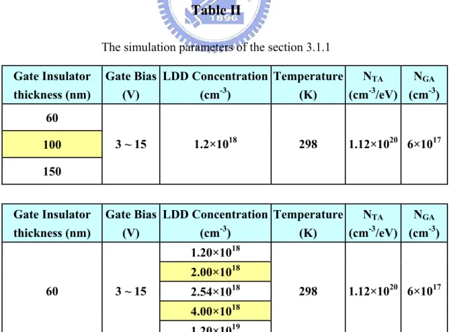
The total simulation various parameters of every section are show in Table II to Table VI. NGA=6×1017cm-3 NTA=1.12×1020cm-3/eV Dens it y of S tat es ( c m -3/e V )
Chapter 3
Results and Discussions
3.1 The Influence Factors on LDD Channel Extension
3.1.1 Gate Insulator Thickness and Bias Voltage
First, base on the simulation parameters which are determined in chapter 2, we change the gate biases from 3 to 15V and gate insulator thicknesses from 60nm to 150nm. The comparison diagram between LDD channel extension length (ΔL) and gate biases with respect to different gate insulator thicknesses is shown in Fig3-1.
Fig.3-1 The influence of gate insulator thickness on the channel extension effect obtained from Silvaco ATLAS simulation with parameters listed in Table II.
NTA = 1.12x1020 cm-3/eV NGA = 6x1017 cm-3 T = 298 K Gate Bias ( V ) 2 4 6 8 10 12 14 16 Δ L ( μ m ) 0.25 0.30 0.35 0.40 0.45 0.50 0.55 0.60 0.65 0.70 60nm 100nm 150nm
Obviously, ΔL and gate biases are positive correlations. However, ΔL and gate insulator thicknesses are negative correlations. The major simulation parameters are shown in Table II.
While the gate bias is arisen, the y-direction vertical electric field between gate and drain is increased. Consequently, the additional gate induced carriers’ region which can regard as the extended channel length is also increased. On account of the same reason, adding the gate insulator thickness causes the vertical electric field is abated and ΔL is decreased.
Second, fix the gate insulator thickness in the initial condition which is 60nm. Change the gate biases from 3 to 15V and change the LDD doping concentration from 1.2×1018 cm-3 to 1.2×1019 cm-3. We can observe that increasing doping concentration causes that ΔL is curtailed, which is shown in Fig3-2.
The influence of gate biases that can affect the vertical electric field has been described previously. Increasing LDD doping concentration can directly reduce the energy barrier height of the grain boundary, and diminish the resistivity of LDD. Therefore, the carriers in the LDD region can overcome the grain boundary barrier and move more easily toward the drain electrode in the horizontal direction. Because of more difficult to keep the carriers in the LDD region near the gate electrode, we will see the ΔL seems to be suppressed.
Fig.3-2 The influence of LDD doping concentration on the channel extension effect obtained from Silvaco ATLAS simulation with parameters listed in Table II.
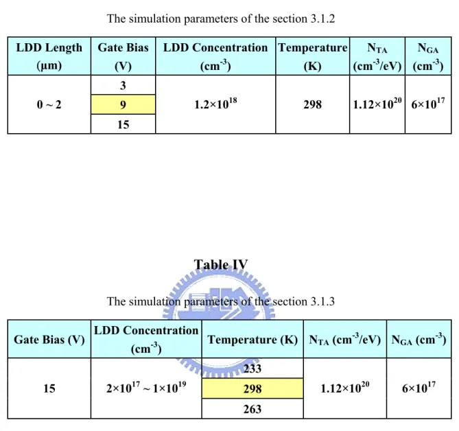
3.1.2 LDD Length
Following the previous simulation manner, the variable which is insulator thickness is replaced by LDD length. And TFTs’ LDD lengths change from 0.5μm, to 2μm inFig.3-3. The major simulation parameters are shown in Table III. As the LDD length is increased, ΔL only increases linearly in the initial regions and achieves respectively saturation values in the longer LDD length regions.
Over the 1μm LDD, the ΔL is saturated. The saturation values are directly equal to the result of 60nm in Fig.3-1 in section 3.1.2. But as LDD less then 1μm, ΔL is limited by the length of LDD region. According to these two trends, the influence of
NTA = 1.12x1020 cm-3/eV NGA = 6x1017 cm-3 T = 298 K Gate Bias ( V ) 2 4 6 8 10 12 14 16 Δ L ( μm ) 0.0 0.2 0.4 0.6 0.8 LDD Concentration = 1.2x1018 cm-3 2.00x10¹⁸ 2.54x10¹⁸ 4.00x10¹⁸ 1.20x10¹⁹
Fig.3-3 The influence of LDD length on the channel extension effect obtained from Silvaco ATLAS simulation with parameters listed in Table III.
the gate voltage can be deduced that the gate bias may only control a limited region around the gate electrode. The effect of different LDD length on ΔL is limited only while the gate voltage is large enough to induce ΔL which is longer then LDD length. Briefly, while the influence of gate bias is large than the length of LDD, the ΔL is limited as the length of LDD, on the contrary, the ΔL will be equal to the result of 60nm in Fig.3-1.
3.1.3 Temperature
When applying the poly-Si TFTs in the circuits, the temperature is also a significant problem. Hence, we vary the LDD doping concentration with the different
NTA = 1.12x1020 cm-3/eV NGA = 6x1017 cm-3 T = 298 K LDD Length ( μm ) 0.0 0.5 1.0 1.5 2.0 2.5 Δ L ( μm ) 0.0 0.1 0.2 0.3 0.4 0.5 0.6 0.7 0.8 VGS= 3V VGS= 9V VGS= 15V
surrounding temperatures which are 233K, 298K, and 363K. The simulation result is showing in Fig.3-4. The major simulation parameters are shown in Table IV. We can observe that when the temperature is increased, ΔL is decreased.
Fig.3-4 The influence of temperature on the channel extension effect obtained from Silvaco ATLAS simulation with parameters listed in Table IV.
In this figure, there are two factors to affect ΔL. The influence of doping concentration has been described in previous 3.1.1 section. The other factor, temperature, will determine the thermal velocity of the carriers. Hence, the carriers are able to own higher thermal energy and thermal velocity when we increase the temperature. The carriers have higher thermal velocity. It means that the carriers spend less time stopping around the dopants and suffer less impurity scattering. The
NTA= 1.12x1020 cm-3/eV NGA= 6x1017 cm-3 VGS= 15V LDD Concentration ( cm-3 ) 1017 1018 1019 Δ L ( μm ) 0.0 0.2 0.4 0.6 0.8 1.0 T = 233K T = 298K T = 363K
carriers have higher thermal energy. In other word, more carriers can overcome the grain boundary barrier. So the carriers can move to drain electrode more quickly and possibly. At the same time, the gate bias will be hardly to keep the carriers. Base on above reasons, ΔL is dominated by thermionic emission effect and impurity scattering effect in temperature response. Hence, we can observe this phenomenon, increasing the surrounding temperature reduces the ΔL.
3.1.4 The Poly-Si Thin Film Property
After discussing about the basic factors, in this section, we will focus on the poly-Si thin film properties in detail. Because this is a n-type TFT, in the density of states (DOS) of the thin film, the main influence on induced carriers’ numbers is acceptor-like state region which is composed by two states which are acceptor-like deep state and acceptor-like tail state. In the Slivaco software, the deep state is assumption as a Gaussian distribution and the tail state is assumption as an exponential distribution. There are two parameters can adjust these two states. One is NGA which specifies the total density of acceptor-like states in a Gaussian distribution,
and unit is cm-3. The other is N
TA which specifies the density of acceptor-like states in
the tail distribution at the conduction band edge, and unit is cm-3/eV. Therefore, we
state in the acceptor-like state of the DOS.
First of all, we fix the NGA which is 6×1017 cm-3, and modify the NTA as
1.12×10¹⁷, 1.12×10¹⁸, and 1.12×1019 cm-3/eV. The major simulation parameters are
shown in Table V. The DOS is shown in Fig.3-5. Again, we change the LDD doping concentration with above three kinds of the DOS to analysis the influence on ΔL, which is shown in Fig.3-6. However, except the effect of doping concentration, the various NTA values seem to only make little variations.
Then, the NTA and NGA exchange for each other. In this time, we fix the NTA
which is 1.12×1020 cm-3/eV, and modify the N
GA as 1×10¹⁷, 3×10¹⁷, 6×10¹⁷ and
1.2×1018 cm-3. The major simulation parameters are shown in Table V. The
simulation result is shown in Fig.3-7. The DOS is shown in Fig.3-8. Although the NGA are different, the effects of doping concentration are all the same: As increasing
the doping concentration, ΔL will be decreased. While exceeding the turning points , ΔL will drop swiftly. Nevertheless, four kinds of NGA values have four respective
critical points. In other words, the critical point and NGA have specific correlation.
According to the mechanism of ΔL explained in the preceding sections, we believe the extended current path from gate channel in LDD region is related to the resistivity of poly-Si thin film.
Fig.3-5 The density of states (DOS). NGA is fixed in 6x1017 cm-3. (a) NTA=1.12x1019 cm-3 , (b) N TA=1.12x1020 cm-3 , (c) NTA=1.12x1021 cm-3 NGA=6×1017cm-3 NTA=1.12×1021cm-3/eV NGA=6×1017cm-3 NTA=1.12×1020cm-3/eV NGA=6×1017cm-3 NTA=1.12×1019cm-3/eV ( a ) ( b ) ( c )
Fig.3-6 The influence of thin film property NTA on the channel extension effect
obtained from Silvaco ATLAS simulation with parameters listed in Table V.
Fig.3-7 The influence of thin film property NGA on the channel extension effect
obtained from Silvaco ATLAS simulation with parameters listed in Table V. VGS= 15V VDS= 0.1V NGA= 6x1017 cm-3 LDD Concentration ( cm-3 ) 1017 1018 1019 Δ L ( μm ) 0.0 0.1 0.2 0.3 0.4 0.5 0.6 0.7 0.8 NTA= 1.12x10 19 NTA= 1.12x10 20 NTA= 1.12x10 21 VGS= 15V VDS= 0.1V NTA= 1.12x1020 cm-3/eV LDD Concentration ( cm-3 ) 1016 1017 1018 1019 Δ L ( μm ) 0.0 0.2 0.4 0.6 0.8 NGA= 1x10 17 NGA= 3x10 17 NGA= 6x10 17 NGA= 1.2x10 18 1×10¹⁷ 4×10¹⁷ 1.2×10¹⁸ 4×10¹⁸
Fig.3-8 The density of states (DOS). NTA is fixed in 1.12x1020 cm-3. (a) NGA=1x10¹⁷
cm-3, (b) N
GA=3x1017 cm-3, (c) NGA=6x1017 cm-3 (d) NGA=1.2x1018 cm-3.
The correlation between resistivity and doping concentration is referred in Seto’s model [17]. Consider the depletion of the grain of poly-Si thin film, the correlation curve is shown in Fig.3-9 which also has a specific turning point at
NGA=3×1017cm-3 NTA=1.12×1020cm-3/eV NGA=6×1017cm-3 NTA=1.12×1020cm-3/eV NGA=1.2×1018cm-3 NTA=1.12×1020cm-3/eV ( a ) ( b ) ( c ) ( d ) NGA=1×1017cm-3 NTA=1.12×1020cm-3/eV
N = Qt / L (1)
where N is the doping concentration and unit is cm-3.
Qt is the deep level trap density of state and unit is cm-2.
L is the average grain length of poly-Si thin film and unit is cm.
Fig.3-9 The correlation between resistivity and doping concentration. [17]
Compared to our study,
GA GA t N L L N L Q N = = × = (2) Therefore, when the LDD doping concentration (N) is equal to NGA, ΔL should be
going to drop rapidly. This assumption is matched perfectly with our simulation results in Fig.3-7.
Now, because of the critical point N = NGA, the Fig.3-7 can be divided into two
regions to discuss. The two regions are the left-hand side N < NGA, and the right-hand
side N > NGA. We transfer the diagram from Fig.3-7 into Fig.3-10. Vary the NGA from
1×1017 cm-3 to 1.2×1018 cm-3 with respect to different doping concentrations (N)
which are 1×10¹⁷, 1.2×10¹⁸, and 4×1018 cm-3. In this figure, the bottom curve is N >
NGA, the top curve is N < NGA, and the central curve is cross the N = NGA point.
Fig.3-10 The influence of LDD doping concentration and NGA on the channel
extension effect obtained from Silvaco ATLAS simulation with parameters listed in Table V.
When N > NGA, according to Seto’s model [17] and R. R. Shah’s research [18],
as the NGA is raised, the difference between N and NGA is going to be less. Hence the VGS= 15V VDS= 0.1V NTA= 1.12x1020 cm-3/eV NGA ( cm-3 ) 1017 1018 Δ L ( μm ) 0.0 0.2 0.4 0.6 0.8 1.0 LDD Conc.= 1.0x10¹⁷ LDD Conc.= 1.2x10¹⁸ LDD Conc.= 4.0x10¹⁸
resistivity and ΔL is increased conspicuously. In brief, the better thin film quality has fewer defects and higher conductivity, therefore has shorter extended channel length. While N < NGA, the minimum NGA has the best thin film quality and the smallest
resistivity, however, it also has the maximum ΔL in our simulation. This result is contrary to our earlier inferences. Clearly, there have other mechanisms which we do not realize to involve in.
Finally, we will additionally study the effect of thin film property on different temperatures. The major simulation parameters are shown in Table VI. In the section 3.1.3, we have proposed that increasing the surrounding temperature reduces the ΔL. In the different thin film properties, this phenomenon is also existence. The results are shown in Fig.3-11 and Fig.3-12. The slope means the various degree of ΔL with respect to different temperatures.
While we adjust the NGA, the slopes are corresponding changed but the changes
do not exist specific trends. In spite of the influence of the NGA on slope does not exist
consistency, the NTA has different effect on slope. As the NTA is arisen, the decay of
ΔL is also raised. The slope is more negative. These results we deduce that the increasing NTA causes the free carriers which is induced by gate voltage become
fewer, so the influence of temperature will be more conspicuously. But why the various NGA does not have the same trend, the reasons we are still researching, now.
Fig.3-11 The influence of temperature and NGA on the channel extension effect
obtained from Silvaco ATLAS simulation with parameters listed in Table VI. (a) VGS=3V (b) VGS=9V (c) VGS=15V VGS= 3V NTA= 1.12x10²⁰ Temperature ( K ) 220 240 260 280 300 320 340 360 380 Δ L ( μ m ) 0.05 0.10 0.15 0.20 0.25 0.30 0.35 Raw Data NGA= 3x10¹⁷ NGA= 6x10¹⁷ NGA= 1.2x10¹⁸ slope = -8.47 x10⁻⁴ slope = -3.35 x10⁻⁴ slope = -3.65 x10⁻⁴ slope = -7.75 x10⁻⁴ VGS= 9V NTA= 1.12x10²⁰ Temperature ( K ) 220 240 260 280 300 320 340 360 380 Δ L ( μ m ) 0.2 0.3 0.4 0.5 0.6 0.7 Raw Data NGA= 3x10¹⁷ NGA= 6x10¹⁷ NGA= 1.2x10¹⁸ slope = -1.20 x10⁻³ slope = -1.14 x10⁻³ slope = -6.17 x10⁻⁴ slope = -7.09 x10⁻⁴ VGS= 15V NTA= 1.12x10 20 Temperature ( K ) 220 240 260 280 300 320 340 360 380 Δ L ( μ m ) 0.4 0.5 0.6 0.7 0.8 Raw Data NGA= 3x10¹⁷ NGA= 6x10¹⁷ NGA= 1.2x10¹⁸ slope = -1.31 x10⁻³ slope = -1.18 x10⁻³ slope = -6.87 x10⁻⁴ slope = -7.75 x10⁻⁴ ( a ) ( b ) ( c )
Fig.3-12 The influence of temperature and NTA on the channel extension effect
obtained from Silvaco ATLAS simulation with parameters listed in Table VI. (a) VGS=3V (b) VGS=9V (c) VGS=15V VGS= 15V NGA= 6x10 17 Temperature ( K ) 220 240 260 280 300 320 340 360 380 Δ L ( μ m ) 0.50 0.55 0.60 0.65 0.70 0.75 0.80 Raw Data NTA= 1.12x10¹⁹ NTA= 1.12x10²⁰ NTA= 1.12x10²¹ slope = -1.31 x10⁻³ slope = -1.18 x10⁻³ slope = -1.26 x10⁻³ slope = -1.58 x10⁻³ VGS= 9V NGA= 6x10¹⁷ Temperature ( K ) 220 240 260 280 300 320 340 360 380 Δ L ( μ m ) 0.35 0.40 0.45 0.50 0.55 0.60 0.65 0.70 Raw Data NTA= 1.12x10¹⁹ NTA= 1.12x10²⁰ NTA= 1.12x10²¹ slope = -1.20 x10⁻³ slope = -1.14 x10⁻³ slope = -1.14 x10⁻³ slope = -1.42 x10⁻³ VGS= 3V NGA= 6x10¹⁷ Temperature ( K ) 220 240 260 280 300 320 340 360 380 Δ L ( μ m ) 0.16 0.18 0.20 0.22 0.24 0.26 0.28 0.30 0.32 0.34 0.36 Raw Data NTA= 1.12x10¹⁹ NTA= 1.12x10²⁰ NTA= 1.12x10²¹ slope = -8.47 x10⁻⁴ slope = -1.00 x10⁻³ slope = -8.40 x10⁻⁴ slope = -7.75 x10⁻⁴ ( a ) ( b ) ( c )
3.2 Optimal LDD Design for Both ON and OFF State
In the section 3.1, we realize that if we want to restrain the LDD channel extension through device fabrication process, we should grow better thin film which exists fewer defects or dope more dopants into the LDD region. However, the quality of thin film is limited by manufacture equipments and technologies. On the contrary, the method of controlling the doping concentration is easier to achieve the goal, reduce the LDD channel extension.
Doping more dopants into the LDD region can reduce the current path extended from gate channel while the TFT is on state. Nevertheless, as the TFT is off state, because of doping more dopants, the parallel electric field between gate and drain electrodes will increase and cause the leakage current arises. This outcome is contradictory to the original LDD’s purpose which is to suppress the leakage current during off state.
Therefore, in this topic, we will research the optimal LDD design for both on and off states by the discussion about the relation between ΔL and the parallel electric field.
3.2.1 Various Poly-Si Thin Film Properties
The Fig.3-13 is the parallel electric field distribution with different LDD doping concentrations which are 1×10¹², 2×10¹³, and 4×1013 cm-3. The gate bias voltage is
constant in -10V. Because of the electric field direction is from drain to gate in the off state, the values are negative. We choose left-hand side maximum values and compare them with the Fig.3-6 and Fig.3-7 inFig.3-14 and Fig.3-15.
Fig.3-13 The parallel electric field distribution of TFT with 1μm LDD under VGS =
-10V. Gate LDD n+ NGA=6×1017cm-3 NTA=1.12×1020cm-3/eV LDD = 1.7E16 LDD = 4.0E18 LDD = 8.0E18 Doping Concentration
Fig.3-14 The comparison between the extension channel length and electric field with respect to different NTA.
Fig.3-15 The comparison between the extension channel length and electric field with respect to different NGA. LDD Concentration ( cm-3 ) 1016 1017 1018 1019 Δ L ( μm ) 0.0 0.2 0.4 0.6 0.8 NGA=1x10¹⁷ (VGS=15V) NGA=3x10¹⁷ (VGS=15V) NGA=6x10¹⁷ (VGS=15V) NGA=1.2x10¹⁸ (VGS=15V) E F ield ( V/cm ) 20x103 30x103 40x103 50x103 60x103 70x103 80x103 90x103 100x103 NGA=3x10¹⁷ (VGS= -10V) NGA=6x10¹⁷ (VGS= -10V) NGA=1.2x10¹⁸ (VGS= -10V) VDS= 0.1V NTA= 1.12x1020 cm-3/eV VDS= 0.1V NGA= 6x1017cm-3 LDD Concentration ( cm-3 ) 1017 1018 1019 E F iel d ( V/ cm ) 20x103 30x103 40x103 50x103 60x103 70x103 80x103 90x103 100x103 NTA=1.12x10 19 (VGS= -10V) NTA=1.12x10 20 (VGS= -10V) NTA=1.12x10 21 (VGS= -10V) Δ L ( μm ) 0.0 0.1 0.2 0.3 0.4 0.5 0.6 0.7 0.8 NTA=1.12x10 19 (VGS= 15V) NTA=1.12x10 20 (VGS= 15V) NTA=1.12x10 21 (VGS= 15V)
Through the Fig.3-14 and Fig.3-15, we can point out the optimal LDD design criterion for both on and off states. For example, in our device, the optimal LDD doping concentration is located on about 3×1018 cm-3. It is clear that in the optimal
doping concentration, the TFT devices have the shorter extended channel and the lower parallel electric field. We can through this comparison to get the balance between these two problems which are channel extension and leakage current at the same time.
3.2.2 GOLD Structure TFT
Furthermore, in the end of section 3.2, we are interested in the gate overlapped LDD (GOLD) TFTs’ structure which can effectively suppress the leakage current. The overlapped LDD length is 1μm, and none extra LDD structure over out the gate channel. The structure, net doping profile, current density distribution, surface current density distribution, and parallel electric field distribution are shown in Fig.3-16 to Fig.3-19. The gate bias is constant in 15V during on state, and in -10V during off state. The overlapped LDD concentration is from 1×10¹⁷ to 1×1019 cm-3. We can see that
the surface current density will drop quickly in the GOLD region as the doping concentration is too large. It perhaps reduces the effective channel length and derogates the performance of the TFTs. The comparison between ΔL and the parallel
electric field, the result is shown in Fig.3-20. Obviously, ΔL in the GOLD structure is almost equal to zero. The GOLD TFTs is an excellent structure to suppress the leakage current and LDD channel extension.
Fig.3-16 The net doping profile of the GOLD structure.
Fig.3-17 The current density distribution of the GOLD structure.
Lateral Position (μm)
Vertica
l P
osi
ti
on (
μ
m)
GOLD
n
+Lateral Position (μm)
Vertical P
osit
io
n (
μ
m)
GOLD
n
+Fig.3-18 The surface current density distribution of the GOLD structure.
Fig.3-19 The X direction E field distribution of the GOLD structure.
Lateral Position (μm)
C
u
rrent Density
( A
/cm
2)
Channel GOLD
n
+ GOLD = 1.7E16 GOLD = 1.2E18 GOLD = 2.0E18 GOLD = 4.0E18 Doping ConcentrationLateral Position (μm)
E Fi
eld ( V/
cm
)
Channel GOLD
n
+ Doping ConcentrationFig.3-20 The GOLD structure’s comparison between the extension channel length and electric field with respect to different NGA.
VDS= 0.1V NTA= 1.12x1020 cm-3/eV LDD Concentration ( cm-3 ) 1017 1018 1019 Δ L ( μm ) 0.000 0.005 0.010 0.015 0.020 0.025 0.030 NGA= 3x10 17 (VGS=15V) NGA= 6x10 17 (VGS=15V) NGA= 1.2x10 18 (VGS=15V) E Fie ld ( V/c m ) 0 20x103 40x103 60x103 80x103 NGA= 3x10 17 (VGS=-10V) NGA= 6x10 17 (VGS=-10V) NGA= 1.2x10 18 (VGS=-10V)
Chapter 4
Conclusion
In this thesis, we present the influence factors on LDD channel extension and purpose the optimal LDD design for both on and off states by way of the simulation software, Silvaco.
First, we discuss several influence factors, such as gate insulator thickness, LDD length, bias voltage, temperature and poly-Si thin film property. However, these factors almost are around two main issues. One is the vertical electric field between gate and drain electrodes, and the other is the resistivity of Lightly Doped Drain. The vertical electric field can induce the carriers and keep them to form the extended current path. The channel extension effect is dominated by the vertical electric field. However, while the LDD length is not long enough, the extended channel length will be limited by LDD length. Moreover, the channel extension is regarded as the channel length of the parasitic transistor and the parasitic transistor is also dominated by thermionic emission effect in temperature response. The other issue is the resistivity of LDD. According to the Seto’s model, as doping concentration is increased and larger than NGA, the resistivity of LDD will be decreased. Because of decreasing the resistivity, it
can form the extended channel. It coincides with our simulation results perfectly. While the doping concentration is large than NGA, the extended channel length is
dropped swiftly. Hence, we deduce the resistivity of the thin film is the other main issue to influence on LDD channel extension effect.
Second, doping more dopants into the LDD region can suppress the channel extension. However, it also increases the parallel electric field and leakage current. Here, we give a notion to design the optimal LDD. Through a comparison between channel extension length and parallel electric field, we can point out the optimal LDD design criterion which has the shorter extended channel length during on state and less leakage current during off state.
Finally, the proposed LDD channel extension factors’ influences are established basing on the simulation and the assumptions mentioned above. Our research results provide some factors and an approach which can be the reference and help improve the electric characteristics of the devices for all poly-Si thin film TFTs with LDD structure.
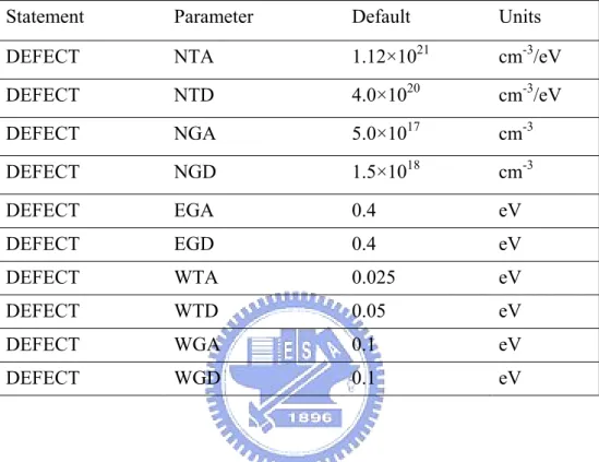
Appendix A
Density of States Model in Silvaco
It is assumed that the total density of states (DOS) and g(E), is composed of four bands: two tail bands (a donor-like valence band and an acceptor-like conduction band) and two deep level bands (one acceptor-like and the other donor-like) which are modeled using a Gaussian distribution.
) ( ) ( ) ( ) ( ) (E g E g E g E g E g = TA + TD + GA + GD (A-1) Here, E is the trap energy, EC is the conduction band energy, EV is the valence band
energy and the subscripts (T, G, A, D) stand for tail, Gaussian (deep level), acceptor and donor states respectively.
(A-2)
(A-3) (A-4) (A-5) For an exponential tail distribution, the DOS is described by its conduction and valence band edge intercept densities (NTA and NTD), and by its characteristic decay energy (WTA and WTD). For Gaussian distributions, the DOS is described by its total density of states (NGA and NGD), its characteristic decay energy (WGA and
WGD), and its peak energy/peak distribution (EGA and EGD). Table A shows the user-specifiable parameters for the density of defect states [19].
Table A. User-Specifiable Parameters for Equations A-2 to A-5 Statement Parameter Default Units DEFECT NTA 1.12×1021 cm-3/eV DEFECT NTD 4.0×1020 cm-3/eV DEFECT NGA 5.0×1017 cm-3 DEFECT NGD 1.5×1018 cm-3 DEFECT EGA 0.4 eV DEFECT EGD 0.4 eV DEFECT WTA 0.025 eV DEFECT WTD 0.05 eV DEFECT WGA 0.1 eV DEFECT WGD 0.1 eV
Appendix B
Temperature Correlation Equations
Trapped Carrier Density
The ionized densities of acceptor and donor like states (nT and pT respectively)
are given by:
GA TA T p p p = + (B-1) GD TD T n n n = + (B-2)
where nTA, nGA, pTD and pGD are given below.
(B-3)
(B-4)
(B-5)
ftTA(E, n, p) and ftGA(E, n, p) are the ionization probabilities for the tail and Gaussian
acceptor DOS, while ftTD(E, n, p) and ftGD(E, n, p) are the ionization probabilities
for the donors.
In the steady-state case, the probability of occupation of a trap level at energy E for the tail and Gaussian acceptor and donor states are given by Equations B-7 through B-10.
(B-7)
(B-8)
(B-9)
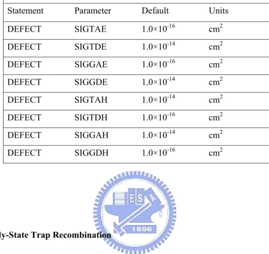
(B-10)
where vn is the electron thermal velocity and vp is the hole thermal velocity, ni is the
intrinsic carrier concentration. SIGTAE and SIGGAE are the electron capture cross-section for the acceptor tail and Gaussian states respectively. SIGTAH and SIGGAH are the hole capture cross-sections for the acceptor tail and Gaussian states respectively and SIGTDE, SIGGDE, SIGGDH, and SIGGDH are the equivalents for
donors states [19].
Steady-State Trap Recombination
For steady-state conditions, the net recombination/generation rate is identical for electrons (Rn) and holes (Rp) (i.e., instantaneous equilibrium). Using Equations B-7
through B-10 to give the values of ftand following the derivation by Shockley and Read [20] and Hall [21], the Shockley-Read-Hall recombination/generation rate due to the defect states is given by: [19]
Table B-1. User-Specifiable Parameters for Equations B-7 to B-10 Statement Parameter Default Units
DEFECT SIGTAE 1.0×10⁻¹⁶ cm2 DEFECT SIGTDE 1.0×10⁻¹⁴ cm2 DEFECT SIGGAE 1.0×10⁻¹⁶ cm2 DEFECT SIGGDE 1.0×10⁻¹⁴ cm2 DEFECT SIGTAH 1.0×10⁻¹⁴ cm2 DEFECT SIGTDH 1.0×10⁻¹⁶ cm2 DEFECT SIGGAH 1.0×10⁻¹⁴ cm2 DEFECT SIGGDH 1.0×10⁻¹⁶ cm2
(B-11)
Transient Traps
For the transient case, time is required for carriers to be emitted or captured and therefore instantaneous equilibrium cannot be assumed. This means that Equation B-11 is no longer valid for transient simulations. Instead, the total recombination/generation rate for electrons (which is equal to electron recombination rate minus the generation rate for electrons) is calculated using the transient probabilities of occupation for acceptors (ftTA and ftGA). These are calculated by
solving additional rate equations (Equations B-12 and B-13).
(B-13)
The total hole recombination/generation rate can also be determined from the transient values of ftTD and ftGD (see Equations B-14 and B-15).
(B-14)
(B-15)
A transient trap simulation using this model is more time consuming than using the static model but gives a much more accurate description of the device physics. It may sometimes be acceptable to perform transient calculations using the static trap distribution and assume that traps reach equilibrium instantaneously [19].
References
[1] A. G. Lewis, I-W. Wu, T. Y. Huang, A. Chiang, and R. H. Bruce, “Active matrix liquid crystal display design using low and high temperature processed polysilicon TFTs,’’ in IEDM Tech. Dig., pp. 843-846, 1990
[2] Y. Matsueda, M. Ashizawa, S. Aruga, H. Ohshima, and S. Morozumi, “New technologies for compact TFT LCDs with high-aperture ratio, ’’soc. Information Display, Tech. Dig., pp. 315-318, 1990.
[3] R. G. Stewart, S. N. Lee, A. G. Ipri, D. L. Jose, D. A. furst, S. A. Lipp, and W. R. Roach, “A 9V polysilicon LCD with integrated gray-scale drivers,” soc. Information Display, Tech. Dig., pp. 319-322, 1990.
[4] T. Yamanaka, T. Hashimoto, N. Hasegawa, T. Tanaka, N. Hashimoto, A. Shimizu, N. Ohki, K. Ishibashi, K. Sasaki, T.Nishida, T. Mine, E. Takeda, and T. Nagano, ”Advanced TFT SRAM Cell Technology Using a Phase-Shift Lithography,’’ IEEE Trans. Electron Devices, Vol. 42, No. 7, pp. 1305-1313, 1995. [5] S. D. S. Malhi, H. Shichijio, S.K. Banerjee, R. Sundaresan, M. Elahy, G. P. Polack, W. F. Richardaon, A. h. Shah, L. R. Hite, R. H. Womoack, P. K. Chatterjee, and H. W. Lan, “Characteristics and Three-Dimensional Integration of MOSFETs in Small-Grain LPCVD Polycrystalline Silicon,’’ IEEE Trans. Electric Devices, Vol. 32, No. 2, pp. 258-281, 1985.
[6] K. YoShizaki, H. Takahashi, Y. Kamigaki, T.Yasui, K. Komori, and H. Katto, ISSCC Digest of tech. Papers, pp. 166, 1985.
[7] N. D. Young, G. Harkin, R. M. Bunn, D. J. McCullloch, and I.D. French, “The Fabrication and Characterization of EEPROM Arrays on Glass Using a Low-Temperature Poly-Si TFT Process,’’ IEEE Trans. Electron Devices, Vol. 43, No.11, pp. 1930-1936, 1996.
[8] T. Kaneko, Y. Hosokawa, M. Tadauchi, Y. Kita, and H. Andoh, “400 dpi Integrated Contact Type Linear Image Sensors with poly-Si TFT’s Analog Readout Circuits and Dynamics shift Registers,” IEEE Trans. Electron Devices, Vol. 38, No. 5 ,pp. 1086-1039, 1991.
[9] Y. Hayashi, H. Hayashi, M. Negishi, T. Matsushita, “A Thermal Printer Head with CMOS Thin-Film Transistors and Heating Elements Integrated on a Chip,’’ IEEE Solid-State Circuits Conference (ISSCC), pp. 266, 1998.
[10] N. Yamauhchi, Y. Inaba, and M. Okamamura, “An Integrated Photodector-Amplifier using a-Si p-i-n Photodiodes and Poly-Si Thin Film Transistors, ’’ IEEE Photonic Tech. Lett., Vol. 5, pp. 319, 1993.
[11] M. G. Clark, “Current status and future prospects of poly-Si devices,” IEE Proceedings-Circuits, Devices and Systems, vol. 141, pp. 3-8, 1994.
[12] S. D. S. Malhi, H. Shichijio, S. K. Banerjee, R. Sundaresan, M. Elahy, G. P. Polack, W. F. Richardaon, A. H. Shah, L. R. Hite, R. H. Womoack, P. K. Chatterjee and H. W. Lan, “Characteristics and Three-Dimensional Integration of MOSFETs in Small-Grain LPCVD Polycrystalline Silicon,” IEEE Trans. Electron Devices, Vol. 32, No. 2, pp. 258-281, 1985.
[13] T. Serikawa, S. Shirai, A. Okamoto and S. Suyama,“Low-temperature fabrication of high-mobility poly-Si TFTs for large-area LCDs,” IEEE Trans. Electron Devices, Vol. 36, pp. 1929-1933, 1989.
[14] K. R. Olasupo and M. K. Hatalis, IEEE Trans. Electron Devices, Vol. 43, pp. 1218, 1996.
[15] C. Liu, C. D. Yu, A. Kornbilt, and K. Lee, IEEE Trans. Electron Devices, Vol. 39, pp. 2803, 1992.
[16] Hsiao-Wen Zan and Kuang-Ming Wang, “The Channel Length Extension in Poly-Si TFTs with LDD Structure,” IEEE Device Letters has be published.
[17] John Y. W. Seto, J. Appl. Phys., Vol. 46, pp. 5247-5254, 1975.
[18] Dae M. Kim, A. N. Khondker, S. S. Ahmed, and Rajiv R. Shah, IEEE Trans. Electron Devices, Vol. 31, pp. 480-493, 1984.
[20] Shockley W., and W.T. Read, “Statistics of the Recombination of Holes and Electrons”, Phys. Rev.87 (1952): 835-842.
[21] Hall, R.N., “Electron Hole Recombination in Germanium”, Phys. Rev. 87 (1952): 387.
Table I
The brief specification of the poly-Si TFTs
Name Material Thickness Active Layer Poly-Si 50 nm
SiOX 50 nm
Gate Insulator
SiNX 20 nm
Table II
The simulation parameters of the section 3.1.1
Gate Insulator thickness (nm) Gate Bias (V) LDD Concentration (cm-3) Temperature (K) NTA (cm-3/eV) NGA (cm-3) 60 100 150 3 ~ 15 1.2×10¹⁸ 298 1.12×10²⁰ 6×10¹⁷ Gate Insulator thickness (nm) Gate Bias (V) LDD Concentration (cm-3) Temperature (K) NTA (cm-3/eV) NGA (cm-3) 1.20×10¹⁸ 2.00×10¹⁸ 2.54×10¹⁸ 4.00×10¹⁸ 60 3 ~ 15 1.20×10¹⁹ 298 1.12×10²⁰ 6×10¹⁷ Name Material Doping Concentration LDD ( n- ) 1.2 x 1018 cm-3
n+ Phosphorus 2.0 x 1020 cm-3
W/L = 6μm / 6μm Average Grain Size = 0.8μm
Table III
The simulation parameters of the section 3.1.2
LDD Length (μm) Gate Bias (V) LDD Concentration (cm-3) Temperature (K) NTA (cm-3/eV) NGA (cm-3) 3 9 0 ~ 2 15 1.2×10¹⁸ 298 1.12×10²⁰ 6×10¹⁷
Table IV
The simulation parameters of the section 3.1.3
Gate Bias (V) LDD Concentration
(cm-3) Temperature (K) NTA (cm -3/eV) N GA (cm-3) 233 298 15 2×10¹⁷ ~ 1×10¹⁹ 263 1.12×10²⁰ 6×10¹⁷
Table V
The simulation parameters of the section 3.1.4
Gate Bias (V) LDD Concentration
(cm-3) Temperature (K) NTA (cm -3/eV) N GA (cm-3) 1.12×10¹⁹ 1.12×10²⁰ 15 2×10¹⁷ ~ 1×10¹⁹ 298 1.12×10²¹ 6×10¹⁷
Gate Bias (V) LDD Concentration
(cm-3) Temperature (K) NTA (cm -3/eV) N GA (cm-3) 1×10¹⁷ 3×10¹⁷ 6×10¹⁷ 15 2×10¹⁷ ~ 1×10¹⁹ 298 1.12×10²⁰ 1.2×10¹⁸
Table VI
The simulation parameters of the various temperatures in section 3.1.4
Gate Bias (V) LDD Concentration
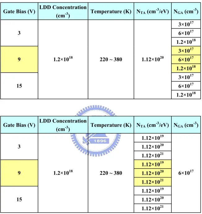
(cm-3) Temperature (K) NTA (cm -3/eV) N GA (cm-3) 3×10¹⁷ 6×10¹⁷ 3 1.2×10¹⁸ 3×10¹⁷ 6×10¹⁷ 9 1.2×10¹⁸ 3×10¹⁷ 6×10¹⁷ 15 1.2×10¹⁸ 220 ~ 380 1.12×10²⁰ 1.2×10¹⁸
Gate Bias (V) LDD Concentration
(cm-3) Temperature (K) NTA (cm -3/eV) N GA (cm-3) 1.12×10¹⁹ 1.12×10²⁰ 3 1.12×10²¹ 1.12×10¹⁹ 1.12×10²⁰ 9 1.12×10²¹ 1.12×10¹⁹ 1.12×10²⁰ 15 1.2×10¹⁸ 220 ~ 380 1.12×10²¹ 6×10¹⁷