國
立
交
通
大
學
電機資訊學院 電子與光電學程
碩
士
論
文
在高電漿密度蝕刻機中 SF
6電漿分解產物對產品的影
響與研究
Study of SF
6
Decomposition Products
of DPS Poly Etcher in IC’s
Manufacturing
研 究 生:許時齊
指導教授:張國明 教授
在高電漿密度蝕刻機中 SF
6電漿分解產物對產品的影
響與研究
Study of SF
6Decomposition Products of DPS
Poly Etcher in IC’s Manufacturing
研 究 生:許時齊 Student:Shih-Chi Hsu
指導教授:張國明 Advisor:Kow-Ming Chang
國 立 交 通 大 學
電機資訊學院 電子與光電學程
碩 士 論 文
A Thesis
Submitted to Degree Program of Electrical
Engineering Computer Science
College of Electrical Engineering and Computer
Science
National Chiao Tung University
in Partial Fulfillment of the Requirements
for the Degree of
Master of Science
in
Electronics and Electro-Optical Engineering
June 2004
Hsinchu, Taiwan, Republic of China
中華民國九十三年六月
在高電漿密度蝕刻機中 SF
6電漿分解產物對產品的影響與研究
學生 : 許時齊 指導教授 : 張國明博士 國立交通大學 電子工程學系 碩士在職專班摘要
本論文研究分為兩大主題: 第一個主題是研究 SF6 電漿分解產物所污染的環境對金屬腐蝕所產生的影響。由實 驗中得知經過 SF6電漿分解產物所污染的晶圓盒,容易對金屬產生腐蝕作用。在 IC 製 造的工廠中,金屬腐蝕所造成的產品品質問題常常困擾著許多人。而如何造成金屬腐蝕 及如何解決也是眾說紛紜。因為金屬腐蝕常常發生在不固定的地方及不固定的時間,也 沒有規律性可言。本研究發現金屬腐蝕來自 SF6電漿分解產物所污染的晶圓盒。SF6電 漿分解產物中的 SF5 或 SF4 容易吸附在晶圓盒的表面,與空氣中的水氣反應後產生腐 蝕性的氫氟酸,氫氟酸非常容易與鋁金屬反應形成三氟化鋁。 所以晶圓承載盒在晶圓 製造的過程中常常是污染源。 第二個主題是研究在雙源電漿蝕刻機中,SF6 電漿分解產物形成半透明的六角形微 粒污染晶圓。而化合物“F11NS2” (or (F5S)2NF) 是最有可能的生成物,具有揮發特性。在 雙源電漿蝕刻機中,SF6電漿分解產物中的 SF5 與三氮化矽形成化合物,附著於晶圓表 面。而加入氧電漿於蝕刻後可有效去除此種微粒,因為氧電漿可以有效的降低 SF5 的濃 度,進而降低微粒的形成。最後結論,我們探討的主題放在未來要如何避免蝕刻副產物所造成的晶圓交互污 染。利用各種設計,來降低所有可能的污染途徑。有許多的想法已經施行於現有的機台 上許多年,且得到很好的成果。
Study of SF
6Decomposition Products of DPS poly etcher in IC’s
Manufacturing
Student : Shih-Chi Hsu Advisor : Dr. Kow-Ming Chang
Institute of Electronics National Chiao Tung University
Abstract
In this thesis, there are two topics of SF6 decomposition products of DPS poly etcher in
IC’s manufacturing to be studied. One is the study of metal corrosion in an environment contaminated with SF6 decomposition products. The other is the study of contamination of
SF6 plasma decomposition in DPS poly dry etcher.
The first topic is about the corrosion metal. It was found interesting that the metal corrosion have strong correlation with environment contaminated with SF6 decomposition
products. In IC’s manufacturing, the corrosion metal appeared sometime and somewhere, the period was irregularly, and suffered many companies for a long time. The corrosion Al-Cu film is caused by SF5 or SF4 of SF6 decomposition. SF5 or SF4 absorbs on the surface of box
and react with moisture. HF is existence on the boxes, attacks metal film and causes corrosion metal.
The second topic is the reduction of semi-translucent hexagonal defect from SF6
compound of the volatile residue. Semi-translucent hexagonal defect was formed on nitride wafer in DPS poly etcher with SF6 plasma. Adding O2 plasma treatment in the end of poly
etching is the best solution to remove particle. O2 plasma treatment can decrease of SF5, and
then decrease of F11NS2.
In conclusion, we also prepare some suggestions to avoid cross-contamination in etching area of IC’s manufacturing. Most of suggestions have been implemented in current manufacturing and get good performance.
Acknowledgement
I would like to express sincere gratitude to my advisor, Dr. Kuo Ming Chang for their instruction, encouragement, and insightful suggestion. I learned from him not only the knowledge about semiconductor manufacture but also the appropriate attitude toward researches. Without his detailed advice, this thesis could not be finished successfully.
Appreciation is extended to my colleagues Chih-Hsiang Yung, Gordon Chen, Yu-Ching Lin for their technical assistance. Furthermore, the encouragement from my friends Y.H. Huang, Feng-Yi Chen, Cheng-Kang Lin, Peter Chen is highly appreciated.
Finally, I wish to express my deepest gratitude to my wife, parents and children (Lisa and Scott) for their endless love, patient, and spiritual support during the time of my study in the Chiao Tung University.
Contents
Chinese Abstract………. i
English Abstract……… iii
Acknowledgement………..v
Contents……….vi
Table Captions………..vii
Figure Captions………viii
Chapter 1 Introduction………1
Chapter 2 Metal Corrosion in an Environment Contaminated with SF6 Decomposition products 2.1 Introduction of Metal Corrosion………...3
2.2 The Problem and Experiment………5
2.2.1 The Problem………...5
2.2.2 Experiment and Result……….. 7
2.3 Analysis………9
2.4 Conclusion………..11
Chapter 3 Contamination of SF6 Plasma Decomposition in DPS Poly Etcher 3.1 Introduction of DPS Poly Etcher………13
3.2 The Problem and Experiment……….14
3.3 Analysis………...16
3.4 Conclusion………..18
Chapter 4 Conclusion and Suggestion for Future Work………...20
Table Captions
Figure Captions
Fig 2.1 Wafer map of metal corrosion inspected by KLA TENCOR tools, KLA map of slot 1,11,25 in whole cassette of 25 wafers………...26 Fig 2.2 The pictures of corrosion metal, the top picture inspected by optical microscope (OM), the others inspected by second electron microscope (SEM)………..27 Fig 2.3 Corrosion metal appeared all kinds of metal etchers, post clean processes, metal
sputtering deposition, photoresist coater, photoresist exposure in all time…………28 Fig 2.4 Corrosion metal was composed of aluminum, oxygen and fluorine by EDX………..29 Fig 2.5 Corrosion metal wasn’t eliminated after metal etching back again………..29 Fig 2.6 Wafer A – just metal etched and didn’t asher, the KLA map appeared metal corrosion on All wafer. This type corrosion metal was composed of chlorine, oxygen and aluminum; also inspected by SEM (second electron microscope)………30 Fig 2.7 The KLA maps of “wafer B – wafer held with cassette in open area” and “wafer C – wafer held with cassette in clean box”. Didn’t find corrosion metal on all wafers..30 Fig 2.8 Wafer D – wafer held with cassette in contaminated fluoride box, the KLA map
appeared metal corrosion on top/bottom of wafer. This type corrosion metal was composed of fluorine, oxygen and aluminum; also inspected by SEM (second electron microscope)………..31 Fig 2.9 Wafer E – box be contaminated with SF6 high density plasma of poly etcher, there
were serious metal corrosion on wafer. Inspected by SEM and composed of aluminum, oxygen, fluorine by EDX……….31 Fig 2.10 Wafer F – box be contaminated with NF3 high density plasma of poly etcher, there
were metal corrosion on wafer. Inspected by SEM and composed of aluminum, oxygen, fluorine by EDX………..32 Fig 2.11 Wafer maps of wafer G – box be contaminated with NF3 median density plasma of
poly etcher, wafer H – box be contaminated with C4F8 high density plasma of oxide
etcher, wafer I -- box be contaminated with C4F8 median density plasma of oxide
etcher; we couldn’t find any corrosion on three types of boxes………….…………..32
Fig 2.12 In order to avoid contamination of metal, dedicated special boxes for metal wafer transport is a must………..33
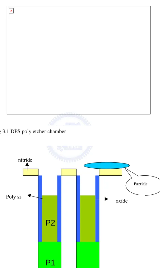
Fig 3.1 DPS poly etcher chamber……….34
Fig 3.2 Wafer structure, isotropic dry etching to define poly 2 depth at this step………34
Fig 3.3 Semi-translucent hexagonal defect on the wafer by KLA inspected………35
Fig 3.4 The efficiency of particle reduction with SPM + APM. The left lot – defect counts reduce from 1253 to 25 at 1st time clean. The right lot – defect counts reduce from 21762 to 300 at the 1st time and to 21 at the 2nd time clean………...36
Fig 3.5 The efficiency of particle reduction with SPM + APM once and twice………...36
Fig 3.6 The result of adding N2 plasma treatment in the end of poly etching………..37
Fig 3.7 The result of adding O2 plasma treatment in the end of poly etching. The removed efficiency is good for treatment 5, 10, 15 seconds………37
Fig 3.8 The O2 plasma treatment don’t influence poly etching performance. The depth is stable in different treatment time………..38
Chapter 1
Introduction
As semiconductor devices continue to be highly integrated and their geometries also continue to shrink, not only particulate and metallic contaminants but also trace contamination from process by-product on the surface of silicon wafers have been found to have an increasingly detrimental impact on the performance and yield of semiconductor products. In this paper, when silicon wafers are exposed to the atmosphere in a conventional clean room, gaseous molecules of process by-product in the air easily adsorb onto the surfaces of the silicon wafers in a short time. The fluorine molecules are easy to induce metal corrosion and surface particle.
A cleanroom is a man-made environment that has much lower particle counts than the normal environment. Standard definitions of cleanroom classifications are a strange combination of metric and English units. A class 1 cleanroom must achieve less than 1 particle with diameter larger than 0.5um per cubic foot. Particles can cause many different defects. For instance, particles on the clear area of mask or reticle can cause pinhole for negative photoresist or stumps for positive photoresist during the photolithography process. During etch process, those pinholes and stumps are transferred to the wafer surface and cause defects. It is very important to maintain a rigid cleanroom protocol to minimize the yield loss due to the contamination. But it is difficult to control the contamination come from gaseous molecules of process by-product.
SF6 gas used to playing an important part in plasma dry etching chemistry, many poly
etchings and tungsten etchings have been used. In this thesis, there are two topics of SF6 gas
corrosion in an environment contaminated with SF6 decomposition products. The other is the
study of contamination of SF6 plasma decomposition in DPS poly dry etcher. The thesis was
organized as follow:
Chapter 1 – Started with a brief introduction and background description.
Chapter 2 – We discussed the metal corrosion in an environment contaminated with SF6
decomposition products. A brief introduction of metal corrosion had been reported and illustrated the experiment preparation of metal corrosion by fluorine residues. Finally, explained the mechanism of fluorine residues inducing metal corrosion by SF6 plasma
decomposition.
Chapter 3 – we discussed the contamination of SF6 plasma decomposition in DPS Poly etcher.
A brief introduction of DPS poly etcher had been reported. Describing in detail about the particle contamination of SF6 plasma decomposition in DPS poly etcher and trying many
methods to eliminate it. The “F11NS2” ( or (F5S)2NF ) is the most possible compound in the volatile residue. The reason was (F5S)2NF needs nitrogen source to react with SF6 and SF5,
that may explain we never saw volatile particle on oxide particle monitor wafer. The slow SiN etch rate we should not expect the compound of high nitrogen ratio form during process. (So, F2N2S3 and F4N4S4 is not good guess).
Chapter 4 – finally, some conclusions were summarized and some future work was proposed in this chapter.
Chapter 2
Metal Corrosion in an Environment Contaminated with SF
6Decomposition Products
2.1 Introduction of Metal Corrosion
Al-based metals have been adopted as interconnection materials in semiconductor devices. In particular, Al-Cu alloys are used widely for ultra large scale integration circuits (ULSI). Adding a small amount of Cu to an Al film builds up its electromigration resistance and mechanical strength, and suppresses hillock formation. However, Cu addition to Al also reduces corrosion resistance for some acids. Corrosion is one of the most serious problem in Al dry-etching technology. Al-Cu corrosion produces serious problem of device performance and long-term reliability.
Corrosion is defined as metal loss or deterioration due to oxidation. Corrosion can be divided into two broad categories, each with numerous specific examples. The first is general, or macroscopic, corrosion. This is typified by wet etchants used in the past to etch aluminum, or certain types of photo-resist developers currently in use[1,2]. In this case the film is evenly attacked, and if left in the etchant for long enough it would be totally removed. The second type of corrosion, specific, or microscopic, this results in uneven pitting of the surface. This is electrochemical in nature and once the electrochemical potential is removed, the corrosion stops.
Corrosion in solvent strip can occur at four different points during the wet strip process. The first is related to incoming wafer quality. Fluorides and chlorides trapped in the sidewall polymers that form during plasma etching can become activated during wet processing and
cause corrosion. This problem is best resolved by using proper etching chemistries and post etching passivation. Ashing just after the etch step and/or a water rinse and dry are common passivation schemes.
The second macroscopic area of corrosion is during the solvent strip portion of the cycle. Some types of solvents are less prone to metal attack. Amine and hydroxylamine base strippers are less prone to corrode metal than sulfonic acid based strippers[3]. Another more subtle example of this is the interaction between the complicated metal stacks and solvent used to strip them. Metal stacks with un-reacted titanium in them appear to be especially prone to this problem.
The third potential area of corrosion happens during the transition from the solvent strip step to the DI rinse portion of the process. It is well documented that a potential for severe corrosion exists when residual stripper on the wafer surface is mixed with water. The amines react with water to form hydroxyl ions that attack the metal layers.[4] This is a form of macroscopic corrosion, which can be severe but is easily prevented.
The final type of corrosion is perhaps the hardest to prevent. This is the corrosion that happens during the final water rinse. This is almost always electro-chemical in nature. Metal lines typically are aluminum with small amounts of copper and silicon in them. The copper trends to precipitate out into grain boundaries and form copper rich areas. Any time two dissimilar metal are in contact with each other an electro-chemical cell is established. Immersing the cell is an electrolyte completes the circuit and allows corrosion to take place[5][6]. The aluminum is corroded away near the copper rich area until the copper precipitate is isolated, or the cell is removed from the water. This is an example of microscopic corrosion.[i7]
In general ,the corrosion Al-Cu film is caused by the chemical reaction of chlorine residue after dry etching using chlorinated gases. Therefore the removal of chlorine components is important for reducing corrosion. Some treatments for reducing the corrosion of Al-based metallization layers have been investigated. The effects of treatment by exposure to fluorocarbon plasma, and H2O plasma, annealing and oxidation were reported.
In this paper, we report another type of Al-Cu film corrosion. The corrosion Al-Cu film is caused by the chemical reaction of fluoride residue in a specific environment. The corrosion appears on the Al-Cu surface. We discuss the new type of corrosion mechanism in this condition and study the method of prevention in IC’s manufacturing.
2.2 The Problem and Experiment
2.2.1 The Problem
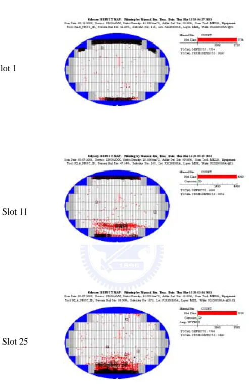
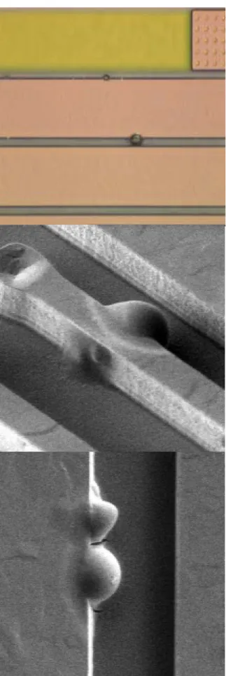
In IC’s manufacturing, the corrosion Al-Cu film is happened irregular and inspected by KLA TENCOR tools. Figure 2.1 shows the corrosion wafer map of slots 1,11,25 in whole cassette of 25 wafers. The corrosion appeared seriously on top/bottom of wafer and Slot 25 was lighter than the others. In manufacturing, the corrosion metal appeared sometime and somewhere, the period was irregular. Figure 2.2 shows the pictures of corrosion metal by optical microscope inspection (OM) and second electron microscope inspection (SEM). The most striking feature in these micrographs is the presence of small raised bump in the border of metal line.
“How to find the root cause ?” had greatly perplexed many IC’s manufacturing fabrications for a long time. We had tried several skills that used to identify uncertain events
quickly in manufacturing for several years to find the root cause.
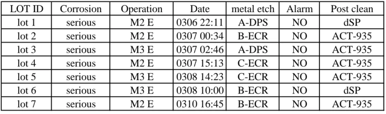
(a) Tool/process correlation : This is well-known method to find a slight difference between different tools or process. What induced the corrosion metal ? From previous introduction, the cause of corrosion may come from metal film sputter, photoresist develop, metal etching or post clean. Figure 2.3 shows the corrosion appeared all kinds of metal etchers, post clean process, metal sputtering deposition, photo-resist coater, photo-resist exposure in all time. The corrosion appeared two kinds of metal etcher, ECR and DPS at the same time. The post clean process of metal etching was also including two typical processes, ACT-935 amine base stripper and dSP dilute solfonic acid. Unfortunately, no evidences could correlate the corrosion with each process or tool.
(b) It is important that chlorine residue must be carried out in photo-resist stripping after metal etching. In order to remove chlorine residue, H2O/O2 plasma be implemented in
DPS metal etcher and CH3OH/O2 plasma be implemented in ECR Hitachi metal etcher. In
that corrosion period, the asher rate was normal and stable in both of tools. Therefore, all of the subsystems were stable, temperature controller, pressure controller, mass flow controller and so on. The H2O and CH3OH vapor also operated well, after monitoring
supply system in all time.
(c) Another cause of metal corrosion was vapor react with chlorine decomposition in period of metal etching to ashing. In the other word, the atmosphere leaked into metal etching chamber, transfer chamber or asher chamber. After monitoring chamber leakage continuously for a long time, still no evidence there was atmosphere leaked into chamber induced corrosion.
2.2.2 Experiment and Result
At the first step, it is necessary to identify corrosion come from fluoride or chlorine residues. Figure 2.4 shows the corrosion metal was composed of aluminum, oxygen and fluorine by EDX. Figure 2.5 shows the corrosion wasn’t eliminated after metal etching back again. Therefore, the mechanism of corrosion must come from fluorine residues but where the fluorine residues come from?
In order to find where the fluorine residues come from? From Figure 2.1 shows the corrosion wafer map of slots 1,11,25 in whole cassette of 25 wafers. The corrosion appeared seriously on top/bottom of wafer and Slot 25 was lighter than the others. Therefore, the contamination may have correlation with cassette in some kind of environment. Planning experiments were:
Wafer A – just metal etching and didn’t ahser (confirm corrosion phenomenon) Wafer B – wafers held with cassette in open area
Wafer C – wafers held with cassette in clean box
Wafer D – wafers held with cassette in contaminated fluorine box
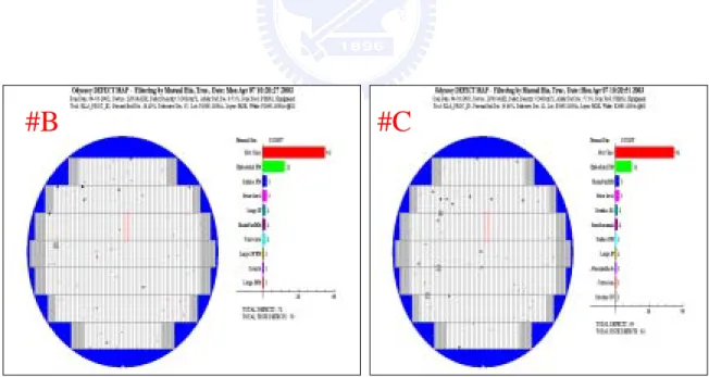
The film structure was formed by Al-Cu metal line and did post clean by dSP. All of wafers had been placed in boxes exceed 12 hours. Figure 2.6 shows “wafer A – just metal etch and didn’t asher”, the KLA map appeared metal corrosion on All wafer. This type corrosion metal was composed of chlorine, oxygen and aluminum; also inspected by SEM (second electron microscope). Figure 2.7 Shows the KLA maps of “wafer B – wafer held with cassette in open area” and “wafer C – wafer held with cassette in clean box”. Didn’t find corrosion metal on all wafers. Fig 2.8 shows “wafer D – wafer held with cassette in contaminated
fluoride box”, the KLA map appeared metal corrosion on top/bottom of wafer. This type corrosion metal was composed of fluorine, oxygen and aluminum; also inspected by SEM (second electron microscope).
What kinds of gas decomposition products caused metal corrosion? I planned another experiment to identify it. In IC’s manufacturing, have many different etchers and gas chemistry for special purpose; for example, poly etching with SF6/NF3 and oxide etching with
CHFx/CxFx. The experiment were putting wafers into different boxes that contaminated with different fluorine residues.
Wafer E – box be contaminated with high density plasma ploy etcher with SF6 gas.
Wafer F – box be contaminated with high density plasma poly etcher with NF3 gas.
Wafer G – box be contaminated with median density plasma poly etcher with NF3 gas
Wafer H – box be contaminated with high density plasma oxide etcher with C4F8 gas
Wafer I -- box be contaminated with median density plasma oxide etcher with C4F8 gas
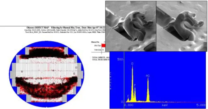
All of wafers had been placed in boxes exceed 12 hours. There were different corrosion results with different conditions. Figure 2.9 shows Wafer E – box be contaminated with high density plasma poly etcher with SF6 gas, there were serious metal corrosion on wafer.
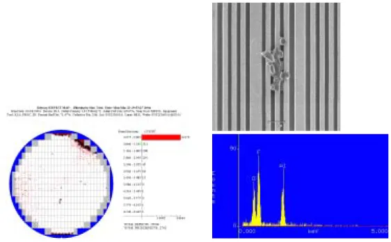
Inspected by SEM and composed of aluminum, oxygen, fluorine by EDX. Figure 2.10 shows Wafer F – box be contaminated with high density plasma poly etcher with NF3 gas, there were
metal corrosion on wafer. Inspected by SEM and composed of aluminum, oxygen, fluorine by EDX. The KLA map of wafer F was slighter than wafer E. Figure 2.11 shows wafer maps of wafer G – box be contaminated with median density plasma poly etcher with NF3 gas, wafer
H – box be contaminated with high density plasma oxide etcher with C4F8 gas and wafer I --
find any corrosion on three types of boxes.
2.3 Analysis
From experiments of above, characteristics of metal corrosion was summarized:
(a) This type metal corrosion does not come from the period of metal etching to post clean. It is known; the most metal corrosion come from metal etching process, photo resist strip process, post ACT-935 or dSP-HF clean process. According experiments of above, all evidences of metal corrosion don’t correlate with tools, chamber condition, parts lifetime, process margin, Fab environment, post clean problem and so on.
(b) The corrosion metal was composed of aluminum, oxygen and fluorine by EDX; but wasn’t composed of chlorine. Reviewing metal etching process, process gas only including Cl2 and BCl3 for reaction. It didn’t find any fluoride chemistry; like as SF6, CF4,
NF3, C4F8 and so on.
(c) The serious corrosion metal appears in environment of box that be contaminated with high density plasma ploy etcher with SF6 gas. The contaminated NF3 box only appears slight
corrosion metal. The other fluoride plasma, like as C4F8 and CF4, can’t find any corrosion
metal on wafer from experiments of above. Many of chemistries were used to play a role of reaction on different film. In current etching technology; SF6/HBr/Cl2/NF3 for poly
etching, C4F8/CH2F2 for oxide etching and BCl3/Cl2 for metal etching.
Therefore, the by-product of SF6 high density plasma is our candidate for contaminated
source of metal corrosion. In our Fab, metal etchers and poly etchers were located on the same line and used to carry cassettes with same boxes. So, the by-product of SF6 high density
plasma was absorbed on wafer in poly etcher and contaminated the carried boxes. When concentration of SF6 plasma by-product exceeds some limitation, attacking metal film with
moisture and appearing corrosion metal.
The contamination of fluorine come from DPS poly etcher, figure 3.2 shows wafer structure, the isotropic etching to define poly silicon depth on this step. The plasma chemistry contacts poly silicon film and nitride film at the same time, but only removes poly silicon film and keeps depth to target. The SF6 is popular gas to etch poly silicon with isotropic etch in
DPS poly etcher. The recipe is:
First step – Break-through CF4/source power/bias power for remove native oxide 4 sec
Second step – Main etch SF6/high density plasma of DPS chamber
The main reactions in high density plasma are dissociation/ionization of SF6 and reaction
with silicon. Electron impact dissociation/ionization:[8,9,10]
e- + SF6 Æ SFx + (6-x)F + e- x=0…5 (2.1)
e- + SF6 Æ SFx* + (6-x)F + 2e- x=0…5 (2.2)
Dissociative attachment:
e- + SF6 Æ SFx- + (6-x)F x=5,6 (2.3)
e- + SF6 Æ SF5 + F- (2.4)
Reaction with silicon:
4F + Si Æ SiF4 (2.5)
Decomposition of SF6 will be absorbed on wafer surface or out-diffusion from chamber to
loadlock, and then carried to box when wafers transport. The reactions with moisture contaminants are:[11]
SF4 + H2O Æ SOF2 + 2HF (2.6)
SF5 + OH Æ SOF4 + HF (2.7)
SOF4 + H2O Æ SO2F2 + 2HF (2.8)
SF5 + SF5 Æ S2F10 (2.9)
2SF5 + O2 Æ S2O2F10 (2.10)
HF is easy reaction with metal in room temperature:
6HF + 2Al Æ AlF3 + 3H2 (2.11)
AlF3 has very low volatility. Under normal etch conditions, ~100 mTorr, <60℃ , AlF3 is a
solid. This can be proven by figure 2.5 shows the corrosion wasn’t eliminated after metal etching back again. In order to confirm that HF is existence on box, the litmus test is a must. Preparing contaminated box with decomposition of SF6 and injecting a little water, the color
of litmus paper was changed and showed the water is acid.
2.4 Conclusion
The root cause of corrosion Al-Cu film happened irregularly was found, decomposition of SF6 in DPS poly etcher was the key. In order to eliminate corrosion metal, it is necessary to
setup a new production rule. Figure 2.12 shows two kinds of boxes for metal layers and non-metal layers, dedicated metal boxes can avoid contamination by decomposition of fluoride.
Since the dedicated metal boxes was implemented in mass production, have never seen corrosion metal that contaminated by fluorine. It is important to solve corrosion problem, because corrosion with fluorine have appeared in our Fabrication for several years. Not only get more up-time of tools, but also improve quality of product.
In the future, Boxless Fabrication is final goal. Next chapter, we also discuss about contamination of SF6 decomposition in an environment of box. Wafer transport by SMIF is
Chapter 3
Contamination of SF
6Plasma Decomposition in DPS Poly Etcher
3.1 Introduction of DPS Poly Etcher
In this chapter, we introduce the contamination of SF6 plasma decomposition in DPS
poly etcher. In IC’s manufacturing, the contamination of SF6 decomposition products
produces particle on wafer and suffers yield loss. Before start to read this chapter, it is necessary to understand “what is the DPS poly etcher”. The DPS chamber design allows independent control of ion-acceleration energy and plasma density to the wafer, yielding superior processing options. This is accomplished by adding an inductive RF subsystem over the ceramic dome to produce and sustain the plasma.
The bias RF (13.56MHz) power, applied to the cathode, determines the ion-acceleration energy. The source RF (12.56MHz) power, inductively coupled to the plasma through the ceramic dome, determines the plasma density.
Source RF current through the RF coil produces an alternating electromagnetic field that penetrates (through the dome) into the plasma, inducing RF electric fields which ionize and sustain the plasma. The induced electric fields do not produce the large sheath voltages associated with a capacitive reactor. Therefore, the source RF predominately influences plasma density. Bias RF (cathode) power is not significant in determining plasma density. Most of the bias RF power, which is typical one tenth of source RF power, is used in accelerating etchant ions to the wafer.
The source and bias RF subsystems are summarized as follows:
maximum out of 500 Watts. Its impedance-matching circuit “Bias Match” is mounted on the facilities box under the lower chamber.
(b) The source RF controls plasma density using a 12.56 MHz RF generator with a maximum output of 2000 Watts. Its impedance-matching circuit “Source Match” is located in the top section of the dome temperature control unit (DTCU). The DPS R1 uses a match with two adjustable capacitors.
3.2 The Problem and Experiment
The contamination of SF6 decomposition products produces particle on wafer and suffers
yield loss. At the first, it is necessary to know wafer structure and plasma etching condition. Figure 3.2 shows wafer structure, the isotropic etching to define poly silicon depth on this step. The plasma chemistry contacts poly silicon film and nitride film at the same time, but only removes poly silicon film and keeps depth to target. The SF6 is popular gas to etch poly
silicon with isotropic etch in DPS poly etcher. The recipe has two steps:
First step – Break-through CF4/source power/bias power for remove native oxide on top
of poly film
Second step – Main etch SF6/Low source power for depth control.
Figure 3.3 in this step, appeared semi-translucent hexagonal defects on the wafer by KLA inspected. If put the high level defect wafer in cassette box for 2, 24, 48 hours; the defect level is still high on the wafer. But take the high level defect wafer out cassette box for 2 hours, the defect level is down to half quickly. Therefore, the part of semi-translucent hexagonal defect is volatile in air sometime and remains in box. We have tried to remove they with popular clean skills, can reduce defect counts but can’t remove completely.
(a) SPM and APM clean: “SPM” means sulfuric acid (H2SO4) and (H2O2) on ratio 7:1.
“APM” means ammonia (NH4OH) and (H2O2) on ratio 1:4. SPM used to dehydrate
the organic particle (like photo-resist) and APM used to remove particle on silicon or oxide surface. Figure 3.4 shows the efficiency of SPM and APM. The left lot – defect counts reduce from 1253 to 25 at the 1st time clean. The right lot – defect counts reduce from 21762 to 300 at the 1st time clean and to 21 at the 2nd time clean. Figure 3.5 shows another experiment.
(b) Correlation between defect and chamber condition: One, chamber idle time test – chamber run intermittent for different idle time, the performance didn’t improve. Two, checking defect level before and after preventive maintenance (wet clean) – the defect level didn’t change at all. Three, implementing wafer season between production – using bare silicon wafer season between every wafer production, defect level was still high. Four, defect v.s. cbamber parts – checking the usage of chamber parts; liked ceramic dome, focus ring, gas distribution plate (GDP); still wasn’t any correlation.
(c) Couldn’t see hexagonal defect on daily particle monitor wafers. In order to monitor particle level of chamber, it is known to test oxide wafer by production recipe in IC’s manufacturing. From daily defect monitor data, couldn’t see hexagonal defect on daily particle monitor wafers.
(d) Comparison poly etching by different recipes on DPS chambers, the serious semi-translucent hexagonal defect most appeared on low source power recipe. The high source power or Ar gas injected recipe only appeared little hexagonal defect, the most of time couldn’t see any hexagonal defect on wafers; even film structures were
same.
(e) Add N2 plasma treatment in the end of poly etching: Figure 3.6 shows the result of
adding N2 plasma treatment in the end of poly etching. The semi-translucent
hexagonal defects still remain on wafer.
(f) Add O2 plasma treatment in the end of poly etching:
5mT/50 O2/150W/5 sec
Figure 3.7 shows the result of adding O2 plasma treatment in the end of poly etching.
The removed efficiency is good in treatment of 5, 10, 15 seconds. Therefore, the O2
plasma may be a best solution; using O2 plasma treatment can remove over ninety-nine
percent defect. Another question must be considered, did it influence poly etching when implement the O2 plasma treatment? Figure 3.8 shows the O2 plasma treatment didn’t
influence poly etching performance, the depth control stable in different treatment time. The etch rate of poly etching is same in different treatment time.
3.3 Analysis
From experiments of above, characteristics of semi-translucent hexagonal defects were summarized:
(a) Random small and volatile defect was observed after recess process. Semi-translucent hexagonal defects can’t volatilize in environment of box, but volatilize in open area. Defect level is decreasing during idling. Possible volatile compounds need to be high boil point.
(c) Volatile defect can’t come from chamber parts, such as chamber wall, gas distribution plate (GDP), focus ring and byproduct to be deposited on parts. Because semi-translucent defect appeared didn’t correlate with chamber idle time, PM cycle, changing time of parts and chamber condition during production. Chamber condition was changed after seasoning during production.
(d) Compound of semi-translucent hexagonal defect needs nitrogen source to react with SF6, which may explain why we never saw volatile particle on oxide particle monitor
wafer.
(e) From experiment “d”, semi-translucent hexagonal defect may form by radicals or species of low decomposition rate of SF6. The high source power or Ar gas injected
can induce SF6 to decompose smaller radicals or species.
Summarizing all analyses of above, preferring to say the “F11NS2” (or (F5S)2NF) is
the most possible compound in the volatile residue. The reason for the assumption were: (a) “F11NS2” is a stable compound, which may form from dissociated SF6 gas in the
plasma. From equation 2.1 to 2.9 can summary as below:
SF6 + SF5* + N = (F5S)2NF (3.1)
That may explain why serious semi-translucent hexagonal defect most appeared on low source power recipe and only little hexagonal defect on high source power or Ar gas injected recipe.
(b) “F11NS2” needs nitrogen source to react with SF6 and SF5, that may explain why we
(c) From table 3.1 shows boil point of “F11NS2” is 51.6 ° C, that may explain
Semi-translucent hexagonal defects can’t volatilize in environment of box, but volatilize in open area. Defect level is decreasing during idling.
From table 3.1, two candidates can meet the requirement, “F11NS2” and “F2N2S3”
(d) The etch byproduct of SiN is the nitrogen source in our candidate compounds, because the slow SiN etch rate we should not expect the compound of high nitrogen ratio may form during process. The purpose of this process is control poly depth and not removed nitride, the selectivity of poly to nitride is over 100. So, “F2N2S3” and
“F4N4S4” are not good candidates.
3.4 Conclusion
The “F11NS2” (or (F5S)2NF) is the most possible compound of the volatile residue.
Semi-translucent hexagonal defect was formed on nitride wafer in DPS poly etcher with SF6
plasma. Adding O2 plasma treatment in the end of poly etching is the best solution to remove
particle. The “F11NS2” (or (F5S)2NF) is oxidized by oxygen radicals. Under SF6 plasma with
1% O2 addition there was a remarkable decrease of the S2F10, and increase of SO2F2 and SOF4,
and decrease of SOF2.
SF5 + O Æ SOF4 + F (3.2)
SF4 + O2 Æ SOF4 + O (3.3)
SF2 + O2 Æ SO2F2 or SOF2 + O (3.4)
SOF2 + O Æ SO2F2 (3.5)
experience of another recipe in DPS poly etcher, adding argon in plasma also can reduce semi-translucent hexagonal defect. Because excited state of argon can impact SF6 molecule
and produce small fractions of decomposition. Concentration of SF5 may lower than haven’t
Chapter 4
Conclusion and Suggestion for Future Work
In this thesis, we investigated the effects of SF6 decomposition products in DPS poly
etcher. The evaluation of the effects of SF6 decomposition induced corrosion metal in DPS
poly etcher was discussed in chapter 2. When transport boxes are contaminated with SF6
decomposition from DPS poly etcher will induce cross contamination and corrosion of metal. The evaluation of semi-translucent hexagonal defect from SF6 decomposition in DPS poly
etcher was discussed in chapter 3. Some important conclusion are summarized below:
(a) In this thesis, SF6 decomposition products come from same source, same recipes and
same tools of DPS poly etcher. The condition of SF6 plasma is low power, low
pressure, high density, only pure SF6 gas. From equation 2.1 to 2.4, the
decomposition includes more excited state of SF6, SF5 or SF4. In the other word, the
fractions of SF6 decomposition are large and dissociation rate is low because the
electron energy is in low level. If injecting argon into plasma, this phenomenon will decrease gradually because excited state of argon has very large energy to impact molecule of SF6.
(b) SF6 decomposition products contaminate the transport boxes and induce metal
corrosion. From equation 2.5 to 2.10, SF5 or SF4 absorb on the surface of box and
react with moisture. HF is existence on the boxes and attack metal film cause corrosion metal. That may explain why the corrosion metal appears irregularly, sometime and somewhere. In some Fabrication, corrosion metal has correlation with different season because different concentration of H2O in air.
(c) SF6 decomposition products react with nitride film in DPS poly etcher, cause
semi-translucent hexagonal defect on wafer surface. The “F11NS2” (or (F5S)2NF) is
the most possible compound of the volatile residue. From equation (2.9) and (3.1), that may prove SF6 decomposition is on the wafer and carried out into the boxes.
(d) Adding O2 plasma treatment can eliminate defect very successfully. That can reduce
concentration of SF5 or SF4 very efficiently.
In the end of this thesis, we try to discuss about the future of IC’s manufacturing. From this thesis, both of by-products and decomposition products in etching easy induce defect or cross contamination in unfriendly environment. How to improve it? There are some suggestions can be used:
(a) Both of by-products and decomposition products in etching can’t be carried out chamber. One, using some ramp down procedure or treatment by N2/O2 plasma can
remove most of by-products on surface of wafer. Two, keeping pressure of transfer chamber higher than process chamber can avoid by-products diffusing out chamber.
(b) Replace whole cassette loadlock with single wafer loadlock, can avoid cross contamination when whole cassette is in loadlock. Because transferring out wafer needs waiting all wafers process completed, it is easy to induce cross contamination in the waiting time. But in single wafer loadlock, the previous etching wafer put on cassette in open area outside the loalock.
(c) Don’t use boxes to carry wafers. Two advanced transfer system have be implemented to IC’s manufacturing. One, automatic transport by unmanned vehicle.
Wafer transfer between stocker and machine uses automatic vehicle (AGV), doesn’t use man to hand-carry. Two, SMIF (standard mechanical interface) is popular transfer system for IC’s manufacturing.
(d) It is necessary to control environment of fabrication very accurately. The concentration of H2O is very important parameter. Many of chemistry of by-product
have relation with moisture, can form particle on wafer and kill yield. The concentration of ammonia is another important parameter, may cause quality of photo mask changed and induce particle on photo mask.
Reference
[01] P.L. Pai, C.H. Ting, W.M. Lee, R. Kuroda, “Metal Corrosion in Wet Resist-Stripping Process” Interface ’89, KTI microelectronics Seminar.
[02] R.R. Rogers, S.R. Wilson, “Localized Corrosion of Aluminum – 1.5% Copper Thin Films Exposed to Photoresist Developing Solution”, J. Vac. Sci. Technol. A9(3) May/Jun 1992, P1616 –1621
[03] K.H. Baek, C.I. Kim, K.H. Kwon, T.H. Kim, “Passivation Role of Fluorine on the Anticorrosion of AlCu Films After Plasma Etching” J. Vac. Sci. Technol. A 16(3), May/Jun 1998
[04] S. Bothra, H. Sur, V.Liang, R. Annapragada and J. Patel “Corrosion of Tungsten due to plasma charging in a metal plasma etcher”, VLSI Technology, Inc. 1109, Mckay Dr, San Jose, CA 95035
[05] S. Kirk, T. Maw, “Corrosion Prevention in The Bond Pad Cleaning Process” EKC Technology, Inc.
[06] S. Thomas, H.M. Berg, “Micro-Corrosion of Al-Cu Bonding Pads”, Motorola, Inc., P.153 [07] S. Graham, “Corrosion Issues in Solvent Processing”, Semitool Application Note,
February 1996
[08] C. Beryer, H. Jenett, D. Klockow, “Influence of Reactive SFx Gases on Electrode
Surfaces After Electrical Discharges under SF6 Atomsphere” IEEE Transactions on
Dielectrics and Electrical Insulation, Vol.7 No. 2, April 2000
[09] M. Piemontesi, L. Niemeyer, “Surface Reactions of SF6 Decomposition Products”, IEEE
annual report – conference on electrical and dielectric phenomena, San Francisco October 20-23, 1996
[10] L. Niemeyer, F.Y. Chu, “SF6 and the Atmosphere” IEEE Transactions on Electrical
[11] R.J. Van Brunt, J.T. Herron, “Fundamental Processes of SF6 Decomposition and
Oxidation in Grow and Corona Discharges” IEEE Transactions on Electrical Insulation, Vol.25 No.1, February 1990
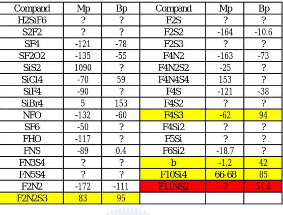
Compand Mp Bp Compand Mp Bp H2SiF6 ? ? F2S ? ? S2F2 ? ? F2S2 -164 -10.6 SF4 -121 -78 F2S3 ? ? SF2O2 -135 -55 F4N2 -163 -73 SiS2 1090 ? F4N2S2 -25 ? SiCl4 -70 59 F4N4S4 153 ? SiF4 -90 ? F4S -121 -38 SiBr4 5 153 F4S2 ? ? NFO -132 -60 F4S3 -62 94 SF6 -50 ? F4Si2 ? ? FHO -117 ? F5Si ? ? FNS -89 0.4 F6Si2 -18.7 ? FN3S4 ? ? b -1.2 42 FN5S4 ? ? F10Si4 66-68 85 F2N2 -172 -111 F11NS2 ? 51.6 F2N2S3 83 95
Table 3.1 Possible SF6 decomposition compounds during DPS poly etcher
Fig 2.1 Wafer map of metal corrosion inspected by KLA TENCOR tools, KLA map of slot 1,11,25 in whole cassette of 25 wafers
Slot 1
Slot 25 Slot 11
Fig 2.2 the pictures of corrosion metal, the top picture inspected by optical microscope (OM), the others inspected by second electron microscope (SEM)
LOT ID Corrosion Operation Date metal etch Alarm Post clean
lot 1 serious M2 E 0306 22:11 A-DPS NO dSP
lot 2 serious M2 E 0307 00:34 B-ECR NO ACT-935
lot 3 serious M3 E 0307 02:46 A-DPS NO ACT-935
lot 4 serious M2 E 0307 15:13 C-ECR NO ACT-935
lot 5 serious M3 E 0308 14:23 C-ECR NO ACT-935
lot 6 serious M3 E 0308 10:00 B-ECR NO dSP
lot 7 serious M2 E 0310 16:45 B-ECR NO ACT-935
LOT ID Corrosion Metal sputter Time PR coating Exposure Time
lot 1 serious C 0301 00:20 A C 0302 19:24 lot 2 serious B 0228 16:00 A B 0302 00:16 lot 3 serious A 0301 10:39 A A 0303 12:08 lot 4 serious C 0302 19:11 B C 0303 16:54 lot 5 serious C 0301 23:43 B C 0304 23:30 lot 6 serious A 0302 03:19 A B 0305 06:43 lot 7 serious B 0303 12:30 A B 0310 10:25
Fig 2.3 Corrosion metal appeared all kinds of metal etchers, post clean process, metal sputtering deposition, photoresist coater, photoresist exposure in all time.
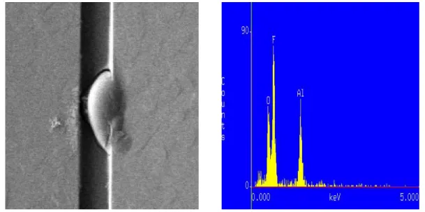
Fig 2.4 Corrosion metal was composed of aluminum, oxygen and fluorine by EDX
Fig 2.5 Corrosion metal wasn’t eliminated after metal etching back again
Al,TiN
Si,O
F,Al,O
Metal etching back again
Fig 2.6 Wafer A – just metal etched and didn’t asher, the KLA map appeared metal corrosion on All wafer. This type corrosion metal was composed of chlorine, oxygen and aluminum; also inspected by SEM (second electron microscope)
#B #C
Fig 2.7 The KLA maps of “wafer B – wafer held with cassette in open area” and “wafer C – wafer held with cassette in clean box”. Didn’t find corrosion metal on all wafers
Fig 2.8 Wafer D – wafer held with cassette in contaminated fluoride box, the KLA map appeared metal corrosion on top/bottom of wafer. This type corrosion metal was composed of fluorine, oxygen and aluminum; also inspected by SEM (second electron microscope)
Figure 2.9 Wafer E – box be contaminated with SF6 high density plasma of poly
etcher, there were serious metal corrosion on wafer. Inspected by SEM and composed of aluminum, oxygen, fluorine by EDX.
Figure 2.10 Wafer F – box be contaminated with NF3 high density plasma of poly
etcher, there were metal corrosion on wafer. Inspected by SEM and composed of aluminum, oxygen, fluorine by EDX.
Wafer I
Wafer G Wafer H
Figure 2.11 Wafer maps of wafer G – box be contaminated with NF3 median density
plasma of poly etcher, wafer H – box be contaminated with C4F8 high density
plasma of oxide etcher, wafer I -- box be contaminated with C4F8 median density
plasma of oxide etcher; we couldn’t find any corrosion on three types of boxes.
4/9 使用期
Metal 專用 Box 一般 Box
生一專用
M1.M2.M3 Etch
白底紅
Fig 2.12 In order to avoid contamination of metal, dedicated special boxes for metal wafer transport is a must.
Fig 3.2 wafer structure, isotropic dry etching to define poly 2 depth at this step.
P2
P1
Particle nitride Poly si oxide Fig 3.1 DPS poly etcher chamberFig 3.4 The efficiency of particle reduction with SPM + APM. The left lot – defect counts reduce from 1253 to 25 at 1st time clean. The right lot – defect counts reduce from 21762 to 300 at the 1st time and to 21 at the 2nd time clean.
After RRV
After RRV
Fig 3.7 The result of adding O2 plasma treatment in the end of poly etching. The
removed efficiency is good for treatment 5, 10, 15 seconds.
O2 plasma treatment 15 sec
O2 plasma treatment 10 sec
O2 plasma treatment 5 sec
No O2 plasma treatment
RC3 Depth
200
250
300
350
POR
5SEC
10SEC
15SEC
Fig 3.8 The O2 plasma treatment don’t influence poly etching