An ARROW-B Surface Plasmon Resonance Sensor in Aqueous
Environment
Ching-Hung Cheng and Yang-Tung Huang
Department of Electronics Engineering and Institute of Electronics National Chiao Tung University
1001 Ta-Hsueh Road, Hsinchu, Taiwan, Republic of China TEL: 03-5712121 Ext. 54138, FAX: 03-5724361
E-Mail: [email protected]
Abstract
An ARROW-B (antiresonant reflecting optical waveguide, type B) surface plasmon resonance (SPR) sensor operating in aqueous environment is proposed. The characteristics and optimization of the Au-coated ARROW-B SPR sensor with a buffer layer made of Cr inserted between Au and core are discussed. The detectable changes of the refractive index down to the order of 10−5can be achieved. The tolerances of the thickness and index changes of the first cladding layer, the second cladding layer, and the core layer are also discussed.
NSC project code: NSC90-2215-E009-024
Key Words: Waveguide sensors, surface plasmon resonance, antiresonant reflecting optical waveguides.
1
Introduction
Surface plasmon resonance for use in chemical and biochemical sensing has been receiving growing re-search efforts for the past two decades. Among several SPR sensor configurations, waveguide SPR sensors have many attractive features such as compact size, ruggedness, prospect of fabrication of mul-tiple/multichannel sensors on a single chip [1], [2]. In contrast to conventional waveguides, antiresonant reflecting optical waveguides (ARROW’s) utilizing antiresonant reflection as guiding mechanism instead of total internal reflection can perform low-loss single mode propagation with relatively large core size. Moreover, to support surface plasmon waves which are TM-polarized, polarization-insensitive ARROW-B [3] was adopted as the wave-guiding structure.
In this study, characteristics and design of ARROW-B SPR sensors have been investigated. A
dielectric overlay added onto the metal layer can be used to shift the operating range into the desired environment. Furthermore, an adhesion buffer layer of Cr is added between ARROW-B structure and the Au layer to enhance adhesion of Au layer to the dielectric material. A design example and the optimization of Au-coated ARROW-B SPR sensors are also presented.
2
Characteristics and Design of Au-coated ARROW-B SPR
Sensors
The basic structure of an ARROW-B SPR sensor shown in Fig. 1 consists of three sections. Sections
F1 and F2 are the input and output effective single-mode ARROW-B waveguides, and S is the sensing
section which supports surface plasmon waves. On top of the waveguide core is a layer of gold thin film. The length of the sensing region is assumed to be 2 mm.
When there is a variation in the refractive index of the environment (superstrate), the field profile of quasi-guided mode will change, and the output power through the sensor will be different. The relative output power through the ARROW-B SPR sensor can be expressed as:
p(L) = |a0(L)/a0(0)|2, (1)
S L = 2 mm x z n a Au n c = 1.460 n 2 = 1.460 n s = 3.500 d c = 4 µ m d 2 = 2 µ m d 1 = 0.27 µ m n 1 = 1.378 F 1 F 2 n a
Figure 1: Basic structure of an ARROW-B SPR sensor.
where a0(0) and a0(L) are the complex amplitudes of the fundamental modes at the input and output of
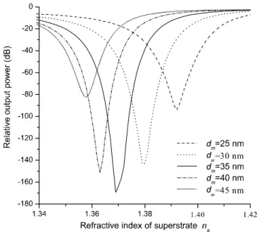
the sensor, respectively. Fig. 2 shows the relative output powers versus superstrate index nafor different
thickness of gold layer dm. The minimum relative output powers corresponds to the best resonant
coupling between the surface plasmon mode and the fundamental mode of the waveguide. Since the sensitivity of the sensor is proportional to the slope of the relative output power curve, the one which has a steeper slope is more suitable for sensing. By further comparison (not shown), we found that the
curve for dm= 35 nm has the steepest slope on both sides of the valley [4]. As a result, the thickness of
the gold layer of the following ARROW-B SPR sensors was set to be 35 nm.
Figure 2: Dependence of the relative output power on the superstrate index.
3
Au-coated ARROW-B SPR Sensors with a Cr Buffer layer
The structure of an ARROW-B SPR sensor with a buffer layer shown in Fig. 3. On top of the waveguide core is an additional buffer layer between gold and core in the sensing section S. The length of the sensing region is still assumed to be 2 mm. After adding an ultra-thin Cr layer, the real parts of the effective refractive indices are nearly the same.
L= 2 m m Au nc= 1.46 n2= 1.46 ns=3.5 dc= 4 µm d2=2 µm d1= 0.27 µm n1= 1.378 overlay dm= 35 n m εm= -12.2 -1.3i F1 S FF2 na ncr=3.49-4.36 i nf= 1.65 na na Cr
Figure 3: Structure of an ARROW-B SPR sensor with an adhesion layer.
4
Overlay Tuning and Optimization
Although the ARROW-B SPR sensor presented in the previous section is highly sensitive to superstrate index changes, the operating range is somewhat away from the desired aqueous environment. In order to shift the location of the minimum relative output power, a dielectric overlay was added on the top of the Au-coated ARROW-B SPR sensor as shown in Fig. 3.
To optimize the Au-coated ARROW-B SPR sensor in aqueous environment, the sensing resolution
or minimum detectable change in the superstrate index nadefined as (2) could be used as a measure [5]:
|δnmin| = ¯ ¯¯ ¯ ¯ M p(L) ∂ p(L) ∂ n ¯ ¯¯ ¯ ¯ n=na , (2)
where p(L) is the relative output power defined as (1), and M is the measurement precision of p(L) as
a percentage (typically, 1% [2]). A smaller | δnmin| value stands for a better resolution. To transform
δnmin into (δnmin)−1 is convenient for observation.
Table 1: The values of (δnmin)−1at na= 1.332 of Cr thicknesses ranging from 1 to 4 nm combined with
overlay thicknesses ranging from 11 — 16 nm.
Cr (nm) \ overlay (nm) 11 12 13 14 15 16
1 10593 12589 6481 -5629 -15570
2 11399 14358 -3488 -17008 -13372
3 10234 12213 11623 -27031 -14264
4 10669 12498 -3504 -14956 -12317
Table 4-1 lists the values of (δnmin)−1 at na = 1.332 for each combination of Cr-thickness and
overlay-thickness. When dcr = 3 nm and df = 14 nm, the value of | (δnmin)−1| which equals to 27031
is the largest among all. As a result, dcr = 3 nm and df = 14 nm is best condition for the ARROW-B
SPR sensor having the resolution of δnmin= −3.7 × 10⁻⁵.
5
Influence of Device Parameter Variation on the Performance
of the SPR Sensor
To study the tolerance of the sensor, the resolution δnmin is examined with respect to the thickness and
refractive index of the first cladding layer (d1 and n1), the second cladding layer (d2 and n2), and the
Figure 4: The dependence of δnmin on the core thickness dc.
at optimal condition. The ranges of each layer are
0.270 − 0.270 × 10% < d1< 0.270 + 0.270 × 10% −→ 0.243 < d1< 0.297 (µm),
2.000 − 2.000 × 10% < d2< 2.000 + 2.000 × 10% −→ 1.800 < d2< 2.200 (µm),
4.000 − 4.000 × 10% < dc< 4.000 + 4.000 × 10% −→ 3.600 < dc < 4.400 (µm).
In the first interval, δnminchanges very little, and the worst value is about −4.6×10⁻⁵, the resolution
is still very good and the tolerance of our sensor to the first cladding thickness is good. In the second
interval, it has a worst value of about −5.7 × 10⁻⁵, the tolerance to the second cladding thickness is
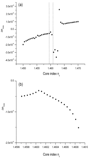
also good. As for the case of the core thickness change shown in 4, when the core thickness is less than
3.7 µm, the resolution is out of the order of 10−5. Although the thickness of and the core affects the
resolution more seriously than those of the first cladding layer and the second cladding layer do, this won’t be a big problem because the I.C. technology at present is so good that the thicknesses can be controlled very precisely.
Next consider the changes of δnmin with respect to the index variation of the three layers. The
variation of the refractive index in each case is set as a value of ±0.01. The tolerance of the device to
the first cladding index is very good because | δnmin| is less than 5.0 × 10⁻⁵ during the whole interval.
If the second cladding index is larger than 1.463, the resolution will be out of the order of 10−5.As
shown in Fig. 5(a), it can be seen that the resolution is strongly influenced by the refractive index of the core. Assume that the material of the core is very pure and the variation of the refractive index is
caused by the temperature change. The refractive index change per Celsius (dn/dT ) of the core (SiO2)
is 11.9 × 10⁻⁶/◦C, and nc is equal to 1.46 at 25◦C [6]. If the temperature of the aqueous environment
ranges from 0◦C (freezing point) to 100◦C (boiling point), the range of refractive index of SiO
2 will be
1.45971 to 1.46087. Fig. 5(b) is a plot of δnmin versus nc of the above range. When δnmin falls beyond
the order of 10−5, n
c is about 1.46071 which corresponds to 86◦C. If the operating temperature is lower
than 86◦C, the resolution will be better than 10 × 10−5.
6
Conclusion
An Au-coated ARROW-B SPR sensor operating in aqueous environment has been investigated. An ARROW-B SPR sensor with an adhesion buffer layer of Cr is more stable. This new layer is so thin
that the characteristics of SPW hardly change. Even when dcr= 3 nm and df = 14 nm, the resolution
Figure 5: The dependence of δnmin on the core index nc (a) from 1.450 to 1.470 (b) from 1.45971 to
5.56 ×10⁻⁵[4]. The ARROW-B SPR sensor is still competitive to conventional waveguide sensors having
resolution ∼ 6 × 10⁻⁵ [7].
The tolerances to the first and second cladding thicknesses and to the first cladding index are good whereas those to the core thickness and to the second cladding index are acceptable as long as the core thickness is not lower than 3.7µm or the second cladding index is not larger than 1.463. As for the core index change which affects the resolution most seriously among all, the resolution will still be better
than 10 × 10−5 if the core index is lower than 1.46071. When the operating temperature is less than
86◦C in the aqueous environment with the resolution better than 10 × 10−5.
References
[1] R. D. Harris and J. S. Wilkinson, “Waveguide surface plasmon resonance sensors,” Sensors and Actuators B, vol. 29, pp. 261—267, 1995.
[2] J. Homola, J. Ctyroky, M. Skalsky, J. Hradilova, and P. Kolarova, “A surface plasmon resonance based integrated optical sensor,” Sensors and Actuators B, vol. 38—39, pp. 286—290, 1997.
[3] T. Baba and Y. Kokubun, “New polarization-insensitive antiresonant reflecting optical waveguide (ARROW—B),” IEEE Photon. Technol. Lett., vol. 1, no. 8, pp. 232—234, 1989.
[4] W. Z. Chang, “Investigation on ARROW-B SPR Sensors in Aqueous Environment, ”Master Thesis, Institute of Electronics, National Chiao Tung University, 2001.
[5] M. N. Weiss, R. Srivastava, H. Groger, P. Lo, and S. F. Luo, “A theoretical investigation of environ-mental monitoring using surface plasmon resonance waveguide sensors,” Sensors and Actuators A, vol. 51, pp. 211—217, 1996.
[6] Crystran Ltd, http://www.crystran.co.uk/.
[7] J. Ctyroky, J. Homola, and M. Skalsky, “Tuning of spectral operation range of a waveguide surface plasmon resonance sensor,” Electron. Lett., vol. 33, pp. 1246—1248, 1997.