68 IEEE ELECTRON DEVICE LETTERS, VOL. 28, NO. 1, JANUARY 2007
Bond Pad Design With Low Capacitance in CMOS
Technology for RF Applications
Yuan-Wen Hsiao, Student Member, IEEE, and Ming-Dou Ker, Senior Member, IEEE
Abstract—A new bond pad structure in CMOS technology with low capacitance for gigahertz radio frequency applications is proposed. Three kinds of inductors stacked under the pad are used in the proposed bond pad structure. Experimental results have verified that the bond pad capacitance is reduced due to the cancellation effect provided by the inductor embedded in the proposed bond pad structure. The new proposed bond pad structure is fully process-compatible to general CMOS processes without any extra process modification.
Index Terms—Bond pad, capacitance, loss, radio frequency integrated circuit (RF IC).
I. INTRODUCTION
W
ITH THE advantages of high integration capability and low cost for mass production, radio frequency inte-grated circuits (RF ICs) operating in gigahertz frequency bands have been implemented in CMOS technology. However, the undesired parasitic capacitances at the input pads of silicon chips often limit the high-frequency performance of RF ICs. The bond pad capacitance should be minimized to mitigate the RF performance degradation. Moreover, on-chip electrostatic discharge (ESD) protection devices are also placed around the input pad, which further decrease the design budget because of the extra parasitic capacitance from the ESD protection devices [1]–[4]. The parasitic capacitance resulted from the bond pad metal, and the overlapped substrate was not reduced with the progress of CMOS technology. In some CMOS integrated RF front ends, the bond pad capacitance can be incorporated as a part of the matching network. Recently, several techniques were reported to reduce the bond pad capacitance [5]–[7]. A bond-pad structure realized with special layout patterns, which have smaller metal area and additional diffusion layers, had been demonstrated with smaller bond pad capacitance [5]. An-other bond pad using depletion-insulation structure to improve crosstalk isolation and Q-factor had been presented [6]. Be-sides, a bond pad structure realized with semi-insulating porous silicon had also been reported to reduce the bond pad capacitance [7].In this letter, a new bond pad structure with embedded inductor is proposed to reduce the bond pad capacitance. The
Manuscript received August 1, 2006; revised October 19, 2006. This work was supported in part by the National Science Council (NSC), Taiwan, R.O.C., under Contract NSC 95-2221-E-009-290, and in part by the Faraday Technol-ogy Corporation, Taiwan, R.O.C. The review of this letter was arranged by Editor S. Kawamura.
The authors are with the Nanoelectronics and Gigascale Systems Laboratory, Institute of Electronics, National Chiao-Tung University, Hsinchu, Taiwan, R.O.C. (e-mail: [email protected]).
Digital Object Identifier 10.1109/LED.2006.887631
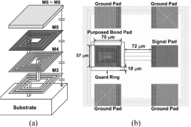
Fig. 1. (a) Proposed bond pad structure with an embedded three-layer stacked inductor in a 0.13-µm 1P8M CMOS process. (b) Layout top view of the test pattern to measure the bond pad capacitance.
proposed bond pad structure possesses several features. First, it is compatible to standard CMOS process without extra process modification. Second, the proposed bond pad has the same dimensions as that of the reference bond pad to maintain good bonding reliability. Third, the proposed bond pad has low parasitic capacitance, which is suitable for high-frequency applications.
II. PROPOSEDBONDPADSTRUCTURES
A 0.13-µm 1P8M CMOS process is used in this letter, and the typical bond pad provided by foundry is fully implemented with eight metal layers (from metal 1 to metal 8). However, the parasitic capacitance of the bottom metal layer (metal 1) and the overlapped substrate is too large for RF applications. In order to reduce the parasitic capacitance, the lower metal layers are removed in the bond pads. However, using only the top metal layer to implement the bond pads has some concerns on bond-ing reliability. To compromise the dilemma between parasitic capacitance and bonding reliability, the reference bond pad used in this letter is realized with only top three metal layers, which are metals 8, 7, and 6 in a 0.13-µm CMOS process.
The proposed bond pad structure with an embedded induc-tor is illustrated in Fig. 1(a), where a stacked inducinduc-tor [8] implemented with three metal layers (metals 5, 4, and 3) is embedded under the reference bond pad. Since the inductor is implemented within the region of the bond pad, the proposed bond pad occupies the same area as the reference one. The bond pads with three kinds of inductors, which are one-layer inductor (implemented with metal 5), three-layer stacked inductor
HSIAO AND KER: BOND PAD DESIGN WITH LOW CAPACITANCE IN CMOS TECHNOLOGY FOR RF APPLICATIONS 69
Fig. 2. Extracted bond pad capacitances among the fabricated bond pads under different frequencies.
Fig. 3. Measured losses among the fabricated bond pads under different frequencies.
(implemented with metals 5, 4, and 3), and five-layer stacked inductor (implemented with metals 5, 4, 3, 2, and 1), have been designed in the experimental test chip for comparison. The inductors are drawn with the track width of 4µm, track spacing of 1 µm, and five turns. The inductor designed in such architecture is used to increase the inductance under the prespecified region to cancel the bond pad capacitance.
Fig. 1(b) shows the layout top view of the test patterns used to measure the bond pad capacitance. Ground–signal–ground (G–S–G) pads are adopted to facilitate on-wafer measurement. The proposed bond pad occupies the same area(70 × 57 µm) as that of the reference bond pad. A guard ring is implemented to encircle the proposed bond pad. With the guard ring con-nected to the substrate, the parasitic capacitance between the bond pad and the substrate can be characterized.
III. EXPERIMENTALRESULTS ANDDISCUSSION
The proposed bond pads with one-, three-, and five-layer stacked inductors as well as the reference bond pad have been fabricated in the same silicon chip in a 0.13-µm 1P8M CMOS process. The two-portS-parameters of the fabricated bond pads
Fig. 4. Circuit model of the proposed bond pad.
were characterized by on-wafer measurement with Cascade Air Coplanar G–S–G microwave probes and the Agilent 8510C network analyzer. The measured frequency range was from 3 to 10 GHz.
The Z-parameters can be obtained from the conversions between two-port S-parameters and Z-parameters [9]. Then, the bond pad capacitance (Cpad) was extracted as Cpad=
−1/(ωIm(Z11)), where Z11is the impedance seen from port 1 with port 2 open. Fig. 2 shows the extracted bond pad ca-pacitances among the fabricated bond pads under different frequencies. As shown in Fig. 2, the reduction on the bond pad capacitance is more significant when a stacked inductor realized with more metal layers is embedded under the bond pad. With a five-layer stacked inductor in the proposed bond pad, the bond pad capacitance can be even reduced to almost 0 fF at a specific frequency band (4.3 ∼ 4.8 GHz). The bond pad capacitance is reduced due to the positive reactance contributed from the embedded inductor. For example, the bond pad capacitance of the proposed structure with one-, three-, and five-layer stacked inductors can be reduced 2.9%, 58.9%, and 49.3%, respectively, from the original value (the reference pad) at 6.5 GHz. With more sophisticated design on the embedded inductor, the fre-quency band in which the bond pad capacitance is reduced can be further extended.
The measured losses among the fabricated bond pads are shown in Fig. 3. In the loss measurement, port 1 and port 2 of the network analyzer were both connected to the top metal plate of the bond pad. The loss was obtained from the measured
S21 with the relation of Loss(dB) = −(S21(dB)). Since the impedance of the five-layer stacked inductor is much higher than that of the one-layer inductor, the proposed pad with five-layer stacked inductor has the least loss, while the proposed pad with one-layer inductor has the most loss among the three kinds of proposed pads. From 3 to 10 GHz, the proposed bond pad with five-layer stacked inductor has a loss less than 0.65 dB. Because the inductor was connected to the substrate in the proposed bond pad structure, the proposed bond pad has more loss as compared with the reference bond pad. However, since all I/O pads need to be accompanied with ESD protection circuits, the loss of the proposed bond pad will not be the critical part at the input or output nodes because of the larger signal loss caused by the on-chip ESD protection devices. The circuit model of the proposed bond pad is shown in Fig. 4.
70 IEEE ELECTRON DEVICE LETTERS, VOL. 28, NO. 1, JANUARY 2007
plates of the bond pad and the substrate.CC1,CC2,R1, andR2 represent the coupling between the metal plates and the stacked inductor.CF represents the parasitic capacitance between the metal layers in the stacked inductor.LS andRSare the induc-tance and series resisinduc-tance of the stacked inductor, respectively.
COX1andCOX2represent the capacitance between the stacked
inductor and the substrate. CSUB and RSUB represent the parasitic effects of the substrate.
At 5 GHz, the capacitance of the proposed bond pad with five-layer stacked inductor is only 3.15 fF, which is quite small. Therefore, the proposed bond pad is suitable for gigahertz applications. The frequency at which the capacitance of the proposed bond pad is minimum can be adjusted by changing the dimensions of the stacked inductor and the metal plates of the bond pad. To mitigate the impact of the bond pad loss, the proposed bond pad can be codesigned with on-chip ESD protection devices. For example, the impedance isolation tech-nique had been used to optimize the RF characteristics at the input and output nodes, which have the bond pad and ESD protection devices [10].
IV. CONCLUSION
By inserting a stacked inductor under a bond pad, the proposed bond pad performs low parasitic capacitance. The experimental results have proven that the embedded inductor can be used to reduce the bond pad capacitance. The proposed low-capacitance bond pad structure, achieved by layout modifi-cation, is fully process-compatible to general CMOS processes for RF applications.
ACKNOWLEDGMENT
The authors would like to thank W.-C. Wang for his valuable technical discussions. The authors would also like to thank the reviewers for their valuable suggestions to improve this letter.
REFERENCES
[1] C. Richier, P. Salome, G. Mabboux, I. Zaza, A. Juge, and P. Mortini, “Investigation on different ESD protection strategies devoted to 3.3 V RF applications (2 GHz) in a 0.18µm CMOS process,” in Proc. EOS/ESD
Symp., 2000, pp. 251–259.
[2] M.-D. Ker, T.-Y. Chen, C.-Y. Wu, and H.-H. Chang, “ESD protection design on analog pin with very low input capacitance for high-frequency or current-mode applications,” IEEE J. Solid-State Circuits, vol. 35, no. 8, pp. 1194–1199, Aug. 2000.
[3] M.-D. Ker, Y.-W. Hsiao, and B.-J. Kuo, “ESD protection design for 1- to 10-GHz distributed amplifier in CMOS technology,” IEEE Trans. Microw.
Theory Tech., vol. 53, no. 9, pp. 2672–2681, Sep. 2005.
[4] M.-D. Ker and C.-Y. Chang, “ESD protection design for CMOS RF inte-grated circuits using polysilicon diodes,” Microelectron. Reliab., vol. 42, no. 6, pp. 863–872, Jun. 2002.
[5] M.-D. Ker, H.-C. Jiang, and C.-Y. Chang, “Design on the low-capacitance bond pad for high-frequency I/O circuits in CMOS technology,” IEEE
Trans. Electron Devices, vol. 48, no. 12, pp. 2953–2956, Dec. 2001.
[6] S. Lam, P. K. T. Mok, P. K. Ko, and M. Chan, “High-isolation bonding pad design for silicon RFIC up to 20 GHz,” IEEE Electron Device Lett., vol. 24, no. 9, pp. 601–603, Sep. 2003.
[7] K. Chong and Y.-H. Xie, “Low capacitance and high isolation bond pad for high-frequency RFICs,” IEEE Electron Device Lett., vol. 26, no. 10, pp. 746–748, Oct. 2005.
[8] A. Zolfaghari, A. Chan, and B. Razavi, “Stacked inductors and transform-ers in CMOS technology,” IEEE J. Solid-State Circuits, vol. 36, no. 4, pp. 620–628, Apr. 2001.
[9] D. M. Pozar, Microwave Engineering, 2nd ed. New York: Wiley, 1998. [10] M.-D. Ker, C.-I. Chou, and C.-M. Lee, “A novel LC-tank ESD
protec-tion design for giga-Hz RF circuits,” in Proc. IEEE RFIC Symp., 2003, pp. 115–118.