超寬頻無線網路應用之互補金氧半高動態範圍可變增益放大器設計
84
0
0
全文
(2) 超寬頻無線網路應用之 互補金氧半高動態範圍可變增益放大器設計 A CMOS Wide Dynamic Variable Gain Amplifier Design for Ultra-Wideband Wireless Applications. 研 究 生: 宋兆鈞. Student:Chao-Chun Sung. 指導教授: 溫瓌岸 博士. Advisor:Dr. Kuei-Ann Wen Dr. Wen-Shen Wuen. 溫文燊 博士. 國 立 交 通 大 學 電子工程系 電子研究所碩士班 碩 士 論 文. A Thesis Submitted to the Institute of Electronics College of Electrical Engineering and Computer Science National Chiao Tung University In Partial Fulfillment of the Requirements For the Degree of Master of Science In Electronic Engineering. 中華民國九十四年六月 ii.
(3) 超寬頻無線網路應用之 互補金氧半高動態範圍可變增益放大器設計 學生:宋兆鈞. 指導教授:溫瓌岸 博士 溫文燊 博士. 國立交通大學電子工程系 電子研究所碩士班. 摘. 要. 本論文針對超寬頻(UWB)無線網路應用提出低功率高動態範圍可變增益放大器之設計。 本文提出之可變增益放大器 (VGA)採用高範圍的假指數電路架構,此架構分別提供單級 約 30dB 之可變動態範圍,在高動態範圍的架構下,以較少的串接級來達到所需的動態 範圍並以達成低功耗和寬頻之設計目標。將此可變增益放大器架構應用於超寬頻射頻前 端接收器,加上後級放大器,以符合高增益之要求,並且增加一組回授二階濾波器,以 補償電路不匹配之直流電壓偏移,進而有助於提升整體可變增益放大器之效能。經由 0.18-μm CMOS 製程進行電路實作,量測出 230MHz 的大頻寬與約 9.5~11.2mW 的低功耗, 同時具有 73dB 的最大功率增益、21.5dB 的最低增益值,並在 400mVpp 輸出電壓時得 40dB 全諧波失真,驗證此高動態範圍之可變增益放大器電路架構之優點。此超寬頻射頻前端 接收器參考多頻帶正交頻率多重分割技術規格草案的需求。. i.
(4) A CMOS High Dynamic Variable Gain Amplifier Design for Ultra-Wideband Wireless Applications. Student:Chao-Chun Sung. Advisors:Dr. Kuei-Ann Wen Dr. Wen-Shen Wuen. Department of Electronics Engineering Institute of Electronics National Chiao-Tung University. ABSTRACT. This thesis presents a low-power design of a CMOS high dynamic variable gain amplifier (VGA) for ultra-wideband (UWB) wireless applications. To achieve low power consumption and. wide. operating. bandwidth,. the. proposed. VGA. employing. a. wide-range. pseudo-exponential circuit topology is presented, which can provide about 30dB dynamic per-stage. With the proposed topology, the amplifier stages capable of achieving a required gain range can be reduced and the level of power consumption is tremendously lowered. The novel topology of low power UWB VGA is applied to the RF front-end design for the UWB direct conversion receiver. A wideband post amplifier is designed for the purpose of high gain. The DC offset voltage will be reduced by a feedback 2nd order low-pass filter and consequently help improving overall performance of the VGA. A circuit implementation in 0.18-µm CMOS process shows a 230MHz bandwidth. The amplifier provides a maximum. ii.
(5) forward gain of 73 dB while drawing 11.2 mW and a minimum forward gain of 21.5 dB while drawing 9.4 mW from a 1.8-V supply. The harmonic distortion is batter than 40dB under the output signal magnitude is 400m Vpp. In this thesis, design optimization for the variable gain amplifiers in wide bandwidth applications is also verified. The UWB receiver front-end referenced to the Multi-Band OFDM with operation frequency range 3-10 GHz demonstrates low power, high gain, and wide bandwidth.. iii.
(6) 誌. 謝. 在這碩士研究的兩年歲月,首先要感謝的是 TWT 實驗室的大家長─溫瓌岸教授,賦 予了大家豐富的資源和環境,溫文燊博士,給予精闢的教導並在研究上給予方向,在兩 位細心的指導下,完成了這篇碩士論文。另外,感謝各位口試委員們─陳巍仁教授、高 曜煌教授與詹益仁教授,提供寶貴的建議與指教。 感謝實驗室的學長姐們─周美芬學姊、彭嘉笙學長、陳哲生學長、張孟凡學長、莊 源欣學長、林立協學長及鄒文安學長等在研究上的幫助與意見,讓我獲益良多。 感謝實驗室的同學─健銘、皓名、相霖、富昌、格輝、昌慶,在課業和日常生活上, 大家總是相互的扶持幫助;在學業上的討論與切磋。也感謝實驗室的學弟們─俊憲、志 徳、振威、彥宏、懷仁、俊閔、彥凱、書瑋等,讓整個實驗室充滿了歡樂的氣息;另外, 感謝 301 室的助理─宜蕐、316 室的助理─苑佳、怡倩、淑怡,時常協助我們,感謝佳 毅在實驗室工作站的管理,使得我有一個好的模擬環境。 最後,感謝我的每一個親人,感謝父母親在整個求學生涯的幫助,總是大力的支持 我所做的決定,感謝我的大哥與大嫂在研究生活中給我些額外的支柱,感謝我的二哥與 未來的二嫂在我失戀的時候總是給我鼓勵與開導,感謝小弟對我的體諒,最後感謝高中 的死黨們在我人生最低潮時陪伴者我;大家在我的成長過程中,一路陪伴著我,鼓勵我, 向未來邁進。. 誌予. 2005. 宋兆鈞. iv.
(7) Contents 摘要. i. Abstract. ii. 致謝. iv. Contents. v. List of Figures. vii. List of Tables. x. Chapter 1 Introduction. 1. 1.1. Motivation .......................................................................................................... 2. 1.2. Organization ....................................................................................................... 3. Chapter 2 Basic Concepts in VGA Design. 4. 2.1. Basic VGA Topologies ....................................................................................... 4. 2.2. Constant Settling Time of AGC Loop ................................................................ 8. 2.3. Pseudo Exponential Technique......................................................................... 14. Chapter 3 Novel High Dynamic Range Technique. 17. 3.1. Conventional Approach .................................................................................... 17. 3.2. Proposed Approach........................................................................................... 19. 3.3. Comparison....................................................................................................... 22. 3.4. Deep Submicron Effect .................................................................................... 25. Chapter 4 Variable Gain Amplifier Design. 27. 4.1. MB-OFDM Proposal Brief............................................................................... 27. 4.2. Variable Gain Amplifier Architecture............................................................... 30. 4.3. Variable Gain Amplifier Circuit ....................................................................... 32. 4.4. Post Amplifier & Buffer ................................................................................... 36 v.
(8) 4.5. Offset Cancellation ........................................................................................... 40. 4.6. Digital control circuit ....................................................................................... 42. Chapter 5 Implementation and Experimental Results. 45. 5.1. Overall VGA Circuit Simulation ...................................................................... 45. 5.2. Chip Layout and Post-Layout Simulation ........................................................ 49. 5.3. ESD Protection and the Package Model........................................................... 51. 5.4. PCB Design ...................................................................................................... 52. 5.5. Testing Setup .................................................................................................... 54. 5.6. Measurement Results........................................................................................ 56. 5.7. Error Correction................................................................................................ 61. 5.8. Summary........................................................................................................... 65. Chapter 6 Conclusions. 67. 6.1. Summary.......................................................................................................... 67. 6.2. Recommendations for Future Work.................................................................. 68. Bibliography. 69. Publication List. 71. Vita. 72. vi.
(9) List of Figures Figure 1. The Multi-Band OFDM frequency band plan[1]. 1. Figure 2. The direct conversion architecture for UWB receiver. 2. Figure 3. Basic topologies for gain variation.. 5. Figure 4. Two stages providing variable gain.. 6. Figure 5. Block diagram of a front end circuit.. 8. Figure 6. Block diagram of an AGC circuit.. 9. Figure 7. Model of generalized AGC circuit.. 10. Figure 8. Pseudo exponential gain versus control parameter.. 15. Figure 9. Schematic of the conventional variable gain amplifier.[5]. 18. Figure 10 Conventional circuit approximation on a decibel scale.. 19. Figure 11 The concept of the proposed methodology. 20. Figure 12 Proposed technique.. 21. Figure 13 Proposed simulation on a decibel scale.. 22. Figure 14 Real term generated by inductively source degeneration.. 23. Figure 15 Transmitter power spectral density mask in MB OFDM proposal.. 28. Figure 16 System architecture of UWB transceiver.. 29. Figure 17 UWB receiver path.. 29. Figure 18 Variable gain amplifier architecture.. 30. Figure 19 Schematic of the variable gain amplifier.. 32. Figure 20 Common mode feedback amplifier.. 33. Figure 21 Signal stage VGA simulation.. 34. Figure 22 Stability simulation setup.. 35. Figure 23 Phase margin simulation (high gain).. 35. vii.
(10) Figure 24 Phase margin simulation (low gain).. 35. Figure 25 Schematic of the post amplifier.. 36. Figure 26 Frequency response of the post amplifier.. 37. Figure 27 Phase margin of the post amplifier.. 38. Figure 28 (a) Conventional source follower, (b) Super source follower circuit.. 38. Figure 29 Small signal mode of the super source follower.. 39. Figure 30 Simulation result of the output buffer with 10pF load.. 40. Figure 31 The gain cell in the feedback path.. 41. Figure 32 VGA input stage and offset substractor.. 42. Figure 33 Simulation result of the input stage and offset substractor.. 42. Figure 34 Linear load which is a back-to-back connect of current mirrors.. 43. Figure 35 A 6-bit current steering DAC.. 44. Figure 36 Dynamic gain range simulation result.. 46. Figure 37 Frequency response simulation result.. 46. Figure 38 Output swing simulation (Low gain).. 47. Figure 39 Output swing simulation (High gain).. 47. Figure 40 P1dB simulation (High gain & Low gain).. 48. Figure 41 Power consumption.. 48. Figure 42 Circuit layout of the voltage control VGA.. 50. Figure 43 Circuit layout of the Digital control VGA (packaged version).. 50. Figure 44 ESD protection circuit.. 51. Figure 45 Package Model.. 52. Figure 46 Package Model.. 52. Figure 47 The layout of the PCB.. 53. Figure 48 Testing setup.. 54. viii.
(11) Figure 49 Transformer.. 55. Figure 50 Device under test PCB with transformer.. 55. Figure 51 Device under test PCB without transformer.. 55. Figure 52 Measurement environment.. 56. Figure 53 Measurement result of the output swing.. 57. Figure 54 Measurement result of the harmonic distortion.. 57. Figure 55 Measurement result of the harmonic distortion.. 58. Figure 56 Measurement result of the gain versus control voltage.. 59. Figure 57 Measurement result of the gain error. (compared with simulation). 59. Figure 58 Measurement result of the gain error. (compare with ideal). 60. Figure 59 Measurement result for Digital control version.. 61. Figure 60 Comparison between simulation result and ideal function.. 62. Figure 61 Pseudo-exponential with gds effect by matlab.. 62. Figure 62 The VGA circuit after modified.. 63. Figure 63 The VGA simulation after modified (one stage).. 64. Figure 64 The improved VGA simulation gain error (one stage).. 64. Figure 65 The error comparison.. 65. ix.
(12) List of Tables Table 1.. Comparison between several VGA method. 16. Table 2.. Receiver performance requirement in MB OFDM proposal.. 28. Table 3.. A simple specification of UWB VGA circuit.. 31. Table 4.. Power consumption for Mode1 DEV(3-Band).. 31. Table 5.. The simulation results of UWB VGA circuit.. 48. Table 6.. Components of the PCB. 53. Table 7.. Measurement Summary. 66. Table 8.. Measurement Comparison. 66. x.
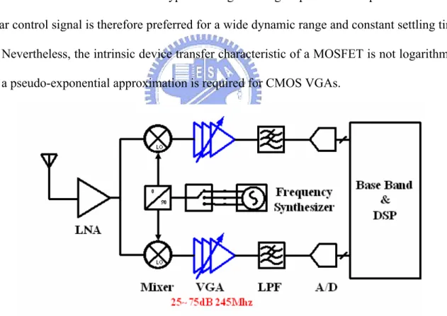
(13) Chapter 1 Introduction Recently, the Federal Communications Commission (FCC) in US approved the use of ultra-wideband (UWB) technology for commercial applications in the 3.1-10.6 GHz [1]. UWB performs excellently for short-range high-speed uses, such as automotive collision-detection systems, through-wall imaging systems, and high-speed indoor networking, and plays an increasingly important role in wireless personal area network (WPAN) applications. This technology will be potentially a necessity in our daily life, from wireless USB to wireless connection between DVD player and TV, and the expectable huge market attracts various industries. The IEEE 802.15.3a task group (TG3a) is currently developing a UWB standard from the proposals submitted by different companies. It is now left with two primary proposals, Multi-Band OFDM and Direct Sequence UWB. The newly unlicensed UWB opens doors to wireless high-speed communications and has been exciting tremendous academic research interest.. Figure 1. The Multi-Band OFDM frequency band plan[1] 1.
(14) 1.1. Motivation. Because the IEEE802.15.3a task group sets targets of low power consumption and low cost, complementary metal-oxide semiconductor (CMOS) process with the advantages of cost reduction and integration feasibility becomes the technology for trend to implement variable gain amplifier (VGA) implement. For this system, the VGA usually requires 3-dB bandwidth wider than 245 MHz and 50dB dynamic gain range in the receiver path [2]. The UWB receiver architecture is shown in Figure 2. The gain of a VGA should increase linearly on a decibel scale to linear control voltage to minimize the output voltage variation. The exponential transfer characteristic type VGA generating exponential output current for a linear control signal is therefore preferred for a wide dynamic range and constant settling time [3]. Nevertheless, the intrinsic device transfer characteristic of a MOSFET is not logarithmic, and a pseudo-exponential approximation is required for CMOS VGAs.. Figure 2. The direct conversion architecture for UWB receiver. There are some examples of developments of pseudo-exponential topologies to approximate its gain polynomial to exponential [4], [5]. The maximum gain range of the conventional topology has a 15 dB perstage limitation under good match between the approximated transfer polynomial and ideal exponential curve. The research goal of this thesis 2.
(15) is to implement a high dynamic range linear-in dB VGA in low-cost CMOS technology for wireless UWB applications. The proposed topology can achieve up to 30 dB gain range per stage, which is doubled than the conventional counterparts Therefore, the number of gain stages required for a specific gain range is halved. By minimizing cascading stages, the power consumption of proposed VGA is reduced and the bandwidth is also increased for UWB application.. 1.2. Organization. The organization of this thesis is overviewed as follows. Chapter 2 gives some basic concepts in VGA Design. Chapter 3 introduces the novel high dynamic range VGA technique and compares with the reference technique. Chapter 4 describes the design of each building block and analyzes the simulation result. The low power UWB VGA is implemented in 0.18µm CMOS technology and performs excellent in measurement results in Chapter 5. Chapter 6 concludes with a summary of contributions and suggestions for future work.. 3.
(16) Chapter 2 Basic Concepts in VGA Design This chapter presents some basic concepts in variable gain amplifier which are fundamental of the following chapters. Beginning with introduction to gain variation techniques, section 2.1 describes several basic VGA topologies. In section 2.2, the relationship between the linear-in-dB VGA and the constant settling time of auto gain control (AGC) loop will be discussed. Section 2.3 gives a pseudo-exponential gain control topology.. 2.1. Basic VGA Topologies. The four basic gain variation techniques are shown in fig. 3. Our study of differential pairs reveals two important aspects of their operation: (1) the small-signal gain of the circuit is a function of the tail current and (2) the two transistors in a differential pair provide a simple means of steering the tail current to one of two destinations. By the combining these two properties, we can develop a versatile building block such as fig. 3 (a) and fig. 3 (b). We want to construct a differential pair whose gain is varied by a control voltage. This can be accomplished as depicted in fig. 3(a), where the control voltage defines the tail current and hence the gain. In this topology, Av = Vout / Vin varies from zero (if ID3 = 0) to a maximum value given by voltage headroom limitations and device dimensions. This circuit is a sample example of a “variable-gain amplifier” (VGA). VGAs find application in systems 4.
(17) Figure 3. Basic topologies for gain variation.. where the signal amplitude may experience large variations and hence requires inverse changes in the gain[6]. In fig. 3(a), because the drain current of the M1,2 will be changed with the change of control voltage, since the output DC level will also be changed. Now suppose we seek an amplifier whose the sum of current can be constant under the different gain settling. Consider two differential pairs that amplify the input by opposite gains [fig. 4]. We now have Vout1 / Vin = -gmR and Vout2 / Vin = +gmR , where gm denote the transconductance of each transistor in equilibrium. If I1 and I2 vary in opposite directions, so do |Vout1 / Vin| and | Vout2 / Vin |. Now, we combine Vout1 and Vout2 into a single output. As illustrated in fig. 3(b), the two voltages can be summed, producing Vout=Vout1 + Vout2 = A1Vin + A2Vin, where A1 and A2 are controlled 5.
(18) Figure 4. Two stages providing variable gain.. by Vc+ and Vc- [6]. The drain current of the M1,2 will be constant under this topology. The analysis will be derived as follow. Fig. 3(b) to achieve the linear relationship between the VGA voltage gain and the control voltage VC,the Gilbert type four-quadrant multiplier is used since basically its outputs is equal to the product of the two inputs. The analytic form can be derived as follow. Assume all transistors operates at their small-signal mode, that is, the three differential pairs works as linear transconductor. If the transistor size of M3, M4, M5, M6 are all the same, namely, W/L. Then the output voltage can be expressed as. Vout + − Vout − = (g m 5, 6 − g m 3, 4 ) ⋅ R ⋅ (Vin + − Vin − ) =. k n' ⋅ (W / L ) ⋅ g m1, 2 (VC + − Vc − )(Vin + − Vin − ) 2 I ss. (2-1). (2-2). We can see that under small-signal approximation, the output voltage is indeed proportional to the product of the two inputs and control voltage. It should be noticed, the relationship between the gain and control voltage will be linear-in amplitude. In the next section we will explain that the linear-in amplitude type VGA can not agree with constant settling time AGC loop. In order to satisfy the constant settling time theorem, we need the linear-in dB type VGA. Since fig. 3(c) and fig. 3(d) be developed.. 6.
(19) In fig. 3(c) ,the transconductance of the source-coupled pair is varied by changing the resistance of the degeneration resistor Rs [7][8]. When the input signal is weak, small Rs is used to obtain high gain and low noise. When the input signal is large, large Rs is used to obtain low gain and high linearity. Thus, this topology can achieve constant signal-to-noise-and distortion ratio for the fixed output level regardless of the gain settings. Fig. 3(d) shows a high-gain amplifier with resistor-network feedback. Its voltage gain be varied by changing the ratios of Rf1/R1 and Rf2/R2. High linearity can be achieved if the loop gain is large and the resistor network is linear [9]. However, if the conventional operational amplifier is used,the variation of the feedback factor results in variations of the bandwidth and the total harmonic distortion. When the circuit is designed to cover the worst-case scenario over the entire gain range, its power consumption is not optimized. From fig. 3(c) and (d), the gain is varied by changing the resistance value. Under the appropriate design,the relationship between the gain and control voltage will show as linear in decibel,and will satisfy the constant settling time theorem. Although these two topology can change the appropriate resistance value to satisfy the linear-in dB characteristic,but in UWB system we need a wide dynamic range. In fig.3 (c) and (d) we need a lot of switches to control the differential resistor value. Too many switches will influence the accuracy of resistance value and cause a large parasitical capacitance in signal path. Since these topology are not suitable for a high dynamic and high speed VGA which is need for UWB system. There is another technique which is called as "pseudo exponential VGA". We will discuss this technique in section 2.3 and explain that is more suitable for a high gain and high dynamic applications.. 7.
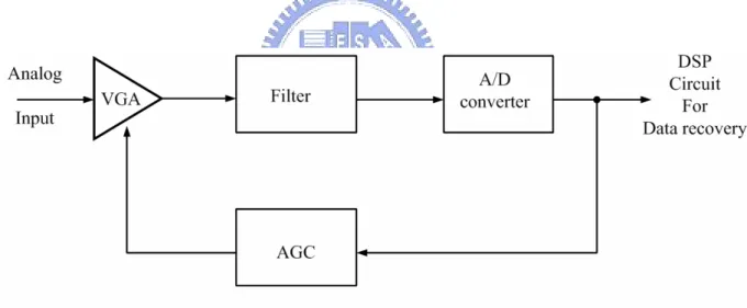
(20) 2.2. Constant Settling Time of AGC Loop. In Auto Gain Control systems as shown in Fig. 5, AGC circuits are widely applied. Usually, error free recovery of data from the input signal cannot occur until the AGC circuit has adjusted the amplitude of the incoming signal. Such amplitude acquisition usually occurs during a preamble where known data are transmitted. The preamble duration must exceed the acquisition or settling time of the AGC loop, but its duration should be minimized for efficient use of the channel bandwidth. If the AGC circuit is designed such that the acquisition time is a function of the input amplitude, then the preamble is forced to be longer in duration than the slowest possible AGC circuit acquisition time. Consequently, to optimize system performance, the AGC loop settling time should be well defined and signal independent.. Figure 5. Block diagram of a front end circuit.. The AGC loop depicted in Fig. 6 consists of a variable gain amplifier (VGA), a peak detector, and a loop filter. The AGC loop is in general a nonlinear system having a gain acquisition settling time that is input signal level dependent. With the addition of the 8.
(21) Figure 6. Block diagram of an AGC circuit.. logarithmic function shown in dotted lines and appropriate design of the loop components, the AGC system can operate linearly in decibels. This simply means that if the amplitude of the input and output signals of the AGC are expressed in decibels (dB), then the system response can be made linear with respect to these quantities. The derivations that follow will make these issues clear. By the Fig. 6,the gain of the VGA, F(Vc) is controlled with the voltage signal Vc The peak detector and loop filter form a feedback circuit that monitors the peak amplitude, Aout, of the output signal Vout and adjusts the VGA gain until the measured peak amplitude ,Vp, is made equal to the DC reference voltage ,VREF. The output of the AGC circuit is simply the gain times the input signal: Vout(t) = F(Vc)Vin(t). Since the feedback loop only responds to the peak amplitude, the amplitude of Vout is. Aout = F (Vc ) Ain. (2-3). Where Ain is the peak amplitude of Vin. The equivalent representation model of an AGC circuit, shown in Fig. 7, is derived as follows. First, the feedback loop of an AGC circuit only operates on signal amplitudes; hence the AGC input and output signals are represented only in terms of their amplitudes Ain(t) and Aout(t) respectively. Second, since the VGA multiplies the input amplitude, Ain, by F(Vc) as shown 9.
(22) Figure 7. Model of generalized AGC circuit.. in (2-3), an equivalent representation is. ⎡ Ain ⎤ Aout = Pv1 exp ⎢ln[ F (Vc )] + ln( )⎥ P v 1 ⎣ ⎦. (2-4). Pv1 is a constant with the same units as Ain and Aout (e.g., volts). The AGC model in Fig. 7 uses (2-4), but duplicates the Pv1 exp() function inside and outside the outlined block so x(t) that y(t) and represent the input and output amplitudes of the AGC, expressed in decibels within a constant of proportionality. Similarly, the z input shown is the value of VREF expressed in dB within a constant. The peak detector in Fig. 6 will be assumed to extract the peak amplitude of Vout(t) linearly and much faster than the basic operation of the loop so that Vp=Aout. Hence, the peak detector is not explicitly shown in Fig. 7. Finally, the loop filter in Fig. 6 is shown as an integrator in Fig. 7, with H(s) = GM2/sC. The model in Fig. 7 helps to simplify the mathematical derivations in this section and aids intuition. Constant settling time operation of the AGC circuit simply requires that the 10.
(23) system enclosed in dotted lines with x(t) input and output y(t) be linear. Since x(t) is the input amplitude, Ain(t) in decibels and y(t) is the output amplitude Aout(t) in dB, then a linear response from x(t) to y(t) means the AGC circuit’s amplitude response from input to output will be linear in dB. The classical result for constant settling time of the AGC loop will be derived next and will include the logarithmic amplifier shown with dotted lines in Fig. 6. Results of these derivations will be used in the next section where generalized constraints for constant settling time are developed. The output y(t) in Fig. 7 is. y (t ) = x (t ) + ln F (Vc ). (2-5). The control voltage Vc is derived as t. {. }. GM 2 Pv1e z − Pv 2 ln[ e y (τ ) ] dτ C 0. Vc (t ) = ∫. (2-6). Taking the derivative of (2-5) and substituting in the derivative of (2-6), the following expression is obtained:. dy dx 1 dF G M 2 = + [ Pv1e z − Pv 2 ln e y ( t ) ] dt dt F (Vc ) dVc C dx 1 dF G M 2 = + [VREF − Pv 2 y (t )] dt F (Vc ) dVc C. (2-7). Equation (2-7) describes a nonlinear system response of y(t) to an input x(t) unless constraints are placed on the functions. Many constraints exist, but here those with practical circuit implementations are analyzed. The first step toward obtaining a linear relationship between x(t) and y(t) is to force the coefficient in the second term of (2-7) to equal a constant, Px,. 1 dF G M 2 = px F (Vc ) dVc C 11. (2-8).
(24) And equation (2-7) can be rewritten as. dy dx + Px Pv 2 y (t ) = + PxV REF dt dt. (2-9). Equation (2-9) describes a first-order linear system having a high pass response from the input x(t) to y(t) the output The time constant,τ, of the system is given by. ⎡ 1 ⎤ 1 dF G M 2 =⎢ τ = Pv 2 ⎥ Px Pv 2 ⎣ F (Vc ) dVc C ⎦. −1. (2-10). The classical criterion for constant settling time of the AGC loop assumes that GM2 and C are constants in (2-8) and (2-10), forcing the gain control function of the VGA to satisfy the following constraint:. 1 dF = PG1 F (Vc ) dVc. (2-11). Where PG1 is constant:. 1 dF = PG1 F (Vc ) dVc dF = PG1 dVc F (Vc ) dF ∫ F (Vc ) = ∫ PG1dVc ln[F (Vc )] = PG1Vc + C. (2-12). F (Vc ) = e PG 1Vc +C = e C e PG 1Vc = PG 2 e PG 1Vc Where PG2=eC is a constant of integration. One can easily determine that the gain in decibels (dB) should vary linearly with the control signal, Vc. Using (2-12) for an exponential VGA gain characteristic and (2-10), the time constant of the AGC loop with a logarithmic amplifier included, is show as equation (2-13).. 12.
(25) τ exp −log =. C G M PG1 PG 2. (2-13). With the constraints provided, the AGC loop will operate as a linear system in decibels for any change in input amplitude. By taking inverse of equation (2-13) and multiplying 2π, we can get the. f T = PG1 PG 2. GM 2πC. (2-14). It is the locked bandwidth of AGC loop.. z Without Logarithmic Amplifier In many AGC systems, the logarithmic amplifier shown with dotted lines in Fig. 6 is omitted. The objective of constant settling time can still be met under certain small-signal approximations. The key assumption in the following derivation will be that the output amplitude of the AGC loop is operating near its fully converged state (ie. Aout ~ VREF) . Equation (2-7) can be rewritten as:. dy dx = + Px [V REF − PV 1e y ( t ) ] dt dt. (2-15). The system response is nonlinear even with a constant Px due to ey(t). If the changes in the input and output amplitude levels are small, then the exponential ey(t) in (2-25) can be expanded in a Taylor series. Assume that the AGC loop is initially converged, such that the output amplitude, equals VREF Referring to Fig. 7, this implies that y(t)=z and the Taylor series expansion is. e y ( t ) ≈ e z [1 + y (t ) − z + L]. (2-16). And equation (2-16) can be represented as. V dy dx dx + PxVVREF y (t ) = + PxV REF z = + PxV REF ln( REF ) dt dt dt Pv1 13. (2-17).
(26) That will be the same as equation (2-9), the first-order linear system is a high pass response with a time constant of. ⎡ 1 ⎤ 1 dF G M 2 =⎢ τ = V REF ⎥ PxVVREF ⎣ F (Vc ) dVc C ⎦. −1. (2-18). GM2 and C are linear and time invariant, then the constraint on constant settling time for the AGC loop is that the VGA has an exponential gain control characteristic as in (2-12). Under these conditions, the AGC loop without a logarithmic amplifier has a time constant given by. τ exp =. C G M PG1V REF. (2-19). From the above explanation, we can see that an exponential gain characteristic VGA is necessary for a constant settling time AGC loop [3].. 2.3. Pseudo Exponential Technique. The exponential gain to linear control voltage characteristic is necessary for auto gain control loop to minimize variations in the output voltage and had be discussed in section 2.2. In, CMOS devices, there is no logarithmic device characteristic which like bipolar device. In bipolar or BiCMOS technology, the exponential function is readily available with the base-emitter voltage to collector current characteristic. Here we present a methodology for generating the desired exponential transfer characteristics intrinsically using only MOS devices within the variable gain amplifier [9]. If the gain function is of the form ew, the exponential function can be approximated as equation (2-20).. 14.
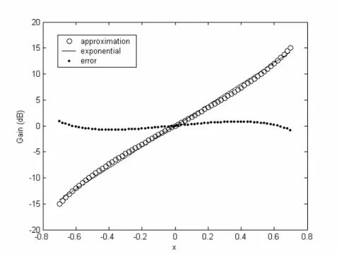
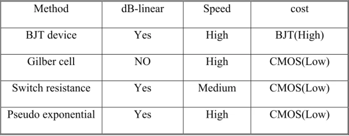
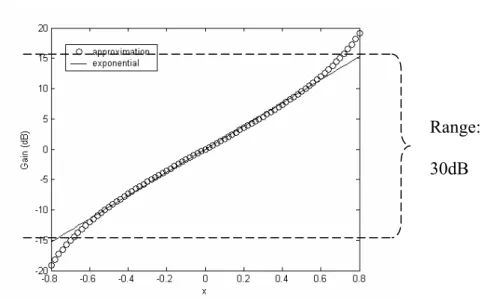
(27) Figure 8. Pseudo exponential gain versus control parameter.. ⎛1+ w / 2 ⎞ ⎛1+ x ⎞ ew ≈ ⎜ ⎟=⎜ ⎟ = Gain ⎝1− w / 2 ⎠ ⎝1− x ⎠ 2 ( 1 + x) Gain range = (1 − x )2. (2-20). (2-21). The expression is plotted in Fig. 8, where the y scale is in dB’s. It is possible that the gain expression in equation (2-20) provides the necessary exponential transfer characteristics and shows good match for -0.7 < x < 0.7. Further, it can be shown that the maximum gain range is given by equation (2-21). Therefore, for a gain range of 30dB the value of x needs to be varied from -0.7 to +0.7. As just mentioned, the exponential characteristic matches fairly well within this range. Outside this region (-0.7 < x < 0.7) the rate of change in gain will be even more rapid. Table1 lists the comparison between several methods. From the comparison result, we can see that the Pseudo exponential method is best choice for high speed linear in-dB variable gain amplifier. 15.
(28) Method. dB-linear. Speed. cost. BJT device. Yes. High. BJT(High). Gilber cell. NO. High. CMOS(Low). Switch resistance. Yes. Medium. CMOS(Low). Pseudo exponential. Yes. High. CMOS(Low). Table 1.. Comparison between several VGA method. 16.
(29) Chapter 3 Novel High Dynamic Range Technique This chapter presents a novel variable gain amplifier (VGA) circuit for high dynamic range applications. Section 3.1 addresses one example of pseudo-exponential topologies to approximate its gain polynomial to exponential. The proposed VGA will employ the concept of the referenced circuit as shown in section 3.1. The proposed pseudo-exponential gain control technique is presented to enhance the gain range and is described in section 3.2. The comparison between conventional methodology and proposed methodology will be shown in section 3.3.. 3.1. Conventional Approach. A conventional topology for pseudo-exponential gain control using MOS transistors had been developed as shown in Fig. 9 [5]. The amplifier can be treated as a source-couple pair with diode connected load. The output impedance is determined by the diode connected load (1/gm) since the gain will be equivalent to input and load transconductance ratio. The conventional circuit consists of three parts, namely, gain cell (M1-M8), gain control clock (M11-M14) and common mode feedback. The gain cell possesses the pseudo exponential gain transfer curve with respect to the linear gain control signal that is generated from the gain control cell. Common mode feedback circuit is used to stabilize the output. 17.
(30) Figure 9. Schematic of the conventional variable gain amplifier.[5]. common mode level because all circuits are fully differential structure. To control amplifier gain, the transconductance of MOS input and load transistor is varied with the change of control current. The currents through input pair and load are constant and equal to the current of upper PMOS (M7 and M8). The gain control block is formed by another PMOS source couple pair (M11 and M12). The gain control mechanism can be achieved by mirroring the gain control block differential output currents to the tail current source (M5 and M6) of input source coupled pair and load respectively. Current mirrors (M5, M6, M13, and M14) are long channel devices for good precision. The gain is hence proportional to the square root of the approximated polynomial as shown in equation (3-1).. Gain = = =. gm in gm load. µC ox (W / L ) in ⋅ I in µC ox (W / L ) load ⋅ I load I + Ic µC ox (W / L ) in ⋅ b Ib − Ic µC ox (W / L ) load. =K⋅. 1+ x 1− x 18. (3-1).
(31) Range: 15dB. Figure 10 Conventional circuit approximation on a decibel scale. In equation (3-1), the transconductance of MOS input and load transistor varies with the change of current. The gain is hence limited by the square-root nature of the device. The maximum gain range is shown in Fig. 10 which is half of the ideal approximation equation since the gain is proportional to the square root of the approximated polynomial. From Fig. 10, where variable x is the ratio of the additional current Ic to DC bias current Ib when control signal is applied. Equation (3-1) has the form like Equation (2-20) with power is 1/2. The polynomial matches a logarithmic function reasonably for parameter x up to ±0.7, however, with the power of 1/2 result in the maximum gain range is limited to about 15 dB per stage.. 3.2. Proposed Approach. The proposed approach aims to improve the gain range by canceling the square-root of equation (3-1). In the conventional approach, the transconductance is varied with the change of control current, resulting in square-root relation. In the proposed method, we replace the controlled current with the varied voltage. The concept can be expressed as following: 19.
(32) Figure 11 The concept of the proposed methodology The pseudo exponential technique is based on equation (1+x) / (1-x). If we control the gate voltage of NMOS and PMOS current source at the same time, we will increase (decrease) NMOS over driver voltage and decrease (increase) PMOS over driver voltage at the same time. For example is shown in Fig. 11, when ∆X is increased, Vgsn and Vsgp will be increased and decreased at the same time. Now we will apply this method to realize the pseudo exponential variable gain amplifier. Assume square law relation of drain current and gate-over drive voltage is applied, the transconductance isproportion to the over voltage of current source. gain =. gm in = gm load. (W / L )i (W / L )l. ⎛W ⎞ 2 I M = µC ox ⎜ ⎟(Vctrl − Vt ) L ⎝ ⎠. ⎛1+ x ⎞ gain = k × ⎜ ⎟ ⎝1− x ⎠ ⎛1+ x ⎞ gain range = ⎜ ⎟ ⎝1− x ⎠. 2. I Msn I Msp. (3-2). (3-3). (3-4). From equation (3-4), if we replace the control parameter with over voltage then the gain 20.
(33) Figure 12 Proposed technique. will never limit by the square root again. The proposed amplifier for enhancing maximum gain range of one stage is shown in Fig. 12. The gain circuit in the proposed topology is like the referenced VGA circuit, which a source-coupled pair serves as input transconductance stage, and diode-connected transistors are used for the loads. A DC-level shift block is applied for the suitable bias condition of NMOS and PMOS current sources.. The ratio of input to load transconductances can be. expressed as following: gain = =. gminput gmload. =. I µCox (W / L)i × Msn I Msp µCox (W / L) l. µCox (W / L)i µCox (W / L) Msn ⎛⎜ Vctrl − Vshf − Vtn + ∆V ⎞⎟ ⋅ × µCox (W / L) l µCox (W / L) Msp ⎜⎝ VDD − Vctrl − Vtp − ∆V ⎟⎠. (3-5). From equation (3-5), the transconductances of input and load transistors are designed to vary in proportional to the change of the control voltage. By satisfying the condition as,. Vctrl − Vshf − Vtn = VDD − Vctrl − Vtp 21. (3-6).
(34) Range: Range: 30dB 30dB. Figure 13 Proposed simulation on a decibel scale. equation (3-5) can be further simplified.. 1+ x ) 1− x ∆V ∆V = where x = Vctrl − Vshf − Vtn VDD − Vctrl − Vtp gain = K × (. K=. (3-7). µC ox (W / L) i µC ox (W / L) Msn ⋅ µC ox (W / L) l µC ox (W / L) Msp. From the above description, the pseudo exponential equation (1+x) / (1-x) is satisfied under the proposed method. The ideal simulation result is shown as Fig. 13 and the gain will be 30 dB dynamic ranges. We will make a comparison in next section and explain the benefit of the wide dynamic gain range.. 3.3. Comparison. A. Gain Range Figure 14 shows the comparison between the conventional pseudo-exponential polynomial, ideal logarithmic curve, and the polynomial of proposed approximation. This work fits the ideal exponential curve in the range of parameter x value between 0.7 and -0.7. 22.
(35) Figure 14 Real term generated by inductively source degeneration. Since the gain of proposed topology is in proportional to (1 + x) / (1 - x) rather than its square root, the maximum gain range achieved is then doubled to about 30 dB. To get the same gain control range, only half the numbers of amplifier stages are required by using the proposed topology. The reduction of cascaded stages not only reduces the power consumption but also increases the 3-dB bandwidth.. B. Bandwidth Fig. 9 and Fig. 12 show the conventional and proposed VGA circuit. There are no high impedance nodes in the signal path. The only pole that limits the bandwidth of the VGA is at the output node. The bandwidth of this amplifier is determined by load transconductance and output node parasitic capacitance, as f BW =. g 1 = mload 2πRC 2πC out. (3-8). Both conventional and proposed circuits apply the diode connected load. The bandwidth of circuits will be limited to the same condition as shown in equation (3-8). In the proposed circuit, the dynamic gain range is increased without decreasing the bandwidth for one stage. 23.
(36) We can extend the bandwidth by increased the gmload, but the gain decreases at the same time.. C. Output Swing In the conventional amplifier, there are three cascode devices which are composed of a NMOS tail current source, a PMOS tail current source and differential pair input stage with transconductance loads. The following equation proves the maximum output voltage swing constraint. V swing = V DD − Vt − 3∆V. (3-9). Where ∆V is the overdrive voltage for a device operated in saturation region. Assume Vt~0.5V, ∆V~0.3V and VDD=1.8. The Vswing will be 0.4 Vpp. In the proposed amplifier, there are four cascade devices composed of a NMOS tail current source, a PMOS tail current source, input NMOS differential pair and PMOS transconductance loads. The four cascode devices will reduce the output swing. The output swing voltage will be shown as following equation. V swing = V DD − Vt − 4∆V. (3-10). Compared with the conventional circuit, the output swing a ∆V less. The Vswing will be 0.1 Vpp which is a very small voltage. The small output swing is a serious problem for system. In order to overcome this drawback, a post amplifier can be added after the VGA circuit. The overall architecture of VGA system will be discussed in chapter 4.. D. Gain Error The gain error is related with the gain equation. The gain error of the equation (1 + x) / (1 - x) is double of the equation [(1 + x) / (1 - x)] 0.5 and the latter one has gain error about 0.5dB in appropriate design. Hence the novel pseudo exponential will get more gain error. But in a wide gain range system, the dynamic gain range must more than 50dB. Total gain equation is [(1 + x) / (1 - x)] 2. Under the same gain equation, two circuits have the same gain. 24.
(37) error.. 3.4. Deep Submicron Effect In 0.18µm CMOS process, since scaling has substantially deviated from the. constant-field scenario, small-geometry devices experience significant mobility degradation. An empirical equation modeling this effect is:. µ eff =. µ0. 1 + θ (VGS − VTH ). (3-11). And the square-law current equation must be rewrite as:. ID =. µ 0Cox 1 W (VGS − VTH ) 2 2 1 + θ (VGS − VTH ) L. (3-12). We can drive the θ from the BSIM3V3 model Æ .Mobmod=2. µ eff =. µ0. V − VTH V − VTH 2 1 + (U a + U cVbseff )( GS ) + U b ( GS ) TOX TOX. (3-13). From UMC .18 model, we can find following parameter: Ua、Ub、Uc and TOX. For Vbs=0, the θ can be derived about 0.22 ~ 0.24. Assuming θ(VGS-VTH)<<1, we obtain:. W 1 µ 0 C ox [1 − θ (VGS − VTH )](VGS − VTH ) 2 L 2 1 W ≈ µ 0 Cox [(VGS − VTH ) 2 − θ (VGS − VTH ) 3 ] 2 L. ID ≈. The pseudo exponential gain function is rewired as following:. 25. (3-14).
(38) gain =. gminput gmload. =. I µC ox (W / L) i × Msn I Msp µC ox (W / L) l. =. µC ox (W / L) i µC ox (W / L) Msn ⎛⎜ Vctrl − Vshf − Vtn + ∆V ⋅ × µC ox (W / L) l µC ox (W / L) Msp ⎜⎝ VDD − Vctrl − Vtp − ∆V. ⎞ 1 − θ n (VGSn − VTHn ) ⎟× ⎟ 1 − θ (V − V ) p SGp THp ⎠. =. µC ox (W / L) i µC ox (W / L) Msn ⎛⎜ Vctrl − Vshf − Vtn + ∆V ⋅ × µC ox (W / L) l µC ox (W / L) Msp ⎜⎝ VDD − Vctrl − Vtp − ∆V. ⎞ 1 − θ n (Vctrl − Vshf − Vtn + ∆V ) ⎟× ⎟ 1 − θ (VDD − Vctrl − Vtp − ∆V ) p ⎠. θn is about 0.22 ~ 0.24 and θp is about 0.35 ~ 0.36. In 0.18µm CMOS process, we can derive the error term. 1 − θ n (Vctrl − Vshf − Vtn + ∆V ) 1 − θ p (VDD − Vctrl − Vtp − ∆V ). which influence the pseudo exponential equation. The gain range may be decreased about 6%. The gain range decreases due to deep submicron effect is about 0.6dB for one stage.. 26.
(39) Chapter 4 Variable Gain Amplifier Design Since the proposed high dynamic VGA performs well in the exponential approximation, the VGA circuit is employed in the UWB system for verification and will be discussed in this chapter. Section 4.1 introduces in brief the MutiBand OFDM proposal and focuses on gain range related information. Section 4.2 discusses the variable gain amplifier architecture for UWB system. Section 4.3 discusses the variable gain amplifier circuit design. Section 4.4 analyses the post amplifier circuit. Section 4.5 discusses the offset cancellation technique. The simulation results for VGA application in the UWB system is shown in section 4.6.. 4.1. MB-OFDM Proposal Brief. In the MB-OFDM proposal [11], the FCC approved spectrum, 3.1-10.6 GHz, is divided into 14 bands where each band has bandwidth of 528 MHz. As shown in Figure 1, the 14 bands are categorized into 5 band groups where a time-frequency code (TFC) is utilized to interleave coded data over up to three frequency bands. Each band uses a total of 122 modulated and pilot subcarriers out of a total of 128 subcarriers whose bandwidth is 4.125 MHz each. The OFDM subcarriers are modulated using QPSK. To avoid difficulties in DAC and ADC offsets and carrier feed-through in the RF system, the subcarrier falling at DC (0th subcarrier) is not used. The support of transmitting and receiving at data rates of 53.3, 110, 27.
(40) Figure 15 Transmitter power spectral density mask in MB OFDM proposal.. Table 2.. Data Rate (Mb/s). Minimum Sensitivity for Mode 1 (dBm). 53.3. -83.6. 80. -81.6. 110. -80.5. 160. -78.6. 200. -77.2. 320. -75.5. 400. -74.2. 480. -72.6. Receiver performance requirement in MB OFDM proposal.. and 200 Mb/s is mandatory, while the maximum capability can achieve 480 Mb/s. Devices operating in band group #1 are denoted Mode 1 devices, and it shall be mandatory for all devices to support Mode 1 operation, with support for the other band groups being optional and added in the future. The transmitted spectrum shall have a 0 dBr (dB relative to the maximum spectral density of the signal) bandwidth not exceeding 260 MHz, –12 dBr at 285 MHz frequency offset, and –20 dBr at 330 MHz frequency offset and above. The transmitted spectral density of the transmitted signal mask shall fall within the spectral, as shown in Fig.15. For a packet error rate (PER) of less than 8% with a PSDU of 1024 bytes, the minimum receiver sensitivity numbers for the various rates and modes are listed in Table 2. In the MB-OFDM proposal, the output power of transmitter is defined as -10dBm. Assume 28.
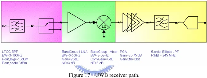
(41) Figure 16 System architecture of UWB transceiver.. Figure 17 UWB receiver path. the channel loss is about 30dB, then the maximum power will be revived by receiver is -40dBm. From Table.1, the minimum sensitive is -83.6dBm. Hence the input range is -40dBm ~ -83.6dBm for a UWB receiver. Direct-conversion is adopted in the system architecture as shown in Figure 16. The bulky image rejection filters are not necessary any more and system-on-chip (SOC) integration is more accessible with this more compact architecture. Besides, it is more important that power consumption can be much reduced. Figure 17 shows the reciver building blocks and module specifications. We plan a receiver path from LNA to A/D converter as shown in Fig. 17. The VGA block will provide a wide dynamic range from 25 to 75 dB. In following section, we will introduce the VGA block.. 29.
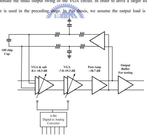
(42) 4.2. Variable Gain Amplifier Architecture. Fig. 4 shows the block diagram of the VGA design. The VGA consists of two cascaded pseudo-exponential gain cells with a offset subtractor. The input referred offset voltage is derived from output common mode voltage by a 2nd order low-pass filter, and fed back to the offset substrator at the input port. The input referred offset voltage is reduced by the feedback amount with offset compensation loop. The dominant pole of the loop filter is introduced by an external capacitor with on chip resistor to save chip area [12]. In order to improve the linearity of over all VGA architecture, a post amplifier is connected after the variable gain amplifier. A post amplifier will provide a gain about 38.7dB and will compensate the small output swing of the VGA circuit. In order to drive a larger load, a buffer is used in the preceding stage. In this thesis, we assume the output load is 10p.. Figure 18 Variable gain amplifier architecture.. 30.
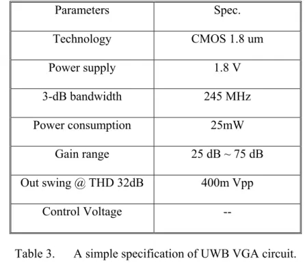
(43) Parameters. Spec.. Technology. CMOS 1.8 um. Power supply. 1.8 V. 3-dB bandwidth. 245 MHz. Power consumption. 25mW. Gain range. 25 dB ~ 75 dB. Out swing @ THD 32dB. 400m Vpp. Control Voltage. --. Table 3. Process Node 90 nm 130 nm. A simple specification of UWB VGA circuit. Rate (Mb/s) 110 200 480 110 200 480. Table 4.. Transmit 93 mW 93 mW 145 mW 117 mW 117 mW 180 mW. Receive 155 mW 169 mW 236 mW 205 mW 227 mW 323 mW. Power consumption for Mode1 DEV(3-Band).. A simple specification for an UWB VGA circuit is shown as Table.2, the minimum bandwidth is required 245MHz. Because the resolution of A/D converter is 5bits, hence the total harmonic destruction (THD) is required just more than 32dB. There is no specification about the power consumption, but Table 3 shows power consumption for Mode1 DEV(3-Band). As a consequence, a low power VGA of ultra-wide band cover all the frequency of interest, and according system budget the total power consumption of VGA should be limited in 20mW.. A lot of power will be consumed in output buffer, and the. distribution of power consumption will be discussed in section 4.4.. 31.
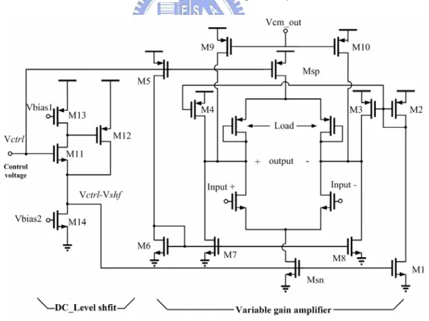
(44) 4.3. Variable Gain Amplifier Circuit. Fig. 19 shows the complete schematic of proposed VGA with a DC-level shift. In order to get better settling time performance and current balance, transistors M1 - M4 are the current mirror for transistor Msn and transistors M5 - M8 are the current mirror for transistor Msp, respectively. The M9 and M10 are adjusted by the common-mode feedback (CMFB) unit. Transistors M11 - M14 are used to perform voltage buffer and provide voltage level shift [13]. Transistors Msn and Msp are used to control input and load transconductance together with the control voltage as mentioned earlier. Compare with Fig. 12, eight transistors M1 - M8 are added in Fig. 19 to balance the current when gain is varied. Because the gain is proportion to the ratio of transconductance, we need to control the drain current of Msn and Msp to vary the transconductance of input. Figure 19 Schematic of the variable gain amplifier.. 32.
(45) Figure 20 Common mode feedback amplifier. and load transistor. Now let us discuss about the circuit without transistors M1- M8. In high gain mode, Vctrl is increased and the over driver voltage of Msn is increased and Mps is decreased. Under this condition, the tail current source Msn will be driven to linear range and the pseudo exponential will never existence. There is another important parameter we must pay attention, in equation (3-7). The gain range of pseudo exponential equation will be -15dB ~ 15dB, if the parameter k equate one in equation (3-7). In our UWB system requirement, VGA’s gain range must be 25dB ~ 75dB. Hence we must shift the gain range of pseudo exponential equation. In this thesis the parameter k will be designed about 2.4 and the gain range of signal stage VGA circuit will be -7.8dB ~ 19.3dB. By this mean, there is about 27dB dynamic gain range for one stage VGA and only two VGA stages are required to satisfy the UWB system specification. If we chose the conventional VGA circuit we need four stages to satisfy the UWB system which more than 45dB dynamic gain range is required. A common mode feedback circuit is used to stabilize the output common mode level, since all the circuits are fully differential. Output DC level variation is important in 33.
(46) Figure 21 Signal stage VGA simulation. DC-coupled multi-stage VGA design. If the VGA cannot provide a stable and accurate output DC level, the following stages will be biased at wrong operation point under different gain settings. The output of the common mode feedback circuit is used to adjust the bias current through the transistors M9 and M10. The diagram of the common mode feedback unit is shown in Fig. 20. The compensative resistance is implemented by a transistor Mr operating in triode region [14]. This common mode amplifier has one benefit which can provide infinite impedance for the output node of the VGA circuit, since the gain variation is related with the output impedance in the VGA circuit. Hence the output connected to the gate of the transistor will not affect the gain of the VGA circuit. Fig. 21 shows the simulation curve of one stage VGA circuit. The dynamic gain is -7.8dB ~ 19.3dB. The combination of the VGA and CMFB circuits is a negative feedback structure. Hence the stability problem must be discussed in this feedback circuit. Fig. 22 is a circuit diagram for stability simulation; we interrupt the feedback path and put the gate capacitance of transistors M9 and M10 as an output load for CMFB. Fig. 23 & 24 are the phase margin simulation result for high gain and low gain mode, larger phase margin is necessary to avoid oscillate issue. From the Fig. 23 & 24 phase margins are 103deg and 117deg and we can make sure that this feedback structure is a stable structure.. 34.
(47) Figure 22 Stability simulation setup.. Figure 23 Phase margin simulation (high gain).. Figure 24 Phase margin simulation (low gain). 35.
(48) Figure 25 Schematic of the post amplifier.. 4.4. Post Amplifier & Buffer. The small output swing is a serious problem for UWB systems. In order to conquer this drawback, a post amplifier will be added after the VGA circuit. The post amplifier provides a 38.7dB gain to improve the gain range from -15.6dB ~ 37.6dB to 23dB ~ 76.3dB. A voltage gain of 38.7dB over a large bandwidth of 250MHz requires the use of wide-band design technique. Fig. 25 shows the post amplifier circuit, our design uses a two stage shunt feedback cell. The shunt feedback resistor RG lowers the resistance at the drains of both M3 and M7, and thus pushes the pole frequencies at the critical nodes and extends the bandwidth; it also sets the amplifier voltage gain. A cascode connection is used in the first stage to suppress the Miller multiplied Cgd of M1 from producing an undesirable capacitive loading at 36.
(49) the input node, which only worsens the noise. To further enhance signal bandwidth, inductive loads at second stage are utilized to partially trim out parasitic capacitance at the drain of M7 and M8. In this design, active inductors are employed instead of passive spiral inductors for the latter are in general bulky and contributes significant parasitic capacitance. The active inductor is made up of an NMOS and a resistor, connected as M9 + M10 and M11 + M12. The NMOS is operated in saturation and the resistor is implemented using a PMOS operating in triode region. In addition, the current injection device Mb1 and Mb2 are incorporated to mitigate DC drop caused by active inductors. This technique increases voltage headroom. The equivalent inductance of the proposed active inductors can be approximated by: L≈. where. z1 =. 1. (4-1). z z1 gm(1 − 1 ) p1. 1 R (C gs + C µ ). p1 =. gm C gs + C L + gmRC µ. Gm, Cgs, Cμ and CL are the transconductance, parasitic capacitance and source loading capacitance of M9 and M11. Fig. 26 shows the simulated gain is 38.7dB and bandwidth is 657MHz. The stability simulation is shown in Fig. 27. Where phase margin is about 50deg.. Figure 26 Frequency response of the post amplifier. 37.
(50) Figure 27 Phase margin of the post amplifier.. Figure 28 (a) Conventional source follower, (b) Super source follower circuit. A source follower circuit is used as an output buffer as shown in Fig. 28(a). Because MOS transistors usually have much lower transconductance than the bipolar counterparts, this output resistance maybe too high for some applications, especially when a resistive load must be driven. One way to reduce the output resistance is to increase the transconductance by increasing the W/L ratio of the source follower and its dc bias current.. 38.
(51) Figure 29 Small signal mode of the super source follower. However, this approach requires a proportionate increase in the area and power dissipation to reduce output impedance. To minimize the area and power dissipation required to reach a given output resistance, super source follower configuration is employed as shown in Fig. 28 (b). This circuit uses negative feedback through M2 to reduce the output resistance. Small signal mode of the super source follower circuit is shown in Fig. 29. From KCL at drain of M1, we can derive the following equation: V gs 3 = − gm1V gs1 ro 2. (4-2). From KCL at output node: Vout = ( gm1V gs1 − gm3V gs 3 ) ro 4 = gm1V gs1 (1 + gm3V gs 3 ) ro 4. (4-3). = gm1 (1 + gm3 ro 2 )ro 4 (Vin − Vout ). From equation (4-3) the Vout / Vin ratio can be shown as following gm1 (1 + gm3 ro 2 )ro 4 Vout = Vin 1 + gm1 (1 + gm3 ro 2 )ro 4 =. (4-4). ro 4 ro 4 +. 1 gm eff. and the equivalent transconductance gmeff is : gmeff = gm1 (1 + gm3 ro 2 ). 39. (4-5).
(52) Figure 30 Simulation result of the output buffer with 10pF load. Comparing a simple source follower and super source follower shows that the deviation of this gain from unity is greater than that of a simple source follower, if gm3ro2 >> 1. The buffer is simulated with an off-chip capacitive load as large as 10pF. The simulation result is shown in Fig. 30, the loss of the output buffer is about 1.38dB and bandwidth is 750MHz with 10pF load. The power consumption is about 10mW. We use the super source follower technique to provide very small output impedance; hence the output buffer can drive a large capacitive load.. 4.5. Offset Cancellation. As shown in Fig. 18, the input referred offset voltage is derived from post amplifier output common mode voltages by a 2nd order low pass filter and feedback to the offset substractor at the input port. By this means, VGA’s input referred offset voltage is reduced by 1/β after offset compensation, where β is the DC gain of the feedback network. The dominant pole of the loop filter is introduced by an external capacitor with an on-chip resistor to save chip area and extend fL-3dB. The gain cell in the feedback path isolates capacitive loading introduced by the feedback filter from the output port. From another. 40.
(53) Figure 31 The gain cell in the feedback path. prospective, it also enhances offset suppression and input sensitivity of VGA by β, which is shown in Fig. 31. In order to reduce the output capacitive load of the post amplifier, the cascode structure is used in this gain cell design. The transistors M7 and M8 are operated in triode region, and then can be seen as active resistance. The transistors M5 – M8 establish a resistive CMFB load, hence this circuit doesn’t need another CMFB amplifier to stablize the output DC-level. The input stage of VGA is shown in Fig. 32, which plays an important role in isolating loading effects introduced by the loop filter. The source coupled pair in the input stage is decomposed into 4 transistors so as to function as an input buffer and an offset substractor simultaneously. The offset voltage derived from the low pass loop filter is converted to a compensating current and subtracted from input signal at the input node of a regular cascode gain stage. Because of adding the transistors M21 and M22, the gain range of the first stage will be effected and never be same as the second VGA stage introduced in section 4.2. The gain range of input stage is shifted -8.1dB ~ 18.3dB and simulation result is shown in Fig.33.. 41.
(54) Figure 32 VGA input stage and offset substractor.. Figure 33 Simulation result of the input stage and offset substractor.. 4.6. Digital control circuit. Two kinds of VGAs are discussed in this thesis. The first kind VGA is voltage control type which has be introduced in above. The control signal of the voltage control VGA is directed. 42.
(55) Figure 34 Linear load which is a back-to-back connect of current mirrors. controlled by voltage. In this session, we will introduce the Programmable Gain Amplifier (PGA is a digital control VGA) circuit for some application. The digital control circuit includes the linear load and digital to analog converter. The digital to analog converter will provide current which across the linear load and will be converted to voltage signal. Now, we will present the linear load used to convert current to voltage. The linear load used to generate the control voltage is a back-to-back connection of current mirror [15]. The circuit diagram is shown in Fig.34. The input impedance will be proved as following: The drain current of the NMOS is the sum of the PMOS and DAC output current: In = I p + Ic k k (Vout − Vtn) 2 = (V DD − Vout − Vtp ) 2 + I c 2 2. (4-6). from equation (4-6), we can further express as following: (Vout − Vtn) 2 − (V DD − Vout − Vtp ) 2 = 2Vout − (V DD + Vtn − Vtp ) =. 43. k (V DD. 2I c k. 2I c − Vtp − Vtn). (4-7).
(56) Figure 35 A 6-bit current steering DAC.. and the output voltage Vout can be expressed as following: Vout =. k (V DD. (V DD + Vtn − Vtp ) Ic + 2 − Vtp − Vtn). (4-8). Input impedance is proved to be a constant: Rin =. 1 ∂Vout = ∂I c k (V DD − Vtp − Vtn). (4-9). The constant impedance can convert the current signal to voltage signal linearly. The control signal IC is a bi-directional current. To support the digital control, a digital-to-analog converter (DAC) can be used and is shown as in Fig.35. A simple binary-weighted current source type bipolar DAC has been chosen for that proposes. The DAC supports a linear current IC which is proportional to the numerical value represented by the digital control bits. IC is then converted by the linear load to a control voltage Vctrl.. 44.
(57) Chapter 5 Implementation and Experimental Results While device scaling has enhanced the speed of transistors, unwanted interaction between different sections of integrated circuits as well as non-idealities in the layout and packaging increasingly limit both the speed and the precision of such systems. Today’s analog circuit design is very heavily influenced by layout and packaging. The proposed wide-dynamic variable gain amplifier design is to be implemented in CMOS and packaged in QFN. This chapter presents the implementation results of the VGA. Section 5.1 shows the over all VGA circuit simulation. Section 5.2 presents the chip layout of the proposed VGA and the post-layout simulation results. Section 5.3 analyzes ESD protection architecture and describes the package model. The PCB layout is given in Section 5.4. Section 5.5 introduces the testing plan. The measurement results and analysis are shown in section 5.6. In section 5.7 we introduce the error correction method to compensate gain errors in high gain operations. Section 5.8 summarizes the proposed VGA design.. 5.1. Overall VGA Circuit Simulation. The circuit design has been described in chapter 3. Now, the overall VGA circuit simulation will be shown in this section. Fig. 36 shows the gain range simulation of the VGA architecture which includes the two stages VGA and post-amplifier. The dynamic gain 45.
(58) range is 53dB which is from 23dB ~ 76dB. Comparison with the ideal pseudo exponential. Figure 36 Dynamic gain range simulation result.. Figure 37 Frequency response simulation result. VGA which is 60 dB dynamic gain range, the proposed VGA has about 7dB dynamic gain range reduction. In high gain operations, we will present some error correction technique for compensating this mismatch in section 5.7. The frequency response shows in Fig. 37. The bandwidth varies with differential gain setting, the minimum bandwidth is under the maximum gain setting and the maximum bandwidth is under the minimum gain setting. In the worst case, the minimum bandwidth is about 275MHz which is larger than the specification 245MHz. The transient simulation is shown in Fig.38 and Fig. 39. Under the low gain condition, 46.
(59) the output swing is about 500mVpp for a single-ended output with 36dB total harmonic. Figure 38 Output swing simulation (Low gain).. Figure 39 Output swing simulation (High gain). 47.
(60) 20. 20. m7 dBm(out[::,1]). dBm(out[::,1]). 10 0 -10 -20 -30. m7. 10 0 -10 -20. -40. -30. -50. -120. -110. -100. -90. -80. -70. -60. -50. -50. -40. -30. -20. -10. 0. Power_RF. Power_RF. m7 indep(m7)=-16.000 plot_vs(dBm(out[::,1]), Power_RF)=7.848. m7 indep(m7)=-66.000 plot_vs(dBm(out[::,1]), Power_RF)=9.992. Figure 40 P1dB simulation (High gain & Low gain).. 25 20 15 23.3 10 11. 5 0. 2.3. 2 VGA. 3.3. 2.3. 2.04. sub. Post-amp βAmp. Control VGA. Buffer. Total. Figure 41 Power consumption. Parameters. Spec.. Simulation.. Technology. CMOS 0.18 um. CMOS 0.18 um. Power supply. 1.8 V. 1.8 V. 3-dB bandwidth. 245 MHz. 275 MHz. Power consumption. As small as possible. 23.3mW. Gain range. 25 dB ~ 75 dB. 23 dB ~ 76 dB. Out swing @ THD 32dB. 400m Vpp. >470m Vpp. Control Voltage. --. 0.93~1.3. Table 5.. The simulation results of UWB VGA circuit. 48.
(61) distortion (THD). Under the high gain condition, the output swing is about 470mVpp for a single-ended output with 40dB total harmonic distortion (THD). For 5-bit Analog to Digital Converter (ADC) we need more than 32dBc THD. Figure 40 is P1B simulation result. In high gain mode (~76dB), output p1dB is about 9.9 dbm. In low gain mode(~24dB), output p1dB is about 7.8 dbm. Fig.41 shows the simulation power consumption of the complete circuit. A single stage VGA dissipates 2 mW from a 1.8-V power supply and the total power consumption is 23.3 mW. In order to drive the load of testing instrument, the output buffer consumes 11mW which is the largest power dissipation of overall architecture. Table.5 shows the summary of the simulation results. The simulation results satisfy for each parameter under the comparison with the specification.. 5.2. Chip Layout and Post-Layout Simulation. The layout of an integrated circuit defines the geometries that appear on the masks used in fabrication. The geometries include n-well, gate oxide, ploysilicon, source/drain areas, nand p+ implants, interlayer contact windows, and metal layers. For the analog or RF circuit design, even with the same schematic design, different layouts will make entirely difference performance of the circuit. Therefore, the design of the layout is an important topic, especially for high frequency design. The most important things of the layout are parasitic and mismatches. For example, long metal lines will cause the parasitic capacitance and resistance thus decrease the bandwidth and gain loss of the circuit. Improper layout could result in large difference of performance between simulated and measurement result, or even result in failed circuits. The layout is following the rule that no signal returns close to its origin in order to avoid coupling back to the input. The matching. 49.
(62) and symmetry should be arranged very carefully for the differential circuit. The common-centroid layout is employed to alleviate device mismatch due to process variation. The supply power is drawn in form of power ring within the pads. The die of packaged version is to fit the standard form of the QFN-20 pin package. The pads of packaged version are ESD protected which will be introduced in the later sections. Finally, all the line widths are drawn according to following criterial, minimizing parasitic capacitance and series resistance. The DC current paths should be wide enough to prevent electro-migration. The line length of signal path should be kept as short as possible. The VGA circuit layout is shown in Fig. 42, where variable gain-amplifier, DC-offset. Figure 42 Circuit layout of the voltage control VGA.. Figure 43 Circuit layout of the Digital control VGA (packaged version). 50.
(63) cancellation, β-amplifier, post amplifier, DC-level shifter and output buffer circuit can be found. The total area is 0.5 × 0.45 mm2. Fig. 43 shows the packaged version with the DAC circuit which die area is 0.5× 0.8 mm2 and the packaged version size is 2.5 × 2.5 mm2.. 5.3. ESD Protection and the Package Model. In the package, the electrostatic discharge (ESD) protection is added to each I/O pin. For thin oxide process, ESD protection is also a critical issue due to that the shorter of the channel, the smaller tolerance of the gate voltage. Fig. 44 shows the ESD protection circuit which used in this design. The input diode-chain provide first protection and the power-rail propection is obtained by large gate-grounded MOSFET. The diode-chain will guide large number of charge to GND or VDD, and the large gate-grounded NMOS will break down once a large potential across VDD and GND resulting in the charge in VDD flowing through NMOS to GND. The diode chain displays a small parasitic capacitance of 40fF for each I/O pin. The ESD propection circuit provides 3.6-kV human body mode (HMB) propection.. Figure 44 ESD protection circuit. Package effect becomesmore and more important for modern circuit design because of the operation frequency goes becomes higher and higher. For the package we used, the serial inductance is about 1nH.. 51.
(64) The 20-pin QFN packaged is used in our design and provided by SPIL. Fig. 45 shows the equivalent package model for each I/O pin. The major characteristic is the equivalent serial bond-wire inductance, which is about 1-nH. By shunting more pins for GND and VDD in layout, the effect of serial inductance can be reduced. The design of the VGA is operate in a small current consumption, the effect of the equivalent serial bond-wire inductance will be very small.. Figure 45 Package Model.. 5.4. PCB Design. The PCB is designed using Protel. Part of the design guideline is the same with chip layout. The PCB schematic is shown in Fig. 46. 1. 2. 3. 4. 6. 5. D. D. 100k Rr2. Vp. VREF CR 1 0.1u. CR 2 1n. Cp1 0.1u. Cp2 1n. Rr1 100k. VDD CV1 0.1u. CV2 1n. 20k Rn1. C. s2. 5. Cin2. b05. 11 ESD_VDD. 5 4 3 2. SMA_SCH. sout2. 12. 11. 1. VDD. CV4 1n. 10. b5. 10. 8. 9 9. b4. b3. 7. 6 6. 100p. 7. Rin2 100. SMA. 17. 18. 19. 16 16 Exc_2. Ex_c1. 20. 12 ESD_G ND. 8. SMA_SCH. G4ND. 1. Signal. 5 4 3 2. 13. out213. 0409VGA. 1. 15. 14. out114. 3 in2. sout1 1. 15 no_use. 2 in1. b2. 1. Vr1. b1. 2 3 4 5. SMA. 2 3 4 5. C. u1. CV3 0.1u. 1. SMA. 4. Rbi2 10k. 17. 21 1 2 3. Vbb. 18 Vp. Rbi1 10k. Cn3 1n. 19 Vref. Rin1 100. SMA_SCH. 100p. Cn2 0.1u. 20 VDD. Rn2 10k. 21 B_GND. 1. Signal. Signal. 1. Signal. Cin1. SMA. 2 3 4 5. Cex 0.1u. Vr. s1. 2 3 4 5. 5 4 3 2. 5 4 3 2. SMA_SCH. 0409VGA. B. B. 6 6. 5 8. 7. sw SWITC H6BITS. 7. 2. 4. 5. 3 3. 4. 2 11. 10. 9. 9. 8. 11. Switch 10. 12. 12. 1. 1. Rk1 Rk2 Rk3 Rk4 Rk5 Rk6 10k 10k 10k 10k 10k 10k. A. A Title Size. Number. Revision. B Date: File: 1. 2. 3. 4. Figure 46 Package Model. 52. 5. 11-Jan-2005 Sheet of C:\Documents and Settings\Song\My Documents\pcb\0403CLVS_VGA.ddb Drawn B y: 6.
(65) The off chip components are shown as following table. Most of the off chip components are used for DC signal path. For example: DC bypass capacitance and Bias resistance are used for DC bias and provide a stable DC voltage. Considering about the input impedance matching for signal generator (ESG), we must provide a matching resistance at input port of the PCB and AC coupling capacitance to break the DC signal to transformer. Besides the above descript, this PCB is designed for Voltage control and digital control. R5 ~ R10 are used to conduct digital control signal. Item Quantity Reference. Part. Function. 1. 2. C1, C2. 10uH. AC coupling capacitance. 2. 1. Cext.. 150nF External capacitance of the Loop filter. 3. 5. C3,C4,C5,C6,C7. 100nF DC bypass capacitance. 4. 5. C8,C9,C10,C11,C12. 1nF. DC bypass capacitance. 5. 2. R1,R2. 100. Matching resistance. 6. 2. R3,R4. 10k. Bias resistance. 7. 6. R5,R6,R7,R8,R9,R10. 0. Contact to digital control. Table 6.. Components of the PCB. Figure 47 The layout of the PCB. 53.
(66) The PCB layout view is shown in Fig. 47. The bottom of the PCB is designed for digital control and the left of the PCB is designed for voltage control.. 5.5. Testing Setup. The measurement setup is also an important issue in the analog design. The testing setup is shown in Fig. 48. We measured harmonic distortion, frequency response and output swing etc. Therefore we need several instruments such as ESG, Spectrum Analyzer, Noise Figure Analyzer, Oscilloscope and Power Supply. The input and output of these instruments are usually single-ended, so single-to-differential and differential-to-single conversions are needed whether in high frequency or low frequency. For single-to-differential and differential-to-single conversions, we use a transformer to convert signal. The transformer is shown in Fig. 49 which is produced by Mini-Circuits ADT4-6T.. Figure 48 Testing setup.. 54.
(67) Figure 49 Transformer. In order to observe the differential output swing, we need one output without differential-to-single conversion. Therefore the PCB design has another version which is without transformer on board. The two kind of PCB picture is shown in Fig. 50 and Fig. 51.. Figure 50 Device under test PCB with transformer.. Figure 51 Device under test PCB without transformer. Fig. 52 shows our measurement environment. The instruments include the Oscilloscope,. 55.
(68) Vector Signal Generator (ESG-E4438C), Series Spectrum Analyzer (PSA-E4446A), Power Supply and Noise Figure Analyzer (NFA-8753).. Figure 52 Measurement environment.. 5.6. Measurement Results. As mentioned in Chapter 4, the work of this thesis contains voltage-control and digital-control versions of VGAs. This section contains the harmonic distortion, output swing, gain range and gain error. The measurement results are shown in the following discussion. The different result of the voltage-control type and digital-control type exists in gain range; other measurement results the same.. 56.
(69) Figure 53 Measurement result of the output swing.. Figure 54 Measurement result of the harmonic distortion. Fig. 53 shows the output swing for two types VGA. The input frequency is 200MHz and power is -40dBm. The output swing is 390mVpp for single output. The measurement condition is under gain setting 36dB. The measurement result of the harmonic distortion is shown in Fig. 54. The measurement 57.
(70) condition is the same as the measuring the output swing. The third-order harmonic is the largest distortion which is -45.9dBm, and total harmonic is about 40dBc. Figure 55 shows the measurement result of the frequency response. Under differential gain setting, the 3-dB bandwidth will be different. From the result, we can see that the minimum bandwidth is under maximum gain setting. Besides the maximum gain setting, all of the 3-dB bandwidth are larger than 250 MHz. Under the maximum gain setting, the 3-dB bandwidth is about 230MHz. The frequency response is measured by Noise Figure Analyzer (NFA-8753). The noise figure is about 18dB at maximum gain setting.. Frequency Response 80 70. Gain (dB). 60 50 40 30 20 10 0 -10 1. 10. 100. Frequency (MHz) Figure 55 Measurement result of the harmonic distortion.. 58.
(71) Figure 56 Measurement result of the gain versus control voltage.. Figure 57 Measurement result of the gain error. (compared with simulation). 59.
數據
![Figure 1 The Multi-Band OFDM frequency band plan[1]](https://thumb-ap.123doks.com/thumbv2/9libinfo/8736869.203342/13.892.132.805.944.1097/figure-multi-band-ofdm-frequency-band-plan.webp)
+7
相關文件
For the proposed algorithm, we establish a global convergence estimate in terms of the objective value, and moreover present a dual application to the standard SCLP, which leads to
The Hilbert space of an orbifold field theory [6] is decomposed into twisted sectors H g , that are labelled by the conjugacy classes [g] of the orbifold group, in our case
For the proposed algorithm, we establish its convergence properties, and also present a dual application to the SCLP, leading to an exponential multiplier method which is shown
The continuity of learning that is produced by the second type of transfer, transfer of principles, is dependent upon mastery of the structure of the subject matter …in order for a
首先,在前言對於為什麼要進行此項研究,動機為何?製程的選擇是基於
In this paper, by using Takagi and Sugeno (T-S) fuzzy dynamic model, the H 1 output feedback control design problems for nonlinear stochastic systems with state- dependent noise,
The peak detector and loop filter form a feedback circuit that monitors the peak amplitude, A out, of the output signal V out and adjusts the VGA gain until the measured
Abstract—We propose a multi-segment approximation method to design a CMOS current-mode hyperbolic tangent sigmoid function with high accuracy and wide input dynamic range.. The
