Electroluminescence at silicon band gap energy from mechanically
pressed indium–tin–oxide
Õ
Si contact
Ching-Fuh Lin,a)Miin-Jang Chen, Shu-Wei Chang, Peng-Fei Chung, Eih-Zhe Liang, Ting-Wien Su, and C. W. Liu
Department of Electrical Engineering and Graduate Institute of Electro-Optical Engineering, National Taiwan University, Taipei, Taiwan, Republic of China
共Received 21 November 2000; accepted for publication 5 February 2001兲
Room temperature electroluminescence共EL兲 corresponding to Si band gap energy is observed from mechanically pressed indium–tin–oxide共ITO兲/Si contact. The intensity of luminescence is pressure dependent and highly related to the current–voltage characteristics. Increasing pressure simultaneously reduces the rectification property and the luminescence. The physical reason for EL is attributed to the formation of an air gap between the ITO and the Si substrate. The role of the air gap is similar to the oxide layer in the metal–oxide–semiconductor structure. The influence of surface quality of the Si substrate on the luminescence spectrum is also studied, and found to be significant. © 2001 American Institute of Physics. 关DOI: 10.1063/1.1359138兴
Silicon has been popularly used by the integrated-circuit industry. However, its applications in areas of optics and optoelectronics are much less due to the indirect band gap nature that makes it hardly emit light. To monolithically in-tegrate electronics and optoelectronics well, many efforts had been devoted to converting silicon to a light-emitting mate-rial or causing luminescence on silicon substrates. They in-clude porous-silicon-based devices,1–3 nanocrystalline Si,4,5 Si⫹-implanted SiO2,
6,7
Er-doped Si,8,9deposition of polymer on Si substrates,10 growth of GaN on Si substrates,11,12 metal–oxide–semiconductor 共MOS兲 structures with native oxide,13,14and so on. Among them, the obstacle of indirect band gap nature of Si was never overcome, so no specific emission at Si band gap energy was observed. Recently, we discovered that MOS structures on Si with the oxide grown by the well-controlled rapid thermal oxidation 共RTO兲 could have the electroluminescence共EL兲 corresponding to Si band gap energy.15,16In this work, we report the further discovery that the insulation layer does not have to be the oxide grown by RTO. Room temperature EL corresponding to Si band gap energy could also occur from mechanically pressed indium–tin–oxide 共ITO兲/Si contact. The pressure-dependent current–voltage (I – V) characteristics and the luminescence are investigated. The influence of the Si surface quality on the luminescence is also examined.
The experimental setup is schematically shown in Fig. 1. A piece of glass with one side deposited with ITO was used as the base to support the structure. The native oxide on the polished side of the Si substrate was removed by the buffer– oxide–etchant共BOE兲. Aluminum metal was deposited on the other side of the Si substrate for electrical contact. Then the Si substrate was placed on top of the glass with its polished surface facing the ITO surface of the glass. Two wires were connected to the metal side of Si and the ITO on the glass, respectively. Either forward- or reverse-biased voltages were applied to the setup through these two wires. Here, the for-ward or reverse bias is defined according to the conventional
ways.15On top of the Si substrate, the pressure was applied through a micrometer that was tightly held to the glass, so the pressure could be varied by turning the micrometer. A stainless-steel ball was used to press down the Si wafer in order to maintain a nearly uniform distance between the Si surface of the 2⫻2 mm2 area and the ITO surface.
Without the applied pressure, the Si surface has no close contact with the ITO surface, so no current flows through the structure. Under a certain pressure, current appears when the structure is under forward bias. Increasing pressure causes both forward- and reverse-biased currents to gradually in-crease. Figure 2 shows the pressure-dependent I – V charac-teristics for the experiment using n-type Si. The rectification characteristics are obvious, but are reduced as the pressure increases. Both p-type and n-type Si had been experimented on and showed similar behaviors, except with different volt-age polarities.
The mechanically pressed ITO/Si contact behaves like a metal–insulator–semiconductor 共MIS兲 tunneling diode be-cause an air gap is formed between the Si substrate and the ITO surface to serve as the insulation layer. When the air gap is narrow enough, carriers could quantum-mechanically tun-nel through. Under forward bias, EL could be measured even with a current density as low as 0.6 A/cm2. Figure 3 shows the EL spectra at different injection currents. The spectral shape of the band edge emission is similar to that measured from the MOS structure with the RTO grown oxide.15,16No luminescence is observed when the structure is reverse-biased.
a兲Electronic mail: [email protected] FIG. 1. Schematic setup of the mechanically pressed ITO/Si contact.
APPLIED PHYSICS LETTERS VOLUME 78, NUMBER 13 26 MARCH 2001
1808
From the I – V characteristics and the emission spectrum, the physical reason for the EL should be similar to the MOS with the RTO grown oxide.15,16The formation of a potential well at the Si/insulator interface is crucial for the EL. For
n-type Si, a huge amount of electrons accumulate in the
po-tential well when the structure is under forward bias. The tunneling holes also simultaneously appear in the well region for enhanced radiative recombination. For p-type Si, similar behaviors also occur, except that the roles of electron and hole are switched. The carrier confinement in the potential well causes the wave function to be localized, and so creates the spread of the lattice momentum in the reciprocal lattice. Plus, with the band-filling effect other mechanisms, such as interface roughness, phonon, and impurity scattering, could then more easily provide enough momentum for the radiative recombination.
The EL emission strength also depends on the applied pressure, as shown in Fig. 4. Under the constant forward current the EL decreases with the pressure, and eventually vanishes before over-pressure breaks the glass. The large pressure also reduces the I – V rectification characteristics. The reason is because the ITO surface has more direct con-tact with Si surface under great pressure. The direct concon-tact of ITO with Si is nearly ohmic and causes no electrons 共or holes兲 to accumulate near the Si/insulator interface, reducing EL. Si substrates with the native oxide remained on the sur-face have also been experimented on in the setup. The ex-periment shows that the EL efficiency also decreases with the applied pressure, but not to zero. The native oxide
pre-vents the MIS structure from having direct contact of ITO and Si everywhere, so electrons or holes could still accumu-late at the oxide/Si interface in some area, for the generation of EL.
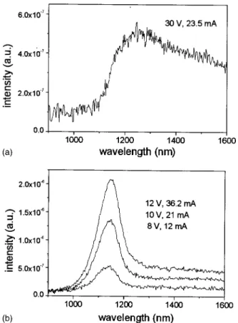
The EL spectrum is discovered to be highly dependent on the surface quality of the Si wafer. To change the surface quality, the polished side of the Si substrate is lapped using sand paper 共No. 400兲. This Si substrate is then put in the setup shown in Fig. 1 with the lapped side facing the ITO surface of the glass. Such a MIS structure also exhibits EL, but has a very broad spectrum. Figure 5共a兲 shows the mea-sured spectrum from 1.0 to 1.7 m, limited by the spectral range of the InGaAs detector. Because lapping creates many surface states with their energies situating in the band gap, electrons in the conduction band could transit to those
sur-FIG. 2. Pressure-dependent I – V characteristics with n-type Si used in the experiment.
FIG. 3. EL spectra from the mechanically pressed MIS structure.
FIG. 4. EL emission strength vs micrometer reading共applied pressure兲.
FIG. 5. EL spectra共a兲 with lapped Si surface. 共b兲 Chemically repolished Si surface.
1809
face states. The measured EL indicates that such transition could be radiative. Such transition also reduces the emission at the band gap energy. As the lapped Si surface is chemi-cally repolished, the EL again has a major emission at the band gap energy, accompanied with relatively small EL at other energies, as shown in Fig. 5共b兲. This indicates that the later chemical polish reduces the surface states, but does not completely remove them. This experiment reveals that the electron–hole radiative recombination and the transition through surface states are competing processes.
The experiment also shows that the simple setup shown in Fig. 1 could be used for surface-quality inspection. Similar to the photoexcitation in photoluminescence experiments, the MIS structure provides the mechanism for up-lifting elec-trons to high-energy states by quantum tunneling. The tun-neled hot electrons then relax to lower energy states by emit-ting photons with corresponding energies. The resulemit-ting EL spectrum could be used for the interpretation of surface in-gredients.
In conclusion, room temperature EL at Si band gap en-ergy is observed from the mechanically pressed ITO/Si con-tact. The I – V curve of the mechanically pressed MIS struc-ture and the EL intensity are pressure-dependent. Increasing pressure simultaneously reduces the I – V rectification char-acteristics and the luminescence. The formation of an air gap between the ITO surface and the Si substrate is crucial for the EL. The role of the air gap is similar to the RTO grown oxide in the MOS structure. The surface quality of Si sub-strate is also experimentally found to have significant influ-ences on the luminescence spectrum, because of the
compe-tition between the band edge emission and the transition through surface states.
This work is supported in part by the National Science Council, Taipei, Taiwan, R.O.C. under Contract Nos. 89-2215-E-002-059 and 89-2112-M-002-076.
1
L. T. Canham, Appl. Phys. Lett. 57, 1046共1990兲.
2N. Koshida and H. Koyama, Appl. Phys. Lett. 60, 347共1992兲.
3S. Lazarouk, P. Jaguiro, S. Katsouba, G. Masini, S. La Monica, G.
Maiello, and F. Ferrari, Appl. Phys. Lett. 68, 2108共1996兲.
4
S. Schuppler, S. L. Friedman, M. A. Marcus, D. L. Adler, Y.-H. Xie, F. M. Ross, Y. J. Chabal, T. D. Harris, L. E. Brus, W. L. Brown, E. E. Chaban, P. F. Szajowski, S. B. Christman, and P. H. Citrin, Phys. Rev. B
52, 4910共1995兲.
5D. B. Geohegan, A. A. Puretzky, G. Duscher, and S. J. Pennycook, Appl.
Phys. Lett. 73, 438共1998兲.
6L. S. Liao, X.-M. Bao, X.-Q. Zheng, N.-S. Li, and N.-B. Min, Appl. Phys.
Lett. 68, 850共1996兲.
7W. Skorupa, R. A. Yankov, I. E. Tyschenko, H. Frob, T. Bohme, and K.
Leo, Appl. Phys. Lett. 68, 2410共1996兲.
8
G. Franzo, F. Priolo, S. Coffa, A. Polman, and A. Carnera, Appl. Phys. Lett. 64, 2235共1994兲.
9M. Matsuoka and S. Tohno, Appl. Phys. Lett. 71, 96共1997兲.
10D. R. Baigent, R. N. Marks, N. C. Greenham, R. H. Friend, S. C. Moratti,
and A. B. Holmes, Appl. Phys. Lett. 65, 2636共1994兲.
11
R. Birkhahn and A. J. Steckl, Appl. Phys. Lett. 73, 1700共1998兲.
12M. Garter, J. Scofield, R. Birkhahn, and A. J. Steckl, Appl. Phys. Lett. 74,
182共1999兲.
13Y. Q. Wang, T. P. Zhao, J. Liu, and G. G. Qin, Appl. Phys. Lett. 74, 3815
共1999兲.
14J. Yuan and D. Haneman, J. Appl. Phys. 86, 2358共1999兲.
15C.-F. Lin, C. W. Liu, M.-J. Chen, M. H. Lee, and I. C. Lin, J. Appl. Phys.
87, 8793共2000兲.
16
C. W. Liu, M.-J. Chen, I. C. Lin, M. H. Lee, and C.-F. Lin, Appl. Phys. Lett. 77, 1111共2000兲.