Physical characteristics and electrical properties of Sr 0.8 Bi 2+x Ta 2 O 9 films on Al 2
O 3 / Si annealed at high temperature
Ban-Chiang Lan, Chih-Yuan Huang, and San-Yuan Chen
Citation: Journal of Applied Physics 94, 6735 (2003); doi: 10.1063/1.1621716
View online: http://dx.doi.org/10.1063/1.1621716
View Table of Contents: http://scitation.aip.org/content/aip/journal/jap/94/10?ver=pdfcov
Published by the AIP Publishing
Articles you may be interested in
Integration of Sr Bi 2 Ta 2 O 9 thin films for high density ferroelectric random access memory
J. Appl. Phys. 100, 051603 (2006); 10.1063/1.2337359
Kelvin probe force microscopy study of SrBi 2 Ta 2 O 9 and PbZr 0.53 Ti 0.47 O 3 thin films for high-density nonvolatile storage devices
Appl. Phys. Lett. 82, 3505 (2003); 10.1063/1.1576916
Bi 3.25 La 0.75 Ti 3 O 12 thin films on ultrathin Al 2 O 3 buffered Si for ferroelectric memory application
Appl. Phys. Lett. 80, 3168 (2002); 10.1063/1.1471937
Effect of annealing temperature on physical and electrical properties of Bi 3.25 La 0.75 Ti 3 O 12 thin films on Al 2 O 3 -buffered Si
Appl. Phys. Lett. 80, 1984 (2002); 10.1063/1.1459115
Electrical characteristics of metal–ferroelectric ( PbZr x Ti 1x O 3 ) –insulator ( Ta 2 O 5 ) –silicon structure for nonvolatile memory applications
J. Vac. Sci. Technol. B 18, 2848 (2000); 10.1116/1.1319698
Physical characteristics and electrical properties of Sr
0.8Bi
2¿xTa
2O
9films
on Al
2O
3Õ
Si annealed at high temperature
Ban-Chiang Lan, Chih-Yuan Huang, and San-Yuan Chena)
Department of Materials Science and Engineering, National Chiao Tung University, Hsinchu, Taiwan, Republic of China
共Received 6 May 2003; accepted 4 September 2003兲
Bismuth-containing layered perovskite Sr0.8Bi2⫹xTa2O9 共SBT兲 thin films with x⫽0 – 0.8 were prepared to investigate annealing temperature effect, especially at high temperature, on physical characteristics and electrical properties of SBT films on Al2O3 共10 nm兲/Si. At 800 °C, the Sr0.8Bi2Ta2⫹xO9/Al2O3/Si exhibits ferroelectric mode and the width of memory window decreases
with the increase of Bi content that is dependent on the effective coercive field. However, at a higher annealing temperature of 900 °C, a larger ferroelectric memory window was obtained for Bi-rich Sr0.8Bi2⫹xTa2O9 (x⫽0.4 or 0.8兲 films compared to SBT film (x⫽0) that should be related to the
reduced leakage current due to the formation of rod-shape grains and amorphous SBT composite layer. The leakage current of Sr0.8Bi2.4Ta2O9/Al2O3/Si annealed at 900 °C is about 1.2 ⫻10⫺9A/cm2 that has two orders of magnitude lower than that of 800 °C-annealed SBT films
measured at⫺100 kV/cm. However, the Sr0.8Bi2Ta2O9 (x⫽0) film on Al2O3/Si capacitor shows
no obvious change with the increase of annealing temperature. © 2003 American Institute of
Physics. 关DOI: 10.1063/1.1621716兴
I. INTRODUCTION
Although the metal/ferroelectric/semiconductors one-transistor memory has been studied for about 40 years,1the progress of this memory is still very slow because of the problems of interface reaction between ferroelectric material and Si.2,3 In order to overcome these problems, an interme-diate layer of SiO2,4 CeO2,5 or Y2O3 共Ref. 6兲 is inserted
between ferroelectric material and Si to form metal/ ferroelectric/insulator/semiconductors structure 共MFIS兲.7,8 However, it was found that the MFIS structure with these buffer layers have large absorption current due to the high density of crystalline defects or carrier traps existing in the interface of Si and buffer layer. Al2O3 has been considered
as the candidate because the Al2O3 is amorphous and good
diffusion barrier with low interface trap density.9 Further-more, taking process integration issues with next generation high performance and low voltage logic technology into ac-count, ultrathin gate dielectrics with large capacitance are required. Recently, we have reported the results of one-transistor共1T兲 ferroelectric metal-oxide-semiconductor field effect transistor 共FeMOSFET兲 memory, using ultrathin Al2O3 with thickness of 40 Å as both gate dielectric and
diffusion barrier due to the high k and excellent diffusion barrier properties.10,11 However, up to now, the discussions of annealing temperature effect on ferroelectric thin films have focused on low processing temperature because high temperature treatment may cause the ferroelectric property deterioration, especially for metal-ferroelectric-metal共MFM兲 structure. It is noticed that although a low temperature an-nealing is required for ferroelectric material used in
one-transistor-one-capacitor ferroelectric random access memory, a high temperature stable ferroelectric is also necessary for the 1T FeMOSFET because of the process integration con-sideration. However, owing to the interdiffusion at the inter-face of ferroelectric/insulator/Si at high annealing tempera-ture, it was commonly recognized that the electrical properties of the MFIS structure would be deteriorated. Therefore, up to now, only little work was focused on the issue of high annealing temperature effect on the electrical properties and structure change. Recently, Lee et al. reported that the memory window of SBT thin films on Si3N4/SiO2/Si capacitor was in the range of 0.75–1.2 V
with annealing temperature from 800 to 900 °C.12Our group has also demonstrated that with increasing annealing tem-perature from 650 to 900 °C, a larger memory window size with a lower leakage current was obtained for BLT/Al2O3/Si capacitor.13 However, no detailed explanation was proposed to elucidate the role of high annealing temperature in the electrical characteristics of MFIS structure. Therefore, the effect of high annealing temperature on electrical properties of SBT-based MFIS structure will be systematically studied in this work.
Furthermore, it is well known that the electrical proper-ties of ferroelectric film are strongly influenced by composi-tion and microstructure change. Previous reports in the lit-erature demonstrated that the bismuth content shows strong influence on the ferroelectric properties of Bi-based MFM structure and that excess Bi is usually required to compen-sate for the loss of Bi due to the high volatility of Bi during processing and Bi diffusion into the bottom electrode during annealing.14,15However, for the Bi-based MFIS structure an-nealed at higher temperature, the effect of excess Bi on the electrical properties and structure change is more important and worthy of investigation. Therefore, in this work, the role
a兲Author to whom correspondence should be addressed; electronic mail:
6735
0021-8979/2003/94(10)/6735/6/$20.00 © 2003 American Institute of Physics
of Bi content in electrical properties of SBT-based MFIS structure will also focused and discussed.
II. EXPERIMENT
4-in. Si p-type wafers were used in this study. After in
situ native oxide desorption, amorphous Al layer was
ther-mally evaporated on wafers. The Al layer was oxidized at a temperature of 400 °C for 2 h to form 10 nm Al2O3 and
finally annealed at 800 °C for 30 min in nitrogen ambient. More detailed fabrication process can be found in our previ-ous works.16The SBT precursors were prepared by metalor-ganic deposition process using strontium 2-ethylhexanotate
关Sr(C8H15O2)2兴, bismuth 2-ethylhexanoate 关Bi(C8H15O2)2兴, tantalum ethoxide 关Ta(OC2H5)5兴 as the
metalorganic precursors. The xylene was used as solvent to mix with metalorganic precursors to form the solution. The solutions with the compositions of Sr0.8Bi2⫹xTa2O9 (x ⫽0 – 0.8) were spin coated on the Al2O3/Si substrate at
4000 rpm for 30 s and then dried on a hot plate at a tempera-ture of about 350 °C. This procedure was repeated for several times to obtain the desired film thickness about 340 nm. The as-deposited films were annealed at different temperatures from 650 to 900 °C for 30 min. After that, the Al electrodes were formed by thermal evaporation. The electrode area of the stacked capacitor is 3.14⫻10⫺4 cm2. The crystal struc-ture of SBT films was detected by MAC Science M18XHF x-ray diffractometer with Cu K␣radiation. The crystal struc-tures of the films were analyzed by using x-ray diffraction
共XRD兲 with Cu K␣ radiation and a Ni filter. The chemical composition of the films was determined using inductively coupled plasma 共ICP兲 mass spectroscopy. Three samples were performed for the ICP analysis and calculated with er-ror deviation of⬃5%. The surface morphology of the films was examined using Hitachi S-4000 scanning electron mi-croscopy 共SEM兲 and the total thickness of SBT films was measured by cross-sectional SEM images. Transmission electron microscopy 共TEM, Philip Technai 20兲 was used to observe the microstructure and analyze the element distribu-tion of the films. The electrical properties were characterized by I – V and C – V measurements using 4156 and HP-4284, respectively.
III. RESULTS AND DISCUSSION A. Crystal phase and microstructure
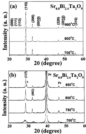
Since the Sr-deficient SBT films have been reported to exhibit more excellent polarization compared to stoichio-metric SBT film,17 the compositions of Sr-deficient Sr0.8Bi2⫹xTa2O9 共SBT兲 with x⫽0 – 0.8 were used in this work. The XRD patterns in Fig. 1共a兲 show that above 700 °C, the 共115兲 diffraction peak of Sr0.8Bi2.4Ta2O9 films becomes sharper and perovskite SBT phase has been fully developed on Al2O3/Si substrates that is probably correlated with
Bi-excess composition and layered perovskite structure of the SBT. Even annealing the Sr0.8Bi2.4Ta2O9 films at 800–
900 °C, the obtained SBT films are polycrystalline and no other second or undesirable pyrochlore phases are detected. Similarly, for the Sr0.8Bi2⫹xTa2O9 films with various Bi
con-tents (x⫽0 – 0.8) annealed at 900 °C, the XRD patterns 共not
shown here兲 illustrate no apparent differences. In contrast, when the SBT was deposited on the Pt/Ti/SiO2/Si substrate,
Fig. 1共b兲 shows that perovskite SBT phase was developed at 700 °C and with increasing annealing temperature up to 850 °C, besides the presence of the perovskite SBT, a small amount of pyrochlore phase was generated especially for the film with x⫽0.18,19
The chemical compositions of Sr0.8Bi2⫹xTa2O9 on
Pt/Ti/SiO2/Si substrate were analyzed by ICP, showing that
after annealed at 800 °C for 0.5 h, the molar ratio of Sr, Bi, and Ta in the film is very close to the composition in the precursor solutions except for a partial loss of Bi and an extra detectable Ti compared to those in precursor solutions. As the Sr0.8Bi2⫹xTa2O9 film was further annealed at 850 °C
for 0.5 h, the Sr/Bi/Ta ratio normalized in Ta⫽2 is approxi-mately to 0.73/1.73/2.0, 0.75/1.97/2.0, and 0.74/2.21/2.11/2.0 for x⫽0, 0.2, and 0.4, respectively. This reveals the occur-rence of Bi loss at such a higher annealing temperature and the importance of excess Bi for the SBT films.
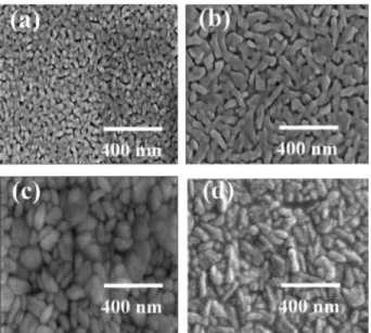
Figure 2 illustrates the typical共FESEM兲 surface images of Sr0.8Bi2⫹xTa2O9 (x⫽0 or 0.4兲 on Al2O3/Si at 800 and 900 °C, respectively. It was observed that the grain size of SBT thin films is strongly dependent on annealing tempera-ture and bismuth content. As shown in Figs. 2共a兲 and 2共b兲 for SBT with x⫽0 and x⫽0.4 films annealed at 800 °C, respec-tively, the grain size is larger for Bi-rich Sr0.8Bi2.4Ta2O9 film
compared to Sr0.8Bi2Ta2O9 film. The microstructure of
Sr0.8Bi2.4Ta2O9 film presents rod-like grains and loose
ma-trix. On the other hand, a dense microstructure consisting of finer and round grains was observed for the Sr0.8Bi2Ta2O9
FIG. 1. XRD patterns of Sr0.8Bi2.4Ta2O9 films on共a兲 Al2O3/Si and 共b兲 Pt/Ti/SiO2/Si as a function of annealing temperature.
6736 J. Appl. Phys., Vol. 94, No. 10, 15 November 2003 Lan, Huang, and Chen
film. As increasing annealing temperature from 800 to 900 °C, a dense microstructure with larger grains was ob-served in Fig. 2共c兲 for the 900 °C-annealed Sr0.8Bi2Ta2O9
thin film. However, for Bi-rich Sr0.8Bi2.4Ta2O9 films shown
in Fig. 2共d兲, a rod-grain or sheet-grain matrix interposed with smaller black areas in between grain boundaries was ob-served, which mostly shows up in the Bi-rich Sr0.8Bi2.4Ta2O9
films at high annealing temperatures.
Figure 3 shows that the cross-sectional TEM image of the Sr0.8Bi2⫹xTa2O9/Al2O3/Si structure annealed at 800–
900 °C in the oxygen ambient. As shown in Figs. 3共a兲 and 3共b兲 for the SBT with x⫽0 and 0.4 films annealed at 800 °C, a sharp interface between Si and Al2O3 was observed. No
apparent difference was seen. With increasing annealing tem-perature up to 900 °C, Fig. 3共c兲 illustrates that a little
diffu-sion envelop共as marked with the arrow兲 was formed at the interface of Al2O3 insulator and Si for the SBT with x⫽0
film. According to EDS analysis共not shown here兲, the reac-tion layer is confirmed to contain the elements of Bi, Al, and Si. On the other hand, for Bi-rich Sr0.8Bi2.4Ta2O9/Al2O3/Si
structure annealed at 900 °C, as shown in Fig. 3共d兲, the Al2O3 layer becomes thinner and the SBT film on Al2O3/Si
was separated into two layers. The top layer is composed of rod-shape SBT grains and the bottom layer becomes amor-phous structure. As revealed by Auger electron spectroscopy
共AES兲 共no shown here兲, the Si has been diffused into Al2O3.
According to our previous study,20 it is suggested that the amorphous structure is probable SBT composite insulator containing Sr, Bi, Ta, Si, and Al.
B.C – V and memory window characteristics
The C – V characteristics of SBT/Al2O3/Si capacitors
were measured at 1 MHz. Figure 4 shows the typical C – V curves and the memory windows of SBT/Al2O3/Si with dif-ferent Bi concentration annealed at 800–900 °C. The bias is swept from ⫺10 to ⫹10 V. The positive memory window value is related to a clockwise hysteresis loop attributed to the ferroelectric mode. It was found that with increasing Bi concentration, the C – V loops were shifted toward right
共positive voltage兲 that is attributed to a little diffusion of Bi
into Si as evidenced from the TEM共Fig. 3兲. The diffusion of Bi into Si causes the enhanced acceptor concentration in the interface and therefore, the charge in the depleted area was increased that cause the shift of threshold voltage to the posi-tive direction. In addition, the decrease in the capacitance
FIG. 2. SEM images of Sr0.8Bi2⫹xTa2O9 films annealed at 800 °C for共a兲
x⫽0, 共b兲 x⫽0.4 and 900 °C for 共c兲 x⫽0, 共d兲 x⫽0.4.
FIG. 3. Cross-sectional TEM images of Sr0.8Bi2⫹xTa2O9/Al2O3/Si
struc-ture annealed at 800 °C for共a兲 x⫽0, 共b兲 x⫽0.4 and 900 °C for 共c兲 x⫽0, 共d兲
x⫽0.4.
FIG. 4. C – V curves of Sr0.8Bi2⫹xTa2O9/Al2O3/Si capacitors as a function of bismuth content at共a兲 800 °C and 共b兲 900 °C.
with increasing the Bi concentration, especially for the MFIS structure annealed at 900 °C, is strongly related to the forma-tion of amorphous SBT shown in Fig. 3共d兲. Figure 5 shows that the SBT films exhibit ferroelectric mode and the width of memory window becomes larger at higher write voltages up to⫾15 V. Above that, the charge injection will be induced into the Al2O3from Si since the electrons severely penetrate into the Al2O3. Therefore, according to the following
rela-tionships, the memory window will be reduced:
Vm⫽2Ec⫺Vci, 共1兲
where Vmis the memory window, 2Ec the effective double
coercive voltage, and Vci the flat-band voltage shift due to
charge injection. The larger memory window of SBT with
x⫽0 compared to that of Bi-rich SBT (x⫽0.4) is primarily
attributed to the decrease in Vci and the increase in 2Ec. As
illustrated in Fig. 6 for the polarization versus electric field hysteresis loops of Pt/SBT/Pt/Ti/SiO2/Si structures, with in-creasing the Bi concentration from x⫽0 to x⫽0.4, the coer-cive field (2Ec) decreases from 145 to 107 kV/cm at the applied voltage of 6 V, indicating that the SBT with x⫽0 shows a larger memory window than that with x⫽0.4 on the same Al2O3/Si structure because the former has a larger
coercive field than the latter based on Eq. 共1兲.
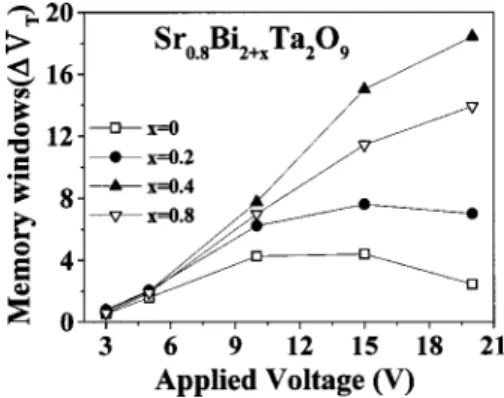
As the Sr0.8Bi2⫹xTa2O9/Al2O3/Si was annealed at
900 °C, Fig. 7 demonstrates that the memory window in-creases with the applied voltage, and a saturated memory
window of 4 –7 V was attained for the SBT with x⫽0 and 0.2 films. In sharp contrast, for the Bi-rich SBT films (x
⫽0.4 and 0.8兲, the memory window values become larger at
higher applied voltages even up to ⫾20 V. A large memory window of 18 V was obtained for the 900 °C-annealed samples at the applied voltage of 20 V and this should be the largest ferroelectric memory window reported so far. Al-though the SiO2 was probably formed, from the
cross-sectional TEM image 共not shown here兲, no obvious SiO2
interface layer was detected even in the higher magnification. Therefore, the effect of SiO2on the effective field applied on
the SBT can be neglected because it is too thin 共⬍1 nm兲 to be detected. The enhancement of memory window can be elucidated by the electric field distribution between the SBT and Al2O3 as follows:
Ef⫽
冉
i fdi⫹idf冊
VG, 共2兲
where E,, and d are the effective applied to a capacitor, the dielectric constant, and the thickness, respectively. The sub-scripts of f and i stand for the ferroelectric and insulator, respectively, and VG is the applied gate voltage. As one can
see the cross-sectional TEM of Bi-rich Sr0.8Bi2.4Ta2O9/Al2O3/Si in Fig. 3共d兲, the original SBT was
separated into two layers consisting of high dielectric (
⫽200– 250) perovskite SBT and low dielectric constant
amorphous SBT structure. Therefore, the dielectric constant of the overall Bi-rich SBT can be decreased and more ap-plied voltage is distributed over the SBT film compared to SBT with x⫽0 film. Furthermore, owing to the formation of amorphous SBT structure that is similar to the insulator, the Sr0.8Bi2⫹xTa2O9/Al2O3/Si can be applied under a higher voltage without dielectric breakdown. Therefore, a larger memory window can be obtained for the Sr0.8Bi2⫹xTa2O9 (x⫽0.4 and 0.8兲/Al2O3/Si.
The above results apparently reveal the importance of Bi content on memory characteristics of the SBT/Al2O3/Si
structure. In addition, as the SBT films were annealed at such a higher temperature, the Bi loss from either evaporation or diffusion would occur. As shown in the ICP results for SBT films on Pt/Ti/SiO2/Si substrates, the Bi concentration in the
Bi-rich SBT (x⫽0.4) films is close to 2 (x⫽0). According to our results in Fig. 6 and the report of Watanabe et al.21
FIG. 5. Relationship between memory window and applied voltage for Sr0.8Bi2⫹xTa2O9/Al2O3/Si capacitors annealed at 800 °C.
FIG. 6. P – E hysteresis loops of Sr0.8Bi2⫹xTa2O9 films with various bis-muth contents on Pt/Ti/SiO2/Si annealed at 800 °C for 0.5 h under an ap-plied voltage of 6 V.
FIG. 7. Relationship between memory window and applied voltage for Sr0.8Bi2⫹xTa2O9/Al2O3/Si capacitors annealed at 900 °C.
6738 J. Appl. Phys., Vol. 94, No. 10, 15 November 2003 Lan, Huang, and Chen
that the stoichiometric SBT film shows a larger coercive field compared to Bi-less and Bi-rich SBT films. Therefore, at 900 °C, a maximum memory window appears at the SBT film with x⫽0.4. This further demonstrates that the memory window is dominated by not only the annealing temperature but also the bismuth content in the SBT films.
C. Leakage current
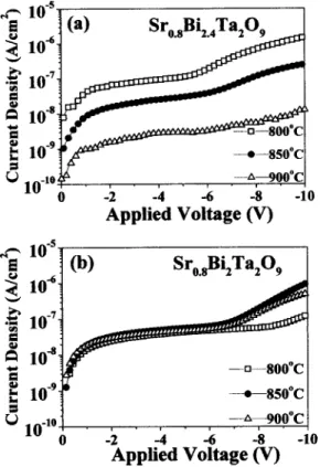
We have also investigated the current–voltage character-istics because the leakage current is one of the most important properties for memory capacitor. Figure 8 illus-trates J – V curves of Sr0.8Bi2⫹xTa2O9/Al2O3/Si capacitors
annealed at different temperatures. As shown in Fig. 8共a兲, the leakage current density of Sr0.8Bi2.4Ta2O9/Al2O3/Si/Al2O3/Si annealed at 800 °C is
1.7⫻10⫺7A/cm2 at ⫺100 kV/cm and it increases at high voltages. On the other hand, for the samples annealed at 900 °C, the leakage current (1.2⫻10⫺9 A/cm2) reduces ⬃2 orders of magnitude at⫺100 kV/cm. In addition, no dielec-tric breakdown up to ⫺10 V also implies that the Bi-rich SBT film annealed at high temperatures has better dielectric integrity than that annealed at 800 °C. This smaller leakage current and larger breakdown voltage for Bi-rich SBT films annealed at 900 °C may be related to the microstructure of rod-shape grains and the formation of insulator amorphous SBT that makes the leakage current lower. Similar trend was also observed in our previous research for ferroelectric BLT thin films on Al2O3/Si.13 On the other hand, for
Sr0.8Bi2Ta2O9 thin film annealed at 800 °C 关Fig. 8共b兲兴, a
lower leakage current was obtained as compared to Sr0.8Bi2.4Ta2O9 film that is probably due to the diffusion of
Bi or the formation of highly conductive Bi2O3 as revealed
by Shimakawa et al.14 At 900 °C, although the enhanced densification in the SBT films can reduce the leakage current, the increased grain size probably leads to the increase of leakage current. Therefore, with an increase of annealing temperature, no obvious change in the leakage current of Fig. 8共b兲 was observed for the SBT (x⫽0) film. However, the leakage current of the SBT (x⫽0) film at 900 °C is still higher than that of Bi-rich SBT (x⫽0.4) film based on the Sr0.8Bi2⫹xTa2O9/Al2O3/Si structure.
IV. CONCLUSION
In conclusion, we have studied the annealing tempera-ture dependent characteristics of Sr0.8Bi2⫹xTa2O9/Al2O3/Si.
At 800 °C, the Sr0.8Bi2⫹xTa2O9/Al2O3/Si exhibits
ferroelec-tric mode. With increasing annealing temperature up to 900 °C, it was found that Bi-rich SBT(x⫽0.4)/Al2O3/Si
presents a larger memory window compared to SBT film (x⫽0) that should be related to the reduced leakage current due to the formation of rod-shape grains and amorphous SBT layer. The leakage current of Sr0.8Bi2.4Ta2O9/Al2O3/Si
an-nealed at 900 °C is about 1.2⫻10⫺9 A/cm2 at 100 kV/cm and reduced by two orders of magnitude lower than that annealed at 800 °C. All the results in this study demonstrate that the high annealing temperature makes the stack gate SBT/Al2O3/Si process compatible with current VLSI tech-nology.
ACKNOWLEDGMENT
This work has been supported by the National Science Council Contract No. NSC-91-2215-E-009-051 of Taiwan.
1J. L. Moll and Y. Tarui, IEEE Trans. Electron Devices ED-10, 338共1963兲. 2Y. Shichi, S. Tanimoto, T. Goto, K. Kuroiwa, and Y. Tarui, Jpn. J. Appl.
Phys., Part 1 33, 5172共1994兲.
3S. Y. Wu, Ferroelectrics 11, 379共1976兲.
4T. Hirai, K. Teramoto, T. Nishi, T. Goto, and Y. Tarui, Jpn. J. Appl. Phys.,
Part 1 33, 5219共1994兲.
5
E. Tokumitsu, K. Itani, B. K. Moon, and H. Ishiwara, Jpn. J. Appl. Phys., Part 1 34, 5202共1995兲.
6T. Kanashima and M. Okuyama, Jpn. J. Appl. Phys., Part 1 38, 2044
共1999兲.
7Y. T. Kim and D. S. Shin, Appl. Phys. Lett. 71, 3507共1997兲. 8
Y. Matsui, M. Okuyama, M. Noda, and Y. Hamakawa, Appl. Phys. A: Solids Surf. 28, 61共1982兲.
9X. H. Liu, Z. G. Liu, and J. M. Liu, Appl. Phys. A: Mater. Sci. Process. 73,
331共2001兲.
10S. Y. Chen, C. L. Sun, S. B. Chen, and A. Chin, Appl. Phys. Lett. 80, 3168
共2002兲.
11C. L. Sun, J. J. Hsu, S. Y. Chen, and A. Chin, J. Electrochem. Soc. 150,
G187共2003兲.
12W. J. Lee, C. H. Shin, C. R. Cho, J. S. Lyu, B. W. Kim, B. G. Yu, and K.
I. Cho, Jpn. J. Appl. Phys., Part 1 38, 2039共1999兲.
13
C. L. Sun, S. Y. Chen, S. B. Chen, and A. Chen, Appl. Phys. Lett. 80, 1984
共2002兲.
14Y. Shimakawa and Y. Kubo, Appl. Phys. Lett. 75, 2839共1999兲. 15Y. T. Kim, D. S. Shin, Y. K. Park, and I. H. Choi, J. Appl. Phys. 86, 3387
共1999兲.
16M. Y. Yang, S. B. Chen, A. Chin, C. L. Sun, B. C. Lan, and S. Y. Chen,
Tech. Dig.-Int. Electron Devices Meet. 2001, 36_03.1.
FIG. 8. Dependence of annealing temperatures on J – V characteristics of共a兲 Sr0.8Bi2.4Ta2O9and共b兲 Sr0.8Bi2Ta2O9on Al2O3/Si.
17T. Noguchi, T. Hase, and Y. Miyasaka, Jpn. J. Appl. Phys., Part 1 35, 4900
共1996兲.
18M. A. Rodriguez, T. J. Boyle, B. A. Hernandez, C. D. Buchheit, and M. O.
Eatough, J. Mater. Res. 11, 2282共1996兲.
19C.-H. Lu and B.-K. Fang, J. Mater. Res. 12, 2104共1997兲. 20
C. L. Sun and S. Y. Chen, J. Electrochem. Soc. 150, C600共2003兲.
21H. Watanabe, T. Mihara, H. Yoshmori, and C. A. Paz de Araujo, Jpn. J.
Appl. Phys., Part 1 34, 5240共1995兲.
6740 J. Appl. Phys., Vol. 94, No. 10, 15 November 2003 Lan, Huang, and Chen