Metal drift induced electrical instability of porous low dielectric constant film
Kuo-Lung Fang and Bing-Yue Tsui
Citation: Journal of Applied Physics 93, 5546 (2003); doi: 10.1063/1.1563292 View online: http://dx.doi.org/10.1063/1.1563292
View Table of Contents: http://scitation.aip.org/content/aip/journal/jap/93/9?ver=pdfcov Published by the AIP Publishing
Articles you may be interested in
Dielectric/metal sidewall diffusion barrier for Cu/porous ultralow-k interconnect technology Appl. Phys. Lett. 84, 2442 (2004); 10.1063/1.1695205
Low dielectric constant materials for microelectronics J. Appl. Phys. 93, 8793 (2003); 10.1063/1.1567460
Direct patterning of photosensitive low-dielectric-constant films using electron-beam lithography Appl. Phys. Lett. 78, 2557 (2001); 10.1063/1.1360777
Comparison of ultrathin CoTiO 3 and NiTiO 3 high-k gate dielectrics J. Appl. Phys. 89, 3447 (2001); 10.1063/1.1347405
Low dielectric constant film formation by oxygen-radical polymerization of laser-evaporated siloxane J. Vac. Sci. Technol. B 15, 746 (1997); 10.1116/1.589380
Metal drift induced electrical instability of porous low dielectric
constant film
Kuo-Lung Fanga) and Bing-Yue Tsui
Department of Electronics Engineering and Institute of Electronics, National Chiao-Tung University, Hsinchu 300, Taiwan, Republic of China
共Received 26 August 2002; accepted 3 February 2003兲
Nano-porous carbon doped oxide 共CDO兲 is one of the potential low dielectric constant 共low-k兲 materials that can achieve a dielectric constant as low as 2.2 and is expected to be suitable for the next generation multilevel interconnection. However, the electrical stability of CDO in contact with metal has not been addressed. In this work, metal ions’ drift into nano-porous CDO is investigated. It is observed that both the Al and Cu ions can be driven into porous CDO film easily by applying electric field or thermal treatment. This results in a severe flat band voltage shift of the metal/CDO/ Si capacitor structure. It is hypothesized that the lacking formation of self-limited aluminum oxide between Al and CDO film make Al ions drift into CDO. The adhesion of Al and Cu to CDO is also very poor. A physical model, combining weak dielectric polarization and metal ions drift, was proposed to explain the observed electrical instability. The inconsistent results regarding the Al/ porous low-k/Si structure reported in the previous literatures can also be explained with this proposed model. Fortunately, TaN, as a common diffusion barrier material for Cu interconnect structure, is proved to have good adhesion to CDO. Negligible metal ions would drift in CDO during electrical stress. It is concluded that with a suitable diffusion barrier, such as TaN, CDO is still a very promising material for next generation Cu-interconnect technology. © 2003 American
Institute of Physics. 关DOI: 10.1063/1.1563292兴
INTRODUCTION
As in ultra-large scale integrated circuits generations, the implementation of copper-interconnect structures with low-k materials is the only solution to reduce overall signal delay in several technology nodes in the future.1,2Since Cu is the metal with the second lowest resistivity, adopting lower di-electric constant materials is the only method to further im-prove the resistance-capacitance time delay. According to the
International Technology Roadmap for Semiconductor
pub-lished in 2001, the bulk dielectric constant of low-k material must be reduced to lower than 2.4 by 2006.3 In the past 10 years, lots of varieties of low-k materials are being developed with different chemical composition. By changing film po-larity, changing chemical bonds, or inserting lower weighted molecular atoms, one can intrinsically reduce the k value to about 2.7.4 In order to further reduce dielectric constant, there is an unavoidable trend of developing porous type low-k films. With the free air volume pore structures in bulk low-k film, a very low dielectric constant could be reached.5– 8
Among the nano-porous low-k materials, nano-porous carbon-doped oxide 共CDO兲 is one of the most promising porous low-k materials to date.9–12CDO could be deposited in a plasma-enhanced chemical vapor deposition 共PECVD兲 system with additional curing process to produce a stable state. A very low dielectric constant of 2.2 has been achieved. It is reported that CDO exhibits a very low leakage current 共⬍1 nA/cm2 at 2.5 MV/cm兲, a very high thermal
stability 共⬎600 °C in N2 ambient兲, and strong electrical strength 共⬎5 MV/cm at 200 °C兲. It has been demonstrated successfully integrating with Cu in a full dual damascene structure.13 The above information indicates that CDO is a very potential material for next generation intermetal dielec-tric 共IMD兲.14 But, not many electrical properties have been discussed in previous literatures.
On the other hand, Cu shows many advantages in com-parison with Al15but also new problems appear. The drift of Cu ions into IMD is one of the most important issues that should be carefully studied. Cu mobile ions in IMD would always induce defect traps and cause reliability issues and even degrade lifetime of the devices. To understand the Cu drift in IMD is meaningful for not only academic interest but also practical application. A bias temperature stress 共BTS兲 test on a Cu/Low-k film/Si sandwiched capacitor structure is always employed to study Cu drift behavior in low-k thin
a兲Electronic mail: [email protected]
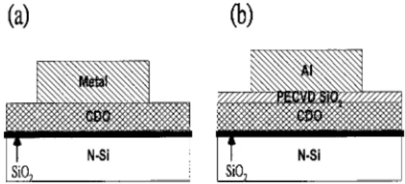
FIG. 1. Schematic drawing of the MIS structures used in this work:共a兲 Metal-MIS 共Al-MIS, Cu-MIS and TaN-MIS兲: Metal/CDO(200 nm兲/ SiO2(10 nm兲/Si. 共b兲 Al-MIS-2: Al/PECVD SiO2(30 nm兲/CDO(200 nm兲/
SiO2(10 nm兲/Si.
5546
0021-8979/2003/93(9)/5546/5/$20.00 © 2003 American Institute of Physics
film. Aluminum, being a very stable interconnection metal, was used as a reference to distinguish Cu drift and the other issues. Recently, some unusual phenomenon happened to these recently developed porous low-k materials. Al gated capacitor structures exhibit an unaccustomed Vfb shift after positive electric-field stress. Quite different explanations were proposed in those literatures.16 –18All of these proposed models: interface-related charges, instabilities occurred when Al came in contact with low-k film, charges injects and trapped inside low-k film, and Al ions drift in low-k, are not consistent with each other. Besides, all these models were proposed on the basis of electrical analysis data without any material analysis evidences.
The significance of studying metal drift in low-k material is manifold. At first, integration scheme is dependent on metal drift in low-k material. Second, interconnect reliability is strongly affected by metal ions in low-k dielectric. Third, to monitor Cu contamination, metal drift behavior must be known in advance. Therefore, we investigated the drift of metal ions in a nano-porous low-k film and studied the metal ions induced electrical instability in this work. A metal ions drift model in porous CDO is also proposed.
EXPERIMENTAL PROCEDURE
A simple metal-insulator-silicon 共MIS兲 capacitor struc-ture was used in this work. The starting material was 共100兲-oriented n-type silicon wafer. A 10 nm thick oxide was ther-mally grown before CDO deposition to minimize the insulator/silicon interface state density. CDO film was depos-ited in a plasma-enhanced chemical vapor deposition 共PECVD兲 system using Trikon Technologies Planar 300 PECVD system named Orion™. The total thickness of CDO
is 200 nm. Various metals, Al, Cu, and TaN were deposited through a metal mask to form gate electrodes. Samples are referred as Al-MIS, Cu-MIS, and TaN-MIS. Al was depos-ited in a thermal evaporation system while Cu and TaN were deposited in a sputtering deposition system. The structure of the MIS capacitor is then formed metal/CDO(200 nm兲/ SiO2(10 nm兲/Si. A thin Si3N4 layer of 30 nm thickness was deposited to passivate the MIS structure. Al deposition at backside and 400 °C annealing in N2 ambient for 30 min were performed before electrical measurement. Some Al-gate capacitors 共referred to as Al-MIS-2 sample兲 with a 30 nm thick PECVD oxide on CDO were also fabricated. Figure 1 shows the schematic drawings of the two sample struc-tures. Unpatterned metal/CDO/SiO2/Si and Al/SiO2/Si structures were also prepared for nonelectrical analysis.
Capacitance-voltage (C – V) electrical measurements were performed to evaluate the CDO film stability using a FIG. 2. Capacitance-voltage curves of Al-MIS sample measured from
inver-sion mode to accumulation mode共FVS兲 and from accumulation mode to inversion mode共RVS兲.
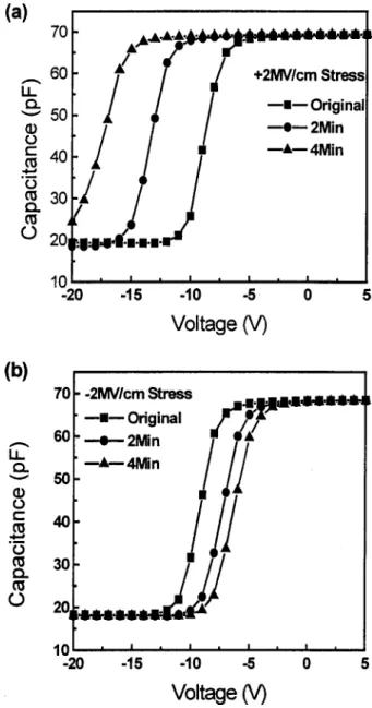
FIG. 3. Capacitance-voltage curves of Al-MIS samples after electrical stress at共a兲 ⫹2 MV/cm and 共b兲 ⫺2 MV/cm for various time periods at room temperature.
TABLE I. Flat band voltage shift of MIS structures with various metal gate materials after BTS test at 0.6 MV/cm for 30 min.
Temperature共°C兲 Al共V兲 Cu共V兲 TaN共V兲 Al-MIS-2共V兲
30 °C ⫺7.48 ⫺3.2 ⫺2.74 ⫺0.07
150 °C ⬍⫺40 ⬃⫺40 ⫺9.6 ⫺5.12
5547
J. Appl. Phys., Vol. 93, No. 9, 1 May 2003 K.-L. Fang and B.-Y. Tsui
precision impedance meter of model Agilent 4284A. A bias-temperature stress test on MIS samples was performed at various temperatures and electric fields to evaluate the be-havior of metal ion drift in CDO film. Flat band voltages before and after BTS were extracted from high frequency 共100 KHz兲 C – V characteristic with voltage sweep either from inversion mode to accumulation mode共forward voltage sweep, FVS兲 or from accumulation mode to inversion mode 共reverse voltage sweep, RVS兲. Secondary ion mass spectros-copy共SIMS兲 analysis was performed on MIS capacitors be-fore and after the BTS test to determine the depth distribu-tion of metal in CDO film.
RESULT AND DISCUSSION
Table I summarizes the value of Vfb shift of Al-MIS, Cu-MIS, and TaN-MIS samples after the BTS test at 0.6 MV/cm for 30 min. The magnitudes of Vfbshift of the MIS capacitors are Al-MIS, Cu-MIS, and TaN-MIS in the se-quence from high to low. The lowest Vfbshift of TaN-MIS sample is as expected because TaN is stable and acts as very good diffusion barrier of metals. The negative Vfbshift of the Cu-MIS sample is always explained by Cu drift in dielectric.
What is unexpected is that the magnitude of the Vfbshift of Al-MIS sample is larger than that of the Cu-MIS sample.
By repeating the C – V measurement on the Al-MIS ca-pacitor from inversion mode to accumulation mode 共FVS兲 and then from accumulation mode to inversion mode共RVS兲, the C – V shift with respect to the original C – V curve was found. As shown in Fig. 2, the C – V curve shifts toward the right-hand side under FVS, while it shifts toward the left-hand side under RVS. The shifts under FVS and RVS are asymmetric and a net left shift was observed. Figures 3共a兲 and 3共b兲 show the C – V curves of the Al-MIS sample after continuous electrical stress at ⫹2 and ⫺2 MV/cm, respec-tively. It is was also found that the magnitude of the Vfbshift under positive electric-field stress is larger than that under negative electric-field stress. Because of the asymmetric shift, the C – V instability cannot be simply explained with the dielectric polarization19 and further investigations were made to find out the root cause of instability.
It is well known that Al is quite stable in contacting with SiO2 because a very thin self-limiting Al2O3 forms between Al and SiO2 and acts as a good diffusion barrier.
16 –17 The negligible Vfbshift of the Al-MIS-2 sample at 30 °C indicates that CDO itself is electrically stable at room temperature. Therefore, the ⫺7.48 V Vfbshift of the Al-MIS sample im-plies that Al ions can be driven into CDO at room tempera-ture. It is well known that Al ions do not enter SiO2 under the BTS test; the Vfbshift of Al-MIS-2 capacitor after BTS at 150 °C would be attributed to the intrinsic instability of CDO, i.e., dielectric polarization.19 But as Al contacts with the CDO film directly, the Vfbshift is well beyond ⫺40 V
共see Table I兲. The magnitude of the Vfbshift of the Al-MIS
FIG. 4. SIMS depth profiles of共a兲 Al-MIS sample and 共b兲 Cu-MIS sample before and after the BTS test at⫹1 MV/cm and 200 °C for 60 min.
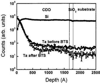
FIG. 5. SIMS depth profiles of TaN-MIS sample before and after the BTS test at⫹1 MV/cm and 200 °C for 60 min.
TABLE II. Results of pull-stud adhesion test of different metal/CDO inter-face and Al/SiO2interface.
Al/CDO Cu/CDO TaN/CDO Al/SiO2
Average共MPa兲 16.82 19.1 51.92 47.02
Standard deviation共MPa兲 5.62 9.53 11.46 7.37
sample excludes the CDO instability effect 关Vfb(Al-MIS) subtracts Vfb(Al-MIS-2)] is still very large, and thus the possible cause of this severe instability might be Al ions drifting into CDO film. Figure 4共a兲 compares the distribution of Al atoms in CDO before and after the BTS test at 150 °C. It is apparent that Al ions were driven throughout the whole CDO. Figure 4共b兲 shows that, similar to Al, Cu can be easily driven into CDO with the same BTS test. It is well known that Cu is a fast diffuser in most of the dielectric materials. This observation confirms that the Vfbshift of the Cu-MIS sample is due to Cu drift.
TaN is known to be inert in comparison with Al and Cu and is used as a barrier metal between metal interconnect and dielectric thin film. It is not expected to inject ions into di-electric di-electrical stress. The Ta profiles of the TaN-MIS sample are almost identical before and after BTS at 150 °C as shown in Fig. 5. This result implies that the Vfbshift of the TaN-MIS capacitor listed in Table I is not due to metal ions. Actually, a slight distortion of C – V curve was observed on the BTS tested TaN-MIS sample. The slightly larger Vfbshift of the TaN-MIS sample than that of the Al-MIS-2 sample is thus attributed to the dielectric polarization together with process damage during TaN deposition.
The apparent Al diffusion into CDO implies the lack of Al2O3 formation at the Al/CDO interface.
16 –17
Table II lists the results of pull-stud adhesion test of different metal/CDO and Al/SiO2 interfaces. As expected, Al shows good adhe-sion to oxide dielectric thin film, while both Al and Cu show very poor adhesion to CDO. The poor adhesion between Al and CDO is another side evidence that no interfacial reaction
between Al and CDO occurs. Fortunately, TaN, as a common diffusion barrier material for Cu, is proved to have good adhesion to CDO.
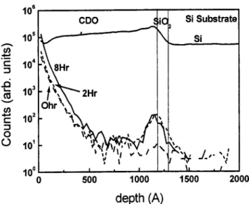
The lacking formation of self-limited aluminum oxide between Al and CDO film allow Al ions to be driven into CDO film. Besides, the porous structure of CDO film con-tains nano-pores. Al ions can easily be driven into a deep portion of CDO along with these pores. Table III lists the Vfb values of just fabricated Al-MIS samples after annealing in N2ambient at 400 °C for various time periods. The Vfbshifts toward negative voltage with the increase of annealing time. This result means that more Al ions diffuse into CDO film under long-time thermal anneal. Figure 6 shows the Al depth profile of Al-MIS sample after annealing. The Al metal gate had been removed before SIMS analysis. It is confirmed that Al atoms did diffuse into CDO film after 8 h annealing. Besides, Al atoms piled up at CDO/SiO2 interface and can-not diffuse though the SiO2 layer. This phenomenon is con-sistent with our hypothesis that the lacking of alumni oxide layer between Al and CDO leads to the drift and/or diffusion of Al into CDO.
Now the electrical instability of the metal/CDO/Si struc-ture can be understood with the model proposed in Fig. 7. Weak polarization occurs under electric field at high-temperature stress for all Metal-MIS capacitor and this is what we have named as CDO intrinsic instability that causes
Vfbto shift left. As the gate is positively biased, some kinds of metal ions 共Al or Cu兲 may be driven from the gate into CDO and move quickly along nano-pore structures into deeper bulk dielectric. This phenomenon would cause metal/ CDO/Si structure to be electrically unstable.
CONCLUSIONS
Our investigation discovered that the lacking formation of Al2O3 interfacial layer caused Al ions to migrate into
FIG. 6. SIMS depth profiles of Al-MIS samples after annealing at 400 °C for various time periods.
TABLE III. Flat band voltage shift of Al-MIS sample after annealing at 400 °C for various time periods.
CDO 0 h 2 h 8 h
Average共V兲 ⫺1.59 ⫺2.73 ⫺3.52
Standard deviation共V兲 0.24 0.31 0.33
FIG. 7. Schematic illustration of the proposed model to explain the electri-cal instability of Metal/CDO system.
5549
J. Appl. Phys., Vol. 93, No. 9, 1 May 2003 K.-L. Fang and B.-Y. Tsui
CDO film and the CDO porous structure would enhance metal ions movement in it. An electrical instability model combining weak dielectric polarization and metal ions drift was proposed to explain the instability observed on the po-rous CDO film. This model may be applied to the instability phenomenon observed on the other porous low-k materials where inconsistent explanations were proposed in previous literatures.
Although both Al and Cu ions can be driven into CDO under electrical stress, no metal ions are observed in CDO with TaN gate. Furthermore, TaN shows excellent adhesion to CDO. Combining with those good properties reported pre-viously, CDO is still a very promising material for next gen-eration Cu-interconnect technology.
ACKNOWLEDGMENTS
The authors would like to express their deep gratitude to Dr. S. D. Lee for SIMS analysis. This work is partially sup-ported by the National Science Council, R.O.C, under Con-tract No. NSC-90-2215E-009-064. Samples were processed in National Nano Device Laboratories, R.O.C.
1Ronald J. Gutmann, IEEE Trans. Microwave Theory Tech. 47, 667共1999兲. 2Nobuyoshi Awaya, Hiroshi Inokawa, Eiichi Yamamoto, Yukio Okazaki,
Masayasu Miyake, Yoshinobu Arita, and Toshio Kobayashi, IEEE Trans. Electron Devices 43, 1206共1996兲.
3The National Technology Roadmap for Semiconductors共Semiconductor
Industry Association, San Jose, California, 2001兲.
4J. H. Golden, C. J. Hawker, and P. S. Ho, Designing Porous Low-k
Di-electrics共Semiconductor International, 2001兲.
5N. Aoi, Jpn. J. Appl. Phys., Part 1 36, 1355共1997兲.
6W. Wu, W. E. Wallace, E. K. Lin, G. W. Lynn, C. J. Glinka, E. T. Ryan,
and H. M. Ho, J. Appl. Phys. 82, 1193共2000兲.
7M. H. Jo, H. H. Park, D. J. Kim, S. H. Hyun, S. Y. Choi, and J. T. Paik, J.
Appl. Phys. 87, 1299共1997兲.
8
D. R. Denison, J. C. Barbour, and J. H. Burkart, J. Vac. Sci. Technol. A 14, 1124共1996兲.
9M. Tada, Y. Harada, K. Hijioka, H. Ohtake, T. Takeuchi, S. Saito, T.
Onodera, M. Hiroi, N. Furutake, and Y. Hayashi, IEEE International
In-terconnect Technology Conference共2002兲, p. 12.
10
J. C. Lin, R. Augur, S. L. Shue, C. H. Yu, M. S. Liang, A. Vijayendran, T. Suwwan de Felipe, and M. Danek, IEEE International Interconnect
Tech-nology Conference共2002兲, p. 21.
11H. J. Lee, Y. H. Kim, J. Y. Kim, E. K. Lin, B. J. Bauer, W. I. Wu, and H.
J. Kim, IEEE International Interconnect Technology Conference共2002兲, p. 54.
12C. Waldfried, Q. Han, O. Escorica, A. Margolis, R. Albano, and I. Berry,
IEEE International Interconnect Technology Conference共2002兲, p. 226.
13K. Buchanan, K. Beekmann, K. Giles, J-C. Yeoh, and H. Donohue,
Pro-ceeding of Advanced Metallization Conference共2001兲, p. 73.
14
K.-L. Fang, B.-Y. Tsui, C.-C. Yang, M.-C. Chen, S.-D. Lee, K. Beekmann, T. Wilby, K. Giles, and S. Ishaq, IEEE International Interconnect
Tech-nology Conference共2002兲, p. 60.
15S. P. Murarka and S. W. Hymes, Crit. Rev. Solid State Mater. Sci. 20, 87
共1995兲.
16A. L. S. Loke, J. T. Wetzel, P. H. Townsend, T. Tanabe, R. N. Vrtis, M. P.
Zussman, D. Kumar, C. Ryu, and S. S. Wang, IEEE Trans. Electron De-vices 46, 2178共1999兲.
17A. Mallikarjunan, S. P. Murarka, and T. M. Lu, Appl. Phys. Lett. 79, 1855
共2001兲.
18A. Jain, S. Rogojevic, S. Ponoth, N. Agarwal, I. Matthew, W. N. Gill, P.
Persans, M. Tomozawa, and J. L. Plawsky, E. Simonyi, Thin Solid Films
398–399, 513共2001兲.
19
B. Y. Tsui, K. L. Fang, and S. D. Lee, IEEE Trans. Electron Devices 48, 2375共2001兲.