Microstructures and dielectric properties of PZT thick films prepared by
aerosol plasma deposition with microwave annealing
C.M. Huang
a, S.F. Wang
a, C.J. Peng
b, J. Shieh
c,∗, C.S. Chang
b, T.S. Lin
baDepartment of Materials and Minerals Engineering, National Taipei University of Technology, 1 Chung-Hsiao East Road, Sec. 3, Taipei 106, Taiwan bMaterials Research Laboratory, Industrial Technology Research Institute, 195 Chung-Hsing Road, Sec. 4, Hsinchu 310, Taiwan
cDepartment of Materials Science and Engineering, National Taiwan University, 1 Roosevelt Road, Sec. 4, Taipei 106, Taiwan Received 20 April 2006; received in revised form 21 June 2006; accepted 24 June 2006
Abstract
Lead zirconate titanate (PZT) thick films have been successfully grown on Pt/Ti-coated (1 0 0) Si substrates by a novel aerosol plasma deposition (APD) method at room temperature. The dielectric constant (K) and loss tangent (tanδ) of the as-deposited film measured at 100 kHz are 223 and 0.034, respectively. The dielectric properties of the film are improved considerably by subsequent microwave annealing: K = 745 and tanδ = 0.024 are achieved for films which are microwave-annealed at 600 W for 3 min, and K = 1049, tanδ = 0.027, and remanent polarization (Pr) = 32C cm−2 for films annealed at 800 W for 3 min. These values are comparable to those of PZT films grown by conventional deposition methods with high substrate and/or post-annealing temperatures.
© 2006 Elsevier B.V. All rights reserved.
Keywords: PZT; Thick films; Aerosol plasma deposition; Microwave annealing
1. Introduction
Lead zirconium titanate (PZT)-based thin and thick films are promising candidates for electronic, sensing, micro-actuating, microelectronic mechanical system (MEMS), and non-volatile memory applications due to their superior ferroelec-tric and piezoelecferroelec-tric characteristics. Common deposition pro-cesses for PZT films are RF magnetron sputtering, metal organic chemical vapor deposition (MOCVD), metal organic decompo-sition (MOD), and sol–gel, etc.[1–3]. PZT films produced by most deposition processes require post-annealing at relatively high temperatures (>550◦C) in order to attain preferable crystal orientations and dielectric and mechanical properties. However, high annealing temperatures might cause problems such as inter-diffusion between layers, large residual stresses, compositional changes, and lead loss, etc., which hinder the wider integration of PZT films into various MEMS fabrications[4–6]. In order to eliminate or minimize these problems, low temperature prepa-ration of PZT films at both the deposition and post-annealing stages is desirable. In the present study, low temperature
depo-∗Corresponding author. Tel.: +886 2 33665287; fax: +886 2 23634562.
E-mail address:[email protected](J. Shieh).
sition of PZT thick films on silicon substrates (with platinum electrodes) by a novel aerosol plasma deposition (APD) method, combined with subsequent microwave annealing, is described. The deposition phase of APD is carried out at room tempera-ture, while the temperature during annealing ranges up to 420◦C, depending on the microwave power. The design and operating principles of APD reported in the present study are developed based on the concept of aerosol film deposition originally pro-posed by Akedo and co-workers[7–9].
2. Experimental procedure
Sr- and Nb-doped PZT powder, (Pb0.95Sr0.05
)-((Zr0.52Ti0.48)0.98Nb0.02)O3, is chosen for the aerosol
deposi-tion. The powder is prepared by solid-state reaction where PbO, SrCO3, ZrO2, TiO2and Nb2O5are mixed, ball-milled for 18 h,
and then calcined at 900◦C for 2 h. The calcined powder has a grain size of 200–500 nm.Fig. 1shows the SEM image of the powder. The APD apparatus is schematically shown inFig. 2; construction details of this apparatus have been previously presented [10]. PZT thick films are deposited by APD on Pt/Ti-coated (1 0 0) Si substrates, which are maintained at room temperature throughout the deposition process. The aerosol is formed by introducing a carrier gas of Ar/O2 mixture into a 0921-5107/$ – see front matter © 2006 Elsevier B.V. All rights reserved.
Fig. 1. SEM micrograph of PZT powder prepared by solid-state reaction.
Fig. 2. Schematic of the APD apparatus.
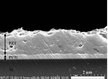
glass jar containing the PZT powder. The PZT aerosol then interacts with a microwave-driven plasma before impacting onto the substrate under vacuum. The deposition parameters adopted in the present study are listed in Table 1. To obtain a uniform film thickness across a large area, the substrate is placed on an XY stage and bi-directionally scanned at a speed of 1.5 mm/step, using a zigzag pattern.Fig. 3shows the cross-sectional SEM micrograph of the PZT film achieved in a single zigzag deposition maneuver (about 1.5m thick). The typical thickness of the film specimen prepared for this study is about 6m, achieved by overlapping four repeated zigzag
Table 1
Typical operating parameters for APD film deposition Carrier gas volume ratio Ar:O2= 2:1 Aerosol chamber pressure (Torr) 480 Deposition pressure (Torr) 3.3
Nozzle orifice (mm) Ø1.1
Nozzle/substrate distance (mm) 50 Microwave plasma power (W) 1200
Substrate temperature Room temperature
Fig. 3. Cross-sectional SEM micrograph of PZT film prepared by APD (achieved in one zigzag deposition maneuver).
maneuvers. After film deposition, instead of plasma generation, the microwave system in the APD apparatus now would become the source to provide the necessary energy for post-annealing. Crystalline phases of the film are identified via XRD using a Rigaku D/max-B diffractometer with a Cu K␣ radiation source operated at 40 kV and 30 mA. The surface microstructure of the film is analyzed via scanning (Hitachi S-4700 FE-SEM) and transmission (JEOL JEM-3000F FEG-TEM) electron microscopies. The dielectric and ferroelectric properties of the film, sputtered with 0.6-mm diameter circular Au top electrode, are measured by a HP4194 LCR meter and a ferroelectric analyzer (aixACCT TF2000), respectively.
3. Results and discussion
Crystalline phases of the PZT powder and deposited PZT films with different post-annealing conditions are shown in
Fig. 4. It is evident that the amplitude of the perovskite peaks increases with increasing microwave annealing power. For 2θ = 31◦of perovskite (1 1 0) orientation, the characteristic peak shifts to the right with increasing microwave annealing power; this is believed to be caused by residual stresses raised from the microwave treatment and also from the impact of parti-cles onto the substrate during the deposition phase. The trace of Pt shown inFig. 4is from the electrode layer of the sub-strate. Pyrochlore (2 2 2) characteristic peak, representing an intermediate phase for amorphous to perovskite transformation, appears at 2θ = 29.55◦under the annealing condition of 600 W of microwave power for 3 min. The pyrochlore phase is pro-duced in order to decrease the activation energy necessary for the perovskite transformation. In contrast, when the microwave annealing power is increased to 800 W, again for 3 min, the pyrochlore phase is completely transformed into the PZT per-ovskite structure. The temperature of the substrate is measured at 162 and 420◦C, respectively, with a type-K thermocouple, after running the microwave system at 600 and 800 W for 3 min. Data shown inFig. 5 indicate that the dielectric constant,
Fig. 4. XRD traces of (a) original PZT powder, (b) as-deposited PZT film, (c) PZT film annealed at 600 W of microwave power for 3 min, and (d) PZT film annealed at 800 W of microwave power for 3 min.
Fig. 5. Dielectric constant and loss tangent of APD-prepared PZT thick films measured at various frequencies.
100 kHz are 223 and 0.034, respectively. These dielectric prop-erties are improved significantly with subsequent microwave annealing. As shown in Fig. 5, K increases to 745 and 1049 and tanδ decreases to 0.024 and 0.027 for films microwave-annealed at 600 and 800 W, respectively, for 3 min. These values are comparable to those of PZT films heat-treated at 550–700◦C for 30 min by common oven-based annealing techniques[11]. The present study shows that good dielectric properties of PZT thick films can be achieved at relatively low temperatures and short time frames with suitable post-microwave treatments.
Fig. 6 shows the surface SEM images of the PZT thick films microwave-annealed at 600 and 800 W for 3 min. The grain size of the films is about 200–500 nm, similar to that of the original powder; however, there is a clear difference in the grain shape (comparingFig. 1withFig. 6). Agglomeration of the powder particles during deposition is minimized by plasma agitation, and when the PZT particles accelerate onto the substrate, the deformation of the particles occurs.
The measured dielectric hysteresis curves for the as-deposited film and films annealed at 600 and 800 W for 3 min
Fig. 6. Surface SEM micrographs of (a) PZT film annealed at 600 W for 3 min, and (b) PZT film annealed at 800 W for 3 min.
are shown inFig. 7. It is evident fromFig. 7that a full ferroelec-tric cyclic behavior only becomes apparent when the microwave annealing power reaches 800 W. The PZT film annealed at 800 W exhibits a remanent polarization (Pr) of 32C cm−2and
a coercive field (Ec) of 79 kV cm−1. These values are
compara-ble to those of PZT films heat-treated at 550–800◦C for 1 h by common oven-based annealing techniques [12]. Fig. 8(a) is a bright-field (BF) TEM image of the surface of the PZT film annealed at 800 W for 3 min. The selected area diffrac-tion pattern (SADP) of the dotted region identifies the PZT grain. The elemental composition of this PZT grain is analyzed by energy-dispersive X-ray spectrometry (EDS) and the result is shown in Fig. 8(b). The EDS data indicates a composition of Zr/Ti≈ 48/52, which situates at the tetragonal side of the morphotropic phase boundary (MPB). Furthermore, the ratio of atomic percentages of A-site cation (Pb) to B-site cation (Zr and Ti) to oxygen in the ABO3 perovskite structure is
very close to 1:1:3, indicating a negligible lead loss. The TEM examination confirms that high quality PZT thick films can be prepared successfully by APD, in conjunction with microwave annealing.
Fig. 7. Dielectric D–E hysteresis curves for PZT films prepared by APD.
Fig. 8. (a) Bright-field (BF) TEM image of the surface of 800W-annealed film showing an individual PZT grain with the corresponding SADP attached. (b) EDS spectrum from the perovskite PZT grain shown in (a).
4. Conclusions
Lead zirconate titanate (PZT) thick films have been success-fully grown on Pt/Ti/Si substrates by a novel aerosol plasma deposition (APD) technique at room temperature. The dielectric constant and loss tangent of the as-deposited film measured at 100 kHz are 223 and 0.034, respectively. These dielectric prop-erties can be improved significantly by subsequent microwave annealing. The microwave system in the APD apparatus, initially employed for plasma generation, would provide the necessary energy for film annealing during the annealing stage. As demon-strated in the present study, the dielectric constant increases to 745 and 1049 and loss tangent decreases to 0.024 and 0.027 for PZT thick films microwave-annealed at 600 and 800 W, respectively, for 3 min. A remanent polarization of 32C cm−2 and a coercive field of 79 kV cm−1are achieved for PZT thick films annealed at 800 W. SEM and XRD analyses of the films show that there exists a pyrochlore phase which gives rise to adverse effects on the dielectric properties of the films. The present study shows that the pyrochlore phase can be elimi-nated effectively by increasing the microwave annealing power. The dielectric properties of the PZT thick films prepared by APD and microwave-annealed at 800 W for 3 min are compa-rable to those of PZT films grown by conventional deposition techniques with high substrate and/or post-annealing tempera-tures. APD is therefore a novel technique which could allow
PZT thick films to be integrated successfully into MEMS fabri-cations.
Acknowledgement
The authors would like to thank the financial support of MOEA, Taiwan, under the contract number C331AC2351.
References
[1] H.D. Chen, K.R. Udayakumar, C.J. Gaskey, L.E. Cross, J.J. Bernstein, L.C. Niles, J. Am. Ceram. Soc. 79 (1996) 2189.
[2] S. Watanabe, T. Fujiu, T. Fujii, Appl. Phys. Lett. 66 (1995) 1481. [3] Y. Ohba, M. Miyauchi, T. Tsurumi, M. Daimon, Jpn. J. Appl. Phys. 32
(1993) 4095.
[4] J. Chu, I. Itoh, C. Lee, T. Suga, J. Vac. Sci. Technol. B 15 (1997) 1551. [5] J.J. Bernstein, J. Bottari, K. Houston, G. Kirkos, R. Miller, B. Xu, Y. Ye, L.E.
Cross, Proceedings of Solid-State Sensor and Actuator Workshop (2000) 281.
[6] P. Muralt, Integr. Ferroelectr. 17 (1997) 297.
[7] J. Akedo, M. Lebedev, Appl. Phys. Lett. 77 (2000) 1710.
[8] M. Ichiki, J. Akedo, A. Schroth, R. Maeda, Y. Ishikawa, Jpn. J. Appl. Phys. 36 (1997) 5815.
[9] A. Schroth, M. Ichiki, J. Akedo, IEEE (1997) 67.
[10] C.J. Peng, S.C. Wang, S.F. Wang, C.S. Chang, T.S. Lin, Jpn. J. Appl. Phys. 44 (2005) 3240.
[11] W. Zhu, Z. Wang, C. Zhao, O.K. Tan, H.H. Hng, Jpn. J. Appl. Phys. 41 (2002) 6969.