國 立 交 通 大 學
光電工程研究所
碩士論文
非晶銦鎵鋅氧薄膜電晶體之
製程效應及偏壓應力穩定度研究
Study of Process Effects and Bias Stress Stability on
Amorphous Indium-Gallium-Zinc-Oxide Thin Film
Transistor
研 究 生: 羅世益
指導教授:冉曉雯 教授
指導教授:
蔡娟娟 教授
非晶銦鎵鋅氧薄膜電晶體之
製程效應及偏壓應力穩定度研究
Study of Process Effects and Bias Stress Stability on
Amorphous Indium-Gallium-Zinc-Oxide Thin Film
Transistor
研 究 生: 羅世益 Student : Shih-Yi lo
指導教授: 冉曉雯 教授 Advisor : Prof. Hsiao-Wen Zan 蔡娟娟 教授 Prof. C.C.Tsai
國立交通大學 光電工程研究所
碩士論文 A thesis
Submitted to Institute of Electro-Optical Engineering College of Electrical Engineering and Computer Science
National Chiao Tung University in partial Fulfillment of Requirements
for the Degree of Master in
Electro-Optical Engineering June 2010
Hsinchu, Taiwan, Republic of China
I
非晶銦鎵鋅氧薄膜電晶體之
製程效應及偏壓應力穩定度研究
研究生:羅世益 指導教授:冉曉雯 教授 : 蔡娟娟 教授 國立交通大學 光電工程研究所碩士班中文摘要
效能卓越並在近年來成為研究顯學的非晶氧化銦鎵鋅具有深厚的潛力以取 代矽作為為薄膜電晶體的主動層材料。然而,其過高的製程敏感性及操作穩定 性限制了其在徹底商業化的進程。本論文以一個完整的實驗流程來驗證出非晶 銦-鎵-鋅-氧薄膜電晶體(a-IGZO TFT)的不穩定特性成因,並提出一有效的製程 步驟來獲得一個穩定的 a-IGZO TFT 元件。本研究完整的驗證出元件在操作偏壓 下的穩定度取決於主動層內部的氧含量。我們將製程流程拆解成三個階段並個 別對在不同階段的元件做電性作分析比對,希望能從中釐清出非晶氧化銦鎵鋅 薄膜電晶體在不穩定性上的機制。三個製程階段包括:1. 結構製作(非晶氧化 銦鎵鋅低溫成膜且未退火)、2. 後段退火以及 3. 保護層處理。在結構製作階段, 影響薄膜特性的參數包括基板溫度、射頻功率、工作壓力和製程氣體比例。在 此階段的研究中,我們清楚的發現 a-IGZO 薄膜可隨著各種鍍膜條件在導體、半II 導體至絕緣體之間遊走。在後段退火處理階段,發現元件特性可以經由退火處 理使元件達到一致化與優化;不錯的特性參數包括:電子遷移率~10cm2 /(V-s), 次臨界擺幅~0.1V/dec. 以及開關比~108 。此外,我們在第三階段引入有機保護 層,發現元件在正偏壓下的穩定度可經由保護層獲得更進一步的改善且依然能 保持在退火後優化的電性。 我們在分析元件穩定度時同時探討了在正偏壓及負偏壓下 bias stress 對 元件的影響。經由得宜的製程步驟,也成功或得在正偏壓及負偏壓下皆可同時 保持穩定的元件。於此,我們也對了這兩種偏壓下不穩定的行為提出了機制上 的解釋。a-IGZO TFT 元件特性及穩定度在於每個階段下的演變提供了此機制模 型的驗證基礎。歷經三種階段所完成的最終元件將具有優秀電性及正反偏壓下 的高( 以 stretched exponential formula 進行 fitting,此元件在正向及反 向的穩定度測試中,其時間常數各別可達 860000 秒及 2140000 秒)。本論文可 作為在 a-IGZO TFT 穩定度提升上一個值得參考的研究資料。
III
Study of Process Effects and Bias Stress Stability on Amorphous
Indium-Gallium-Zinc-Oxide Thin Film Transistor
Student: Shih-yi Lo Advisor: Prof. Hsiao-Wen Zan Prof. C.C. Tsai
Institute of Elector-Optical Engineering
National Chiao Tung University
Abstract
In this study, a complete experiment is performed to verify the origin of bias stress induced instability and a fabrication procedure is recommended to attain a stable amorphous In-Ga-Zn-O TFT (a-IGZO TFT). Three treatment phases, including as-deposited, post-annealing, passivated on amorphous Indium-Gallium-Zinc-Oxide thin film transistors (a-IGZO TFTs) were developed and investigated. In as-deposition phase, the influence of deposition parameters on a-IGZO TFTs like substrate temperature, RF-power, working pressure, and gases ratio, are investigated. We demonstrated the phases change from conductor to insulator of the a-IGZO film is tunable by modulating these parameters. In post-annealing phase, the optimized electric characteristic of a-IGZO TFT was
IV
attained with mobility ~10cm2/(V-s), sub-threshold swing ~0.1V/dec. , and on/off ratio ~108. In passivation phase, we demonstrated the positive stability of the device enhanced obviously with no degradation of electric performance.
The investment of stability in positive and negative bias stress was implemented for each treatment phase. We provided mechanisms of instability in a-IGZO TFT in each bias stress direction. The evolution of electric characteristics and stability of each treatment phase on device was also investigated. The final device, finished three phase treatments in order exhibited a high-performance and high-stability characteristic. The time constants of threshold voltage shift fitting model under positive and negative bias stress are 860000-sec. and 2140000-sec., respectively. This thesis provided a usable direction to develop a feasible a-IGZO TFT device with acceptable stability.
V
Acknowledgement
本論文能順利完成,首先要感謝指導教授冉曉雯老師和蔡娟娟老師的指導 與教誨,老師在研究上積極的態度、有效率的原則、前瞻的想法、嚴謹的研究 精神以及適時的給予我研究的方向、架構上的建意、資料上的提供,都激發我 在作研究上的能力,使我能夠在有限的二年內完成這篇論文,在此我對老師們 致上最深的敬意。 在研究所的這段期間,我也要特別感謝實驗室的博班學長蔚宗學長、政偉 學長、士欽學長、文元學長、國錫學長、彥棠學長、武衛學長以及振航學長在 這兩年內的照顧及指導,其中尤感謝蔚宗、政偉和士欽學長,在我研究上提供 了許許多多的建意及幫助;感謝畢業的學長:煥之和慶能,帶領我熟悉實驗室 環境、機台的訓練、元件的製作、研究的方法與生活上的鼓勵,使我能在很短 暫的時間跟上研究的腳步。感謝實驗室的同學們:琇文、庭毓、宏榮、翼鵬、 建亞、柏翔、明哲及玉玫,在研究所的路上,不吝伸出援手互相幫忙、協助和 鼓勵,使得在研究及課業上都能夠順利。感謝實驗室的學弟妹:家新、雋正、 翰政、王辰、亦文、智凱及怡萍,在生活中帶給我歡笑。特別感謝家新和雋正, 不辭辛勞的幫我作實驗。使得我能如期完成碩士論文。 最後要感謝我的媽媽,不論在生活或是精神上給我支持,持續不斷的給我 鼓勵和能量。VI
Contents
CHINESE ABSTRACT………....I ENGLISH ABSTRACT………...…III ACKNOWLEDGEMENT……….V CONTENTS………..VI FIGURE CAPTIONS………...….VIII TABLE CAPTIONS……….XI CHAPTER 1 INTRODUCTION………..….…11-1 AN OVERVIEW OF METAL OXIDE SEMICONDUCTORS………...…1
1-2 CARRIER TRANSMISSION MECHANISM OF METAL OXIDE SEMICONDUCTORS………...2
1-3 POST TREATMENT……….….…..4
1-4 MOTIVATION………...5
1-5 THESIS OUTLINE ………...……7
FIGURES OF CHAPTER 1……….…..…8
CHAPTER 2 EXPERIMENT SETUP……….…...9
2-1 EXPERIMENTAL PROCEDURE...9
2-1.1 Sample preparation...9
2-1.2 Annealing...11
2-1.3 Passivation...12
2-2
Operation mechanism and parameter of transistor...12
2-2.1 Operation mechanism...12
2-2.2 Linear region...13
2-2.3 Saturation region...13
2-2.4 Mobility...13
2-2.5 Threshold Voltage...14
2-2.6 ION/IOFF current ratio...14
2-2.7 Subthreshold swing...14
2-2.8 Stress model and Fitting model...15
2-3 EXPERIMENTAL INSTRUMENTS...15
2-3.1 RF Sputtering...15
2-3.2 Electron beam evaporation annealing...16
2-3.3 Atmosphere furnace...16
2-3.4 Thermal coater...17
2-3.6 Four-point probe resistivity measurement...17
VII
CHAPTER 3 RESULT AND DISCUSSION...21
3-1 THE RULE OF EXPERIMENT PARAMETERS TO DETERMINE THE INSULATOR-TO-CONDUCTOR PHASES ON AS-DEPOSITED A-IGZO THIN FILM...21
3-1.1 Oxygen ratio dependent characteristic during deposition...22
3-1.2 Temperature dependent characteristic during deposition...24
3-1.3 RF Power dependent characteristic during deposition...25
3-1.4 Pressure dependent characteristic during deposition...25
3-1.5 Adequately Controlled insulator-to-conductor phases by RF- power and pressure during deposition...26
3-2 STABILITY EXAMINATION OF AS-FABRICATED A-IGZO TFT WITH VARIOUS OXYGEN RATIOS (PHASEⅠ)...27
3-2.1 Transfer characteristics...28
3-2.2 Positive and negative gate-to-source bias stresses...29
3-3 PROPOSED MECHANISM FOR INSTABILITY OF A-IGZO TFT ...30
3-4 STABILITY EXAMINATION OF THERMALLY-ANNEALED A-IGZO TFT WITH VARIOUS OXYGEN RATIOS (PHASEⅡ)...31
3-4.1 Transfer characteristics...31
3-4.2 Positive and negative gate-to-source bias stresses...31
3-4.3 Functionality of thermal annealing...32
3-5 STABILITY EXAMINATION OF PASSIVATED A-IGZO TFT WITH VARIOUS OXYGEN RATIOS(PHASEⅢ)...34
3-5.1 Transfer characteristics ...34
3-5.2 Positive and negative gate-to-source bias stresses...35
3-5.3 Functionality of passivation...35
3-6 PROPOSED PROCEDURE TO ATTAIN ENTIRELY STABLE DEVICE...35
3-6.1 Synthetic comparison between three treatment phases...36
3-6.2 Performance of final device...37
FIGURE IN CHAPTER 3...39
CHAPTER 4 CONCLUSIONS AND FUTURE WORK...64
4-1 CONCLUSION...64
4-2 FUTURE WORK...65
VIII
Figure Captions
Fig. 1.1 The carrier transport paths in covalent semiconductors [13]...8
Fig. 1.2 The carrier transport paths in AOSs [13]...8
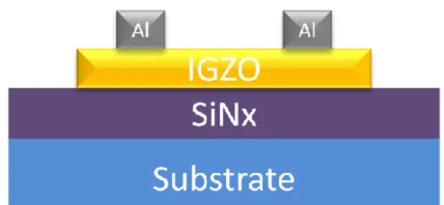
Fig. 1.3 The top-contact and bottom-gate a-IGZO TFT structure...9
Fig. 2.1 The a-IGZO TFTs fabrication process...19
Fig. 2.2 The passivation coating process...20
Fig. 3.1 Forward seven times sweeping of transfer characteristic of a-IGZO TFT...38
Fig. 3.2 Threshold voltage versus test sequence...38
Fig. 3.3 The (a) ID-VG curve (b) threshold voltage of the first and seventh measurement (c) measurement shift (d) mobility (e) sub-threshold swing of a-IGZO TFTs versus Oxygen ratio...39
Fig. 3.4 The sheet resistance versus O2 ratio...40
Fig. 3.5 The (a) ID-VG curve (b) threshold voltage and (c) threshold voltage shift (d) mobility and (e) sub-threshold swing of a-IGZO TFTs with various deposition temperatures...42
Fig. 3.6 The (a) ID-VG curve (b) threshold voltage (c) measurement shift (d) mobility (e) subthreshold swing of a-IGZO TFTs with various deposition power...44
IX
mobility and subthreshold swing of a-IGZO TFTs under various
process pressure...46
Fig. 3.8 The shifts of positive and negative bias stress at 5000sec. versus
Oxygen ratio...47
Fig. 3.9 The energy band diagrams under (a) positive bias stress and (b)
negative bias stress...48
Fig. 3.10 The (a) ID-VG curve (b) threshold voltage (c) mobility (d)subthreshold
swing of post-annealing a-IGZO TFTs deposited in various Oxygen
ratio...59
Fig. 3.11 The shifts of positive and negative bias stress at 5000sec. versus
post-annealing a-IGZO TFTs deposited in various Oxygen ratio...50
Fig. 3.12 The change of transfer curve from as-deposited phase to RTA
process(a) 6.67% (b) 50% (c) 80% of O2 ratio...51
Fig. 3.13 The (a) ID-VG curve (b) threshold voltage (c) mobility (d)subthreshold
swing of a-IGZO TFTs versus Oxygen ratio...52
Fig. 3.14 The shifts of positive and negative bias stress at 5000sec. versus
passivated a-IGZO TFTs deposited in various Oxygen ratio...53
Fig. 3.15 The transfer characteristics of a-IGZO TFTs deposited at 0.16% of
Oxygen ratio versus three treatment phases...54
X
(d) On/off ratio of a-IGZO TFTs in three treatment phases versus
various Oxygen ratios...55
Fig. 3.17 The stability evolution of three treatment phases versus various
deposition Oxygen ratios...56
Fig. 3.18 The transfer characteristic curves of 10000-second (a) positive and (b)
negative stability examination...57
Fig. 3.19 The threshold voltage shifts under (a) positive and (b) negative
stability examination with duration of 10000-sec, and fitting curve....58
Fig. 3.20 The extraction parameters of (a) positive, and (b) negative stability examination...60
XI
Table Captions
Table 3.1 The sheet resistance of as-deposited a-IGZO films versus various
power and pressure deposition...61
Table 3.2 The sheet resistance of post annealing a-IGZO films versus various
power and pressure deposition...61
Table 3.3 The extraction parameters of a-IGZO TFTs deposited at 0.16% of
1
Chapter 1
Introduction
1-1 An overview of metal oxide semiconductors TFTs
Thin-film transistors (TFTs) based on metal oxide semiconductors were considered as a promising candidate for next generation semiconductor. [1] Applications of liquid-crystal displays, electrophoretic displays, and especially organic light-emitting diode displays by using metal oxide TFTs (AMOLEDs) has attract much attention for it in recent years. Particularly, high performance of amorphous In-Ga-Zn oxide (a-IGZO) as active layer of TFTs exhibited a high mobility of >10 cm2/Vs-1 and a good sub-threshold swing (SS) of 0.2 V/decade in a-IGZO TFTs [2-3]. Moreover, the capability of low process temperature, high transparency, and uniformity are also importance features of a-IGZO TFTs. [4-5] In addition, big band gap (>3eV) of a-IGZO material result in insensitivity of natural light and transparent in visible region (λ=400nm~700nm). The carrier concentration of a-IGZO film was also controllable by modulating oxygen ratio, process power and pressure.
The radio-frequency sputtering is one of methods to deposit a-IGZO film, which enables to deposit thin films of high-melting-temperature materials over large areas at low substrate temperatures. [6] Nevertheless, H. Hosono et al. proposed that the chemical species and/or a structure in a thin film are unstable when thin films are
2
deposited at low temperatures. [6-7] Instead, they were stable while thin films were deposited at high temperatures. The chemical species and/or a structure are frozen in the as-deposited thin film which relax to a more stable state and give the atoms more energy to rearrange upon thermal annealing, leading to an appreciable change in the electron transport properties. [6-7] Most oxide TFTs especially a-IGZO TFTs, are fabricated using physical vapor deposition (PVD) techniques at room temperature and often require a high temperature (>300℃) post-deposition thermal annealing process to get high-performance and high-stability TFTs. [6-12]
1-2 Carrier transmission mechanism of metal oxide semiconductors
Compare to a-IGZO and the conventional material-hydrogenated amorphous silicon (a-Si:H) transmission mechanism, the a-Si:H material composed with covalent bonds of sp3 orbital was easily affected by the ordering of the structure. As shown in Fig. 1.1.[13] The electronic levels and trap states was influenced by the fluctuation of the bonding angle in the a-Si:H structure. [13] However, the amorphous oxide semiconductors (AOSs) are quite different. As shown in Fig. 1.2. The bottom of the conduction band in the oxide semiconductors that has large ionicity is primarily composed by spatially spread metal ns (here n is the principal quantum number) orbitals with isotropic shape. [13]Each element in this ternary material of a-IGZO film showed various characteristics to affect the parameters of TFTs. A high concentration of In atom is
3
expected to generated high carrier. [14] The element of In is a big atom and easy to lose electrons while the oxygen is a small atom and easy to get electrons from In. The released electron from the element of In may move to the conduction band when the composition of a-IGZO is lacked for oxygen. [15] It will enhance the carrier transport during the operation in TFTs. Ga was chosen because of atomic radius of Ga is closed to In. Hosono et al. reported that the Ga3+ in the a-IGZO film attract the oxygen tightly due to the high ionic potential resulted from the small ionic radius and +3 valence. It suppresses the electron injection and induces the oxygen ions escaping from the a-IGZO film, providing relative high stability to the device. [16] Compare to the carrier concentration in the material of IZO (~1021 cm-3), smaller carrier concentration of a-IGZO (~1019 cm-3) was observed. [16-18] However, Ga helps the carrier concentration of the a-IGZO film to be controlled easily. The element of Zn in the a-IGZO film was rported to affect the crystallization of the thin film. When the ratio of the Zn atoms in the a-IGZO film is larger than 65%, the crystalline structure was reported. [15] The crystalline structure in the a-IGZO film may degrade the electrical characteristic while the uniformity was decreased by the disorder grain boundaries.
4
1-3 Post treatment
Low temperature process metal oxide TFTs consist unstable characteristics of performance. Large energy must be given to rearrange atoms which developed at low temperature. Post treatment on a-IGZO film on substrates of Silicon wafer, glass, and flexible substrate had been investigated in recent years. For silicon wafer and glass substrates, one of methods to solve the unstable issue is post thermal annealing. As for post-deposition thermal annealing techniques, rapid thermal annealing (RTA) [10, 11] or furnace annealing (high vacuum or atmosphere) [12] are often used to anneal the oxide TFT devices. The activation energies of the Hall mobility in the as-deposited, low temperature, unoptimized films had larger values than annealed films were observed. [12] It indicated that the thermal annealing reduces the density of the shallow localized states beneath the conduction band minimum. [7] Moreover, an excellent correlation was found among the Hall mobility, field effect mobility, and the reduction in the absorption tail intensity for the low-temperature a-IGZO films with increasing temperature of post-annealing. [7] As a result, post-annealing had been a necessary process to stabilize and enhance performances of metal oxide devices.
The metal oxide TFT may degrade when the device is exposed to H2 and O2 atmosphere without a proper insulation. [19] Developing passivation layer to protect a-IGZO film from ambient atmosphere is a solution for this issue. In addition, the
5
a-IGZO TFTs characteristics also vary with the development conditions of passivation layer. Passivation species and development conditions must be carefully controlled. Organic passivation materials were chosen and used in this thesis, in order to reduce degradations of the performance of the device.
1-4 Motivation
Stability had been a big issue for metal oxide TFTs, especially for promising, high performance a-IGZO TFTs. Although the good performance of a-IGZO was observed, [20] the dominant mechanism of device instability is still uncertain. [20-22 ,2] As for amorphous Si (a-Si) TFTs, the instability mechanism of the device has been attributed to charge trapping in the gate dielectric or state creation in a-Si. The a-Si bonding structure is due to its sp3 orbital, [2] while the a-IGZO bonding structure is due to the large difference in electronegativity between the heavy metal cations and oxygen atoms.
Methods to solve unstable characteristics of a-IGZO film including deposition techniques of a-IGZO film, different structures of device, annealing techniques and passivation had been investigated in recent years. [13,24]As for deposition techniques, RF sputtering system is a common and promising instrument, [20] and was used in this thesis. RF sputter can fabricate a-IGZO films at room temperature but unstable and unoptimized characteristics were observed. In the process of RF sputtering, a relative stable a-IGZO film was observed with increasing temperature.
6
However, the a-IGZO film was still under an unstable condition. The characteristics of a-IGZO films also vary with the pressure, thickness, power in deposition process. To optimize the as-deposited a-IGZO to a stable and a high-performance condition by low-temperature sputtering is very inclinational.
Thermal annealing techniques are used to lead the metal oxide films to a more stable state and give the atoms more energy to rearrange. [6,7] An effective temperature range for anneal the a-IGZO film T >300℃ was observed, [24] which improve the electron transport properties of the as-deposited films fabricated at the unoptimized condition. However, a-IGZO film was very sensitive to the manufacturing processes. Thus, the top-contact and bottom-gate a-IGZO TFT structure, as showed in Fig. 1.4 has an advantage to protect the active channel, because the a-IGZO film was deposit in the end process. [19,23] Nevertheless, the performance of this type of structure may affected by ambient atmosphere. The instability of a-IGZO TFTs may be attributed to the interaction between the exposed backchannel and oxygen or water in the ambient atmosphere. [2] Development of a proper passivation to protect the a-IGZO film may leading to a more stable and reliable condition. [19] The spices and development process of passivation must be carefully executed without varying the characteristics of the device.
7
1-5 Thesis outline
In chapter 1, we introduced the advantage and potential of a-IGZO based transistor. Then carrier transmission mechanism was also introduced. The needs of post-treatment (annealing and passivaition) are shown. The experiment setup, instrument and extraction parameters will be introduced in chapter2. The stability under different deposition conditions and post-treatment are shown in chapter3. In chapter4, we make a conclusion of our experiments and future work.
8
Figures of Chapter 1
Fig. 1.1 The carrier transport paths in covalent semiconductors [13].
9
10
Chapter 2
Experiment Setup
2-1 Experimental procedure
In this section, device structure and process flow of the a-IGZO based TFTs using SiNx as dielectric were illustrated.
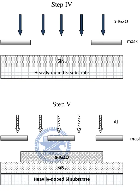
2-1.1Sample preparation(wafer)
As shown in Fig. 2.1, a 6-inch p-type heavily-doped silicon wafer is used as substrate and gate electrode for fabricating top-contact bottom-gate TFTs.
1.
Deposition of SiNx dielectric
1000 silicon nitride (SiNx) developed dielectric layer to fabricate a-IGZO TFT devices. The SiNx layer was deposited using low pressure chemical vapor
deposition(LPCVD) at 780℃ with gases: NH3 and SiH2Cl2 induced.
2.
Remove SiNx on backside
The backside silicon nitride on the silicon wafer, was etched by reactive ion etching (RIE). Prior to etching SiNx , photo resist FH-6400 was coated on the foreside of silicon wafer for protection. To remove SiNx layer on the back electrode of subtract, gases including Oxygen(O2) 5sccm and Tetrafluoromethane (CF4) 80sccm were induced. The process pressure and RF power were controlled about 15.0 Pa and 100W respectively. After the RIE process, photo resist FH-6400 on the
11
foreside of silicon wafer was removed by using Acetone. After, the SiNx/wafer clean process including SC1 and SC2 was required.
3.
Deposition of a-IGZO layer
The a-IGZO layer was deposited in Ar/O2 mixture at different temperature by RF magnetron sputtering, and patterned by shadow mask in Fig. 2.1. The 3-inch IGZO4 target with a molar ratio (In:Ga:Zn:O) of 1:1:1:4 was used. In sputter process, the pre-sputter was executed at powers of 30W and 70W at 5x10⁻² torr for 200 seconds in each power. In deposition process, powers at 50W, 70W and 100W were used. The temperature range from room temperature to 200℃and the deposition pressure range from 3mtorr to 9mtorr were used. Modulation of thickness range from 25nm to 90nm and O2 ratio (O2/Ar+O2) range from 0% to 0.3125% were used for fabricate different characteristics of IGZO layer. After deposition, power at 50W for200 seconds was proceeded for cooling the target temperature.
4.
Annealing
In this thesis, atmospheric anneal furnace was used to anneal. The annealing temperature is range from 350℃ to 400℃ with a flow ratio 10L/min. of Nitrogen (N2) in the furnace. The annealing time started after the furnace temperature was
stabilized was about one hour.
5.
Deposition of the Source/Drain electrode
12
Al were used as the source/drain electrodes on the a-IGZO TFTs. A 100nm thick Ti film was deposited using electron beam evaporator and a 100nm thick Al film was deposited by using thermal coater. Both (Ti and Al) electrodes were patterned by shadow mask as the source and drain electrodes of top-contact bottom-gate TFTs. The channel length and width of the fabricated a-IGZO TFTs were 400μm and 1000μm, respectively.
6.
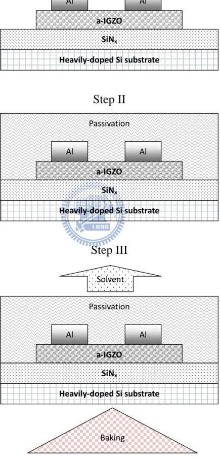
Passivation
Two kinds of organic materials were used as passivation layer of a-IGZO TFTs devices: PVP and PC-551. The spin coater was used to fabricate the passivation layer, with initial spin speed 800rpm for 10s and final spin speed 1200rpm for 24s as
shown in Fig. 2.2. After solutions were spin-coated on the device, baking process was proceeded at temperature 200℃ for 1 hour.
2-2 Operation mechanism and parameter of transistor
2-2.1
Operation mechanism
The a-IGZO TFT is an n-channel material and positive voltage is needed to form a channel. The channel is where delocalized electrons accumulate near the active layer/insulator interface when a positive voltage was applied to the gate electrode. As the channel was formed, a positive voltage applied to the drain electrode of the TFTs, these delocalized electrons in the accumulation layer are extracted from the channel, giving rise to drain current path through the TFTs. The
13
laser section we will report the definition of linear region and saturation region and their current function.
2-2.2
Linear region
As a small positive drain voltages, i.e., voltages smaller than the gate voltage minus the threshold voltage, VDS<VGS-VTH, the drain current conduction can be modeled as a linear relationship as is given by
μ O G TH (2-1) where the threshold voltage(VTH) is the voltage at which the intercept point of the square-root of drain current versus voltage when the device operate in saturation mode, COX is the oxide capacitance, μ is the mobility of the electrons, W is the width of the channel, L is the length of the channel. VGS and VDS are the gate-to-source and drain-to-source voltage, respectively.
2-2.3
Saturation region
As the drain voltage reaches the pinch-off voltage, i.e., the voltage at the channel near the drain is depleted of carriers, thus the current independent of the drain voltage and is given by
μ (2-2)
2-2.4
Mobility
Mobility is a parameter of how fast carriers can move in material. A higher magnitude of mobility allows for a faster switching time, i.e., the time it takes for the
14
device switching from the off state to on state. A large moblility value means that the device can conduct more current. Generally, mobility can be extracted from the transconductance maximum gm in linear region:
μ (2-3) The saturation mobility is another commonly used type of mobility. It is extracted from an ID-VG curve when the device is biased in saturation. [25]
2-2.5
Threshold Voltage
Threshold voltage is related to the operation voltage and power consumptions of TFTs. We extract the threshold voltage from equation (2-5), the intercept point of the square-root of drain current versus voltage when the devices operate in saturation mode.
μ (2-5)
2-2.6
I
ON/I
OFFcurrent ratio
The I ION/IOFF (on/off) ratio represents large turn-on current and small off current. It is an indicator of how well a device will work as a switch. A large on/off current ratio means there are enough turn-on current to drive the pixel and low off current to maintain in low consumption. In this thesis, the on current of the device was defined the drain current at VG=20V.
2-2.7
Sub-threshold swing
15
state to on state, which also represents the interface quality and the defect density..
(2-6)
2-2.8
Stress method and fitting model
The stress duration of the device was set for 5000 seconds and 10000 seconds. Measurements of the ID-VG curve within the stress procedure was set at 10s, 110s, 310s, 610s, 1010s, 1510s, 2010s, 3010s, 4010s, 5010s, 6010s, 7010s, 8010s, 9010s, 10010s. Two different voltage bias stresses were set: VG=20V and VG=-20V for positive stress and negative stress, respectively.
The fitting model was the stretched-exponential equations for the time dependence of threshold voltage shift in the stress procedure were defined as
(2-7) where at the infinite time, represent the characteristic time constant, is stretched-exponential exponent.[26]
2-3 Experimental instruments
2-3.1. Radio Frequency Magnetron Sputtering
Several methods are reported to deposit a film on to a substrate. Chemical vapor deposition (CVD) and physical vapor deposition (PVD) are the most commonly used to form and deposit a film in semiconductor-based area. Sputter is one of the
16
deposition techniques in PVD and it can be divided into two kinds of sputtering methods: Radio frequency (RF) sputtering and direct current (DC) sputtering. RF sputtering in wildly used to deposit a-IGZO in recent years. It uses a radio frequency of 13.56 MHz to generate plasma. The generated plasma creates ions to sputter the target material. The ions are accelerated towards the target by a negative DC bias on the target due to the flux of electrons. Generally, the RF sputtering is performed at the pressure of 1-50mtorr to improve the quality and the deposition rate of the deposited film. The quality of the thin film deposited at the low pressure was
increased due to the increased mean free path. Large mean free path help the species to find a stable state and to form a high quality thin film.
2-3.2. Electron beam evaporation
Electron beam evaporation (E-beam) is used to deposit titanium (Ti) contact layer in this thesis. Electrons emitted from hot filament by heating the filament and
accelerated into the metal source. Typically, 1 Ampere can generate energy of 10 kW which can evaporate many metals. The filament is isolated to avoid for contaminated by evaporant. The pressure of deposition process is under 5×10⁻⁶ torr or less.
2-3.3. Thermal evaporation
Material aluminium (Al) was deposited as the contact layer by using thermal evaporation. The thermal evaporation deposition technique consists of heating the metal to evaporate and deposit on the cold substrate. The process pressure was
17
controlled about 5×10⁻⁶ torr to avoid the vapor to react with atmosphere. The average energy of the vapor atoms reaching to the substrate surface is about 10 eV.
2-3.4. Spin coater
Spin coating process is suitable especially for dissolvent materials. The
passivation layer can be fabricated by spin coating. The initial spin speed determined the thickness of thin film, and the final spin speed determined the uniformity of the film. After spinning, the baking process is proceeded to evaporate the solvent of the solution to form the passivation layer.
2-3.5. Four-point probe resistivity measurement
The four-pint probe configuration is usually used to measure the sheet resistance of a semiconductor. Four identical probes are placed are placed in a linear
configuration, equally spaced, along the sample. Current is forced through the outer probes, while the voltage is measured across the inner probes. The voltage is
measured using a high impedance meter, which minimizes the current flow, thereby minimizing the contact resistance to a negligible value.
18
Figure of chapter 2
Step I
Step II
Step III
Heavily-doped Si substrate SiNx SiNx SiNx Heavily-doped Si substrate Heavily-doped Si substrate SiNx SiNx Etching Photoresist19
Step IV
Step V
Step VI
Fig. 2.1 The a-IGZO TFTs fabrication process. a-IGZO Heavily-doped Si substrate SiNx Al Al a-IGZO Heavily-doped Si substrate SiNx Heavily-doped Si substrate SiNx a-IGZO Al mask mask
20
Step I
Step II
Step III
Fig. 2.2 The passivation coating process. Passivation a-IGZO Heavily-doped Si substrate SiNx Al Al Solvent Baking Passivation a-IGZO Heavily-doped Si substrate SiNx Al Al a-IGZO Heavily-doped Si substrate SiNx Al Al
21
Chapter 3.
RESULT AND DISCUSSION
3-1 The rule of experiment parameters to determine the
insulator-to-conductor phases on as-deposited a-IGZO thin film.
Metal oxide is a flexible material with easily tunable phases that comprise insulator, semiconductor and insulator. Oxygen vacancy is an accepted electron donor in metal oxide material. Therefore, the oxygen quantity significantly influences the conductivity or carrier concentration in metal oxide. As regard to the application on semi-conductive metal oxide, the oxygen ratio controlling seems critical and important. Among metal oxide materials, amorphous In-Ga-Zn-O is one with easily controlled carrier concentration and acceptable mobility. RF sputter is an easily low-temperature deposition technique employed to grow metal oxide thin film likes a-IGZO. There are some experiment parameters that must be appropriately selected during thin film deposition process like working pressure, substrate temperature, gaseous component and RF power during thin film deposition. A set of experiment parameters could determine the final oxygen ratio or carrier concentration in a-IGZO film. In this study, we investigate the correlations between carrier concentration and the experiment parameters in detail. The study is expected to provide a useful guideline for a-IGZO deposition to attain a desired phases among22
insulator-to-conductor.
3-1.1
Oxygen ratio dependent characteristic during deposition
The thin film deposition process by RF sputtering proceeds with suppering gas to provide bombardment ions. Argon is the generally employed sputtering gas. In this study, oxygen is mixed with argon during thin film deposition. Oxygen is often used for oxide material deposition that could strongly influence the thin film property. In this study, the ratio of oxygen to mixture (oxygen ratio) is found to be a significant variable to directly determine the final oxygen quantity or carrier concentration in a-IGZO film. To study the oxygen ratio dependent conductivity (carrier concentration), the samples with various oxygen ratios are compared together while the working pressure and RF power are fixed as 3 mtorr and 100W, respectively.Fig 3.4 shows the sheet resistivity (Ω/㎝2
) as a function of oxygen ratio ranging from 0% to 0.34%. The samples are RF suptted a-IGZO films on glass substrate. Although a little variation on oxygen ratio (0%-0.34%), more than 5-order conductivity difference is attained. The material phase of a-IGZO film is transferred from conductor (104Ω/cm2) to insulator (109Ω/㎝2) with varying oxygen ratio during sputtering.
To verify the feasibility of a-IGZO films deposited with various oxygen ratios on the active layer in the a-IGZO thin film transistor. The transfer characteristics of
23
bottom-gate top-contact a-IGZO TFTs are presented in Fig. 3.3(a). The gate-controllable a-IGZO TFTs with oxygen ratio ranges from 0.1% to 0.23%. The IGZO active layer with oxygen ratio lower than 0.1% is too conductive to be completely depleted by negative gate to source bias. On the contrary, the IGZO active layer with oxygen ratio higher than 2.3% is too insulative to accumulate adequate mobile electrons under positive gate-to-source bias condition.
Besides, the as-fabricated a-IGZO TFTs without post-annealing meet a serious problem of moveable threshold voltage during device operation. To realize the instable behavior, 7-times sequent transfer curve measurements were made, as showed in Fig 3.1. All transfer characteristics are probed with fixed VDS of 20V and
sweeping VGS ranging from -15V to 20V. The threshold voltage shift (△Vth) defined
by the threshold voltage of seventh transfer curve minus the one of first transfer curve is used to simply judge the instability of a-IGZO TFT. Fig.3.3(b) shows the △Vth as a function of oxygen ratio. The magnitude and polarity of △Vth is strongly
dependent on the oxygen ratio in IGZO film. The detailed investigation of instability will be discussed in depth in section 3-2.
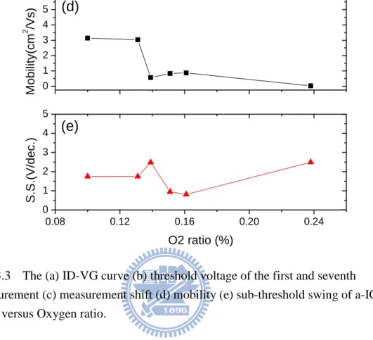
Mobility and sub-threshold swing are shown in Fig. 3.3(d), and Fig. 3.3(e), respectively. The mobility decreased dramatically with increasing O2 ratio. The sub-threshold swing degradations were found in the region oxygen ratio lower than 0.15% and higher than 0.16% The relative good oxygen ratio in the deposition
24
condition (100W, 3mtorr at room temperature) was in the region between 0.15% and 0.16% which exhibited relative good sub-threshold swing ~1 V/dec.
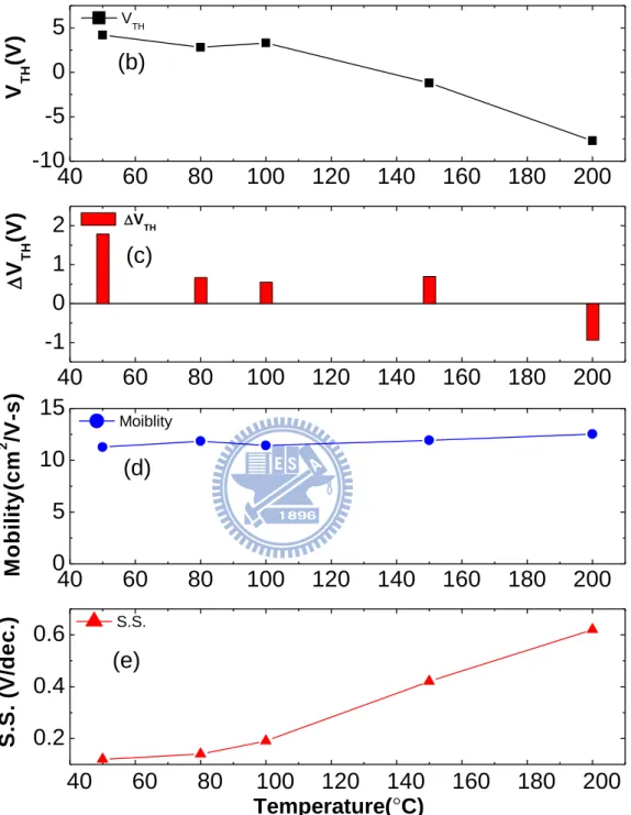
3-1.2
Temperature dependent characteristic during deposition
The transfer characteristics of a-IGZO TFTs with various substrate temperatures during IGZO active layer deposition are shown in Fig. 3.5(a). The samples with various substrate temperatures of 50°C, 80°C, 100°C, 150°C and 200°C are compared together. The RF power, working pressure and oxygen ratio of all samples during IGZO film deposition are 100W, 5mtorr and 0%, respectively. The thickness of a-IGZO layer in all samples is 35nm. The transfer curve (ID-VG curve) shift tonegative gate bias direction with increasing substrate. The negative shifted transfer curve indicates the over-high carrier current concentration that also destroys the controllability of gate and makes serious leakage current in body. The extracted threshold voltages from the firstly probed transfer characteristics of the a-IGZO TFTs with various substrate temperatures are presented in Fig. 3.5(b). △Vth calculated by
the first-time and the seventh-time transfer curves are also shown in Fig. 3.5(c). The result coincide the phenomena observed in section 3-1.1 that discuss the influence of oxygen ratio. The substrate heating is considered an action to reducing oxygen ratio in IGZO film. Here, the instability is also oxygen dependent. Higher oxygen ratio corresponds to more positive △Vth and lower oxygen ratio corresponds to more
25
negative △Vth. As compare to the device without substrate heating, the a-IGZO
TFT with higher temperature deposited active layer perform more stable although it is inadequate.
3-1.3
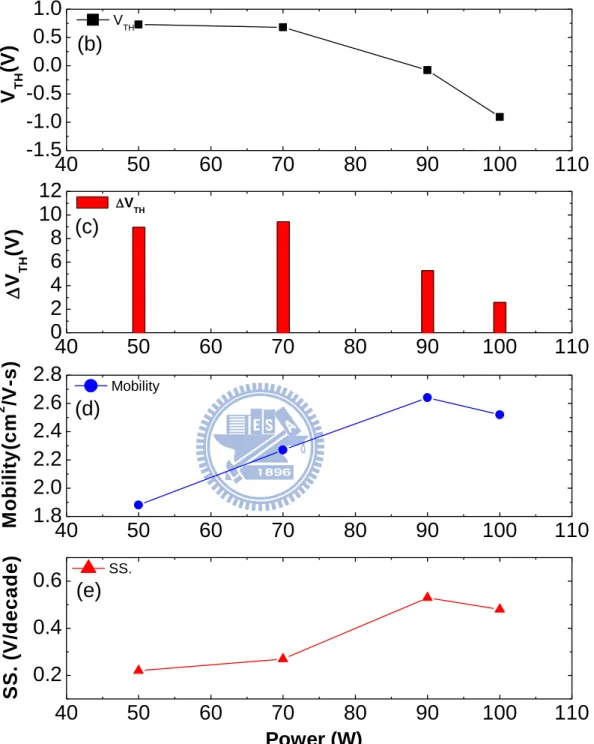
RF-Power dependent characteristic during deposition
Except the ration of oxygen to mixture gas and the substrate temperature, RF power and working pressure in chamber are also effective to the conductivity of a-IGZO film.
RF-power is also an important parameter during thin film deposition process. The resistivity or carrier concentration in a-IGZO film can be effectively controlled by RF power. [11] Fig. 3.6 shows the electric characteristics of a-IGZO TFTs with various RF-powers during active layer deposition while other parameters are fixed (pressure: 5mtorr, O2 ratio: 0%, Substrate temperature: room temperature). The threshold voltage of ID-VG curves is dependent on RF power and higher power
corresponds to more negative threshold voltage. As shown in Fig. 3.6 (a), a dramatic variation observed with RF power in a range between 70W and 90W. On the contrary, the transfer cure is insensitive to RF power lower than 70W. The transfer curve with lower threshold voltage always accompanied with more degraded sub-threshold swing resulted from leakage current in the body of active layer as shown in Fig. 3.6(e).
26
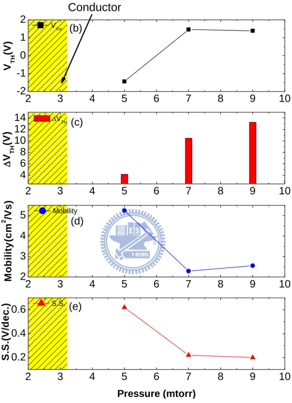
deposition
Fig. 3.7 shows the electric characteristics and extraction parameters of a-IGZO TFTs under various working pressures. Other deposition parameters are fixed at 100W of power, 0% of O2 ratio at room temperature. From Fig. 3.7(a), a conductor film was found at 3mtorr of pressure. TFT characteristics were found at 5mtorr, 7mtorr and 9mtorr, while the threshold voltage at 5mtorr is smaller compare with 7mtorr and 9mtorr. A trend was found in Fig. 3.7(c) with increasing of pressure, the positive threshold voltage shift increase. The mobility increases and sub-threshold swing degrades with decreasing of pressure, as shown in Fig. 3.7(d) and Fig. 3.7(e). Similar result can be found with increasing of power. The a-IGZO film tends to be conductive with lower working pressure, and a conductor film was found at 3mtorr. Nevertheless, films (5mtorr, 7mtorr, 9mtorr) were still in O2-rich phase because of positive threshold voltage shift was observed in the first measurement to the seventh measurement.
3-1.5
Adequately Controlled insulator-to-conductor phases by RF
power and pressure during deposition
From the last two sections, we found the electric characteristics from insulator to conductor phases of a-IGZO film are indeed controllable by modulating power and pressure in deposition process without introducing the oxygen gas. The sheet resistances of a-IGZO films measured by four-point probe resistivity measurement
27
under various pressure and power are shown in Table 3.1. Other process parameters are fixed at 0% of O2 ratio, 35nm of thickness at room temperature. The conductor film found in Fig. 3.7 (a) (3mtorr, 100W) exhibited the sheet resistance of ~1×10⁴
/cm2, which is smaller than other TFT characteristic films. As mentioned in section 3-1.1, the a-IGZO TFT with electric characteristics of TFT exhibited the sheet resistance range from ~1×10⁵ to ~1×10⁹ /cm2. The deposition condition exhibited the largest sheet resistance (>1010) and insulator film was located at 50W of power and 9mtorr of pressure (low power and high pressure), which is in the opposite trend of deposition condition as the conductor film did (high power and low pressure). To optimize the electric characteristic and conductivity of the a-IGZO TFTs, the Table 3.1 is a reliable reference data to be considered.
In the TFT-characteristic region (~1×10⁵ to ~1×10⁹ /cm2), the O2-lacked film and O2-rich film were found. While in the modulation of power and pressure, no near-conductor film was found. The sheet resistance table also shows that films are located out of the near-conductor region, from ~1×10⁵ to ~1×10⁶ /cm2. The phase changes of power and pressure modulation are significant and feasible. However the mobility of such a-IGZO devices, range from 2 cm2/V-s to 5 cm2/V-s, are higher than the device of O2 ratio modulation, range from 0.1 cm2/V-s to 3 cm2/V-s. The Oxygen induced in the RF-sputter deposition process may alter the formation of a-IGZO film.
3-2
Stability examination of as-fabricated a-IGZO TFT with
28
various oxygen Ratios (PhaseⅠ)
The stability examination of a-IGZO devices were implement by constant voltage bias stress. Two phases of stresses were used to examine the stability of the a-IGZO device: positive bias stress (VGS - VT0 = 20V, VDS= 0V) and negative bias
stress (VGS - VT0 = 20V, VDS= 0V) for 5000 seconds, where VT0 is the threshold
voltage before stress. The threshold voltage shifts under positive and negative bias stress for 5000 sec. in each deposition condition were listed as a group for comparison. Deposition conditions of various O2 ratios from near-conductor phase to near insulator phase were used as examination samples.
As shown in Fig. 3.3(b), the as-deposited a-IGZO films were very sensitive to the measurement sweep (VG=-15V~20V). The threshold voltage shift caused by
measurement was observed. To avoid the influence of measurement sweep of some samples, two devices were used for stress examination. One of two devices was measured first for extraction of threshold voltage (VT0). The other device was
stressed (VG-VT0=20V or -20V) for 5000-sec. without any measurement before. After
the stress duration was over, measurement was started to execute. The difference of threshold voltage between two samples was estimated as the threshold voltage shift caused by positive or negative bias stress.
3-2.1
Transfer characteristics
29
Phase change from conductor (0.08% of O2 ratio) to insulator (0.31% of O2 ratio) was observed, as mentioned in section 3-1.1. Samples between 0.1% to 0.23% of O2 ratio were chosen because of obvious electric characteristics performance of TFT.
3-2.2
Positive and negative gate-to-source bias stresses
The result of positive and negative gate-to-source bias stress shifts for 5000sec. versus various O2 ratios were shown in Fig.3.8. Both O2-rich and O2-lacked devices exhibited poor stability performance. The VT shift window defined by the distance between the VT shifts after negative and positive stress was always large. However, as for O2-rich devices (O2 ratio ≧0.14%), the negative stress performance were better than positive stress performance. An excellent stability of negative stress was found at 0.23% of O2 ratio, while it exhibited a poor stability in positive stress. On the other hand, good stabilities of positive stress were found at O2-lacked devices (O2 ratio of 0.1% and 0.13%), accompanied with poor negative stabilities. The result showed two phases devices (O2-lacked and O2-rich) exhibited either a good positive stability or a good negative stability. However, the device exhibited good stability in both directions (positive and negative) was not found. The VT shift window was still large in each device. The mechanism of the result is discussed in the next section.
The instability of theses devices were also found in measurement of VG
sweeping, as discussed in section 3-1. The measurement shift shown in Fig. 3.3(c), used for defining O2-rich ( ) and O2-lacked ( ) device, has
30
the correlation with the stress shift . The O2-rich device which exhibited a positive during measurement, showed a poor stability in positive stress, but a relative good stability in negative stress. In other hand, The O2-lacked device exhibited a negative , showed a good positive stability, but a poor negative stability. From this result we can verify: the threshold voltage shift during very short-term VG sweep ( ) can represent the instability of the long-term bias stress
instability of as-deposited a-IGZO TFT in either positive or negative stress direction.
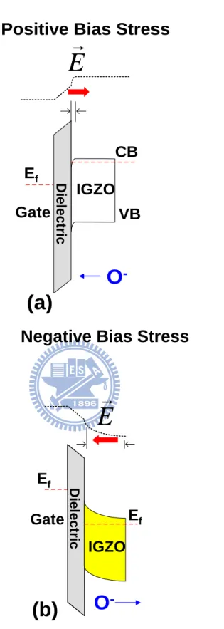
3-3 Proposed mechanism for instability of a-IGZO TFT.
Fig. 3.9 are the schematic diagrams to explain the oxygen related instability. Metal-oxide is considered the combination of oxygen ions and metal ions. Oxygen ions may be moved from the origin position by electric field. In Fig. 3.9(a), as the IGZO TFT is subjected to positive stress, the electric field in active layer almost exists near interface in accumulation condition. Higher oxygen concentration cause more collected oxygen ions with negative charge on the interface that result in positive threshold voltage shift. In Fig. 3(b), as the IGZO TFT is subjected to negative stress, the electric field exists in the body of active layer in depletion condition. Lower oxygen concentration indicates higher dopant concentration that result in higher electric field in depletion region. Higher electric field in the body results in more oxygen ions collect in the body that move the threshold voltage to negative direction.
31
3-4 Stability examination of thermally-annealed a-IGZO TFT with
various oxygen ratios (PhaseⅡ)
After examining stabilities of as-deposited a-IGZO TFTs, the thermal annealing process was executed to verity the functionality of the post thermal treatment. The Al contact electrodes are deposited after post-annealing to avoid the melting or diffusion of Al during high temperature annealing process. The post thermal annealing is performed by furnace and nitrogen gas is introduced during the process. The probed threshold voltage shifts of annealed devices during sequent transfer curve measurement are around 0.2V which seems significantly improved as compared with the as-fabricated devices.
3-4.1
Transfer characteristics
The transfer and electric characteristics of annealed a-IGZO TFTs with various oxygen ratios are shown in Fig. 3.10. The transfer curves seems consistent with each other as shown in Fig. 3.10(a). The divergent curves showed in Fig. 3.3(a) were unified and significantly improved by post annealing. The consistency was also found in threshold voltage (~4V) in Fig 3.10(b), mobility (~10 cm2/V-s) in Fig 3.10(c), subthreshold swing (~0.2 V/dec.) in Fig 3.10(d).
3-4.2
Positive and negative gate-to-source bias stresses
To follow the stability examination implanted on as-fabricated devices, the same bias stress conditions involves both positive and negative bias stress are also
32
executed on annealed a-IGZO TFTs. Fig 3.11 shows threshold voltage shifts under positive stress and negative stress with the duration of 5000-sec.. The a-IGZO TFT with the characteristic of conductor (O2 ratio of 0%, 0.08%) and insulator (O2 ratio of 0.31% ) in the first phase of as-deposited condition are also annealed and then examined. As showed in Fig 3.11, the annealed devices with various oxygen ratios during deposition process exhibits a smaller VT shift window, a well positive stability and an excellent negative stability. The VT shift under positive bias stress is ranged from 5V to 9V, and the one under negative bias stress is ranged from -0.2V to -0.8V. Each device exhibits consistent stabilities in both positive and negative direction.
3-4.3
Functionality of thermal annealing
The change of electric characteristics from as-deposited to annealed a-IGZO TFT is obvious. A significant improvement on sub-threshold swing, mobility, on/off ratio and stability is observed. The a-IGZO TFTs with active layers ranges from conductor to insulator in as-fabricated phases could be unified to an excellent condition by post-annealing. The annealing-improved device exhibits a well stability and the active layer is close to the O2-rich condition (stability is better in negative bias stress direction). According to the result, the functionality of post-thermal annealing are synthesized and speculated: To homogenizes the oxygen concentration in IGZO film and strength the bonding between atoms. The function of unifying by post-annealing can also be demonstrated by sheet resistance measurements as shown
33
in table 3.2. The of annealed a-IGZO films is deposited with various RF power and working pressure. The sheet resistances of these films arte unified to the value of 109Ω /cm2 which is belonged to the O2-rich film.
The phase changes of a-IGZO device can also be observed in rapid temperature annealing (RTA) process. Fig.3.12 showed the phase changes from insulator to conductor phases by using the RTA. The devices deposited with 6.67%, 50%, and 80% of O2 ratio were treated by the RTA process, 400°C for 5 seconds. The semiconductor characteristic was found with the deposition condition 6.67% of O2 ratio in as-deposited phase. The insulators were found in as-deposited phase of 50% and 80%. After the RTA process, the 6.67% and 50% of O2 ratio in as-deposited phase turned into conductors. The TFT characteristic was found in 80% of O2 ratio, after the process. The result suggested that the RTA process was a treatment, to reduce the O2 ratio in the a-IGZO film. The a-IGZO film (6.67% of O2 ratio) with smaller O2 and executed TFT characteristic in as-deposited phase turned into a conductor after RTA process. On the other hand, the a-IGZO film with larger O2 and executed insulator characteristic return to semiconductor characteristic after the process. The oxygen can be induced in and reduced from a-IGZO film by using the RTA process. The characteristic of a-IGZO film in as-deposited phase can be changed and oxygen in a-IGZO film homogenized by implementing various thermal annealing processes and conditions.
34
3-5
Stability examination of passivated a-IGZO TFT with
various oxygen ratios(PhaseⅢ)
Passivation layer was performed on the post-annealed a-IGZO TFT. The choice of passivation material is critical since the a-IGZO film is very sensitive to the post treatment involves passivation layer deposition. The passivation process must keeps mild to maintain the original electric characteristics. A proper passivation should possess well protection functionality without influencing the electric characteristics of the device. In this study, organic photoresistor (PR) was chosen to passivated the device. The passivation layer is formed by spin coating and then baking at 200°C for 1hr on the hotplate. The thickness of the PR layer was about 1m.
3-5.1
Transfer characteristics
Three as-fabricated a-IGZO TFTs with oxygen ratios including 0.1% (O2-lacked), 0.16% (middle), and 0.24% (O2-rich) were annealed and passivated. The transfer characteristics and the extracted parameters of the passivated a-IGZO devices were showed in the Fig 3.13. The transfer characteristics showed in Fig 3.13(a) demonstrated a consistent curve among the a-IGZO TFTs with various oxygen ratios during deposition process. The extracted parameters also show the consistency between each device, as showed in Figs 3.13(b), (c), (d). The values of threshold voltage, mobility, and sub-threshold swing are as 3 V, 12cm2/(V-s), and 0.14 V/dec., respectively. The comparison of as-deposited, annealed, and passivated
35
device are showed and discussed in section 3-6.
3-5.2
Positive and negative gate-to-source bias stresses
Fig 3.14 shows threshold voltage shifts under positive stress and negative stress with durations of 5000-sec.. The stability under positive bias stress of each device is enhanced significantly as compared with the un-passivated devices, while the stability under negative bias stress is maintained well. The average of threshold voltage shifts under positive bias stress and negative bias stress are around 2.5V and -0.6V, respectively. Here, the stability of the a-IGZO TFT is presented to reach an excellent condition under both polar bias stresses.
3-5.3 Functionality of passivation
An enhancement of stability under positive bias stress and no degradation on electric characteristics were found in passivated device. The passivation layer provided a protection layer to isolate the a-IGZO film from the oxygen-rich atmosphere. Oxygen is considered a source to induce a positively shifted threshold voltage under positive bias stress. [27]. In this study, an organic layer, photoresistor, forms a feasible protection layer without making reaction with the a-IGZO film.
3-6
Proposed procedure to attain entirely stable device
According to the results mentioned above, we demonstrated that the performance of the as-deposited a-IGZO TFT was tunable and sensitive to the process parameters like working pressure, substrate temperature, gaseous component
36
and RF-power. Nevertheless, the electric characteristics and stability of the device is far deviated from the optimized condition. The post-annealing process is thought to rearrange the atoms with a stronger bonding. The electric characteristics and stability under negative bias stress is improved significantly by post-annealing. Besides, the post-annealing in nitrogen atmosphere leads the film to an O2-rich condition. The positive stability was enhanced in depth by passivaion capping with photoresistor. The influence of ambient atmosphere was insulated by the passivation layer. Finally, the high-performance and high-stability a-IGZO TFT was obtained.
3-6.1
Synthetic comparison between three treatment phases
The transfer characteristics and extracted parameters of the a-IGZO TFT in various phases are compared together in Fig. 3.15 and Fig. 3.16, respectively. The evolution with various phases (as-deposited, annealed, and passivated) of transfer characteristic curves of a-IGZO TFT with 0.16% of oxygen ratio is clearly presented. In the as-deposited phase, the device exhibited a poor electric characteristic and unstable threshold voltage. In the anneal phase, a significantly improved and unified characteristic are observed. In the passivated phase, the excellent transfer characteristic is maintained although a little negatively-shifted threshold voltage.
The extracted parameters like threshold voltage, mobility, and sub-threshold swing of the a-IGZO TFTs with various oxygen ratios during deposition (0.1%, 0.16%, and 0.24% of O2 ratio) in three treatment phases are showed in Fig. 3.16.
37
The extracted parameters of the as-fabricated a-IGZO TFT with various oxygen ratios are unified to a significantly improved value by the post-annealing. The variation on electric characteristics of a-IGZO TFT is in-obvious during the phase transition from the second one (post-annealed) to the third one (passivated). The passivation layer is quite proper for the a-IGZO film that will not change the initial property. Fig. 3.17 shows the threshold voltage shifts under positive and negative bias stress with various oxygen ratios in three treatment phases.
3-6.2
Performance of final device
An a-IGZO TFT with high-performance and high-stability is fabricated by going through three treatment phases in order. The phases include as-fabrication, post-annealing and passivation. In this section, the stability under both polar bias stresses was examined during 10000-sec bias stress. The threshold voltage shift was fitted by the stretched-exponential equation model. A larger value of characteristic time constant ( ) and stretched-exponential exponent ( ) corresponds to a higher stability. The stability examination result is showed in Fig. 3.18, Fig. 3.19, and Fig. 3.20. The fitting parameters ( ) of positive stress and negative stress are 860000(0.3867) and 2138000(0.5614), respectively, which is comparable to the report data [28]. The extracted mobility and sub-threshold swing showed in Fig. 3.20 are stable during both positive and negative bias stresses. The emphasized advantage of the a-IGZO TFT in this study is the completely stable behavior under both
38
39
Figure in chapter 3
-5 0 5 10 15 20 10-13 10-12 10-11 10-10 10-9 10-8 10-7 10-6 10-5 10-4ID(A)
VG (V)
1st 2nd 3rd 4th 5th 6th 7thFig. 3.1 Forward seven times sweeping of transfer characteristic of a-IGZO TFT.
1 2 3 4 5 6 7 2 4 6 8 10 12 14 16 18 20
Thr
eshol
d vol
tag
e (V)
Test Sequence
Threshold voltage40 -12 -8 -4 0 4 8 12 V TH (V) VT 1st VT 7th
(b)
0.08 0.10 0.12 0.14 0.16 0.18 0.20 0.22 0.24 -6 -4 -2 0 2 4 6 8 O2 ratio(%) V TH (V)(c)
-15 -10 -5 0 5 10 15 20 10-13 10-12 10-11 10-10 10-9 10-8 10-7 10-6 10-5 10-4 10-3ID(A)
VG (V)
0.08% 0.1% 0.13% 0.14% 0.15% 0.16% 0.24% 0.31%(a)
0.31% 0.24% 0.16% 0.15% 0.14% 0.13% 0.1% 0.08%41 0 1 2 3 4 5 6 0.08 0.12 0.16 0.20 0.24 0 1 2 3 4 5 M obilit y (c m 2 /Vs )
(d)
S. S. (V/ dec .) O2 ratio (%)(e)
Fig. 3.3 The (a) ID-VG curve (b) threshold voltage of the first and seventh
measurement (c) measurement shift (d) mobility (e) sub-threshold swing of a-IGZO TFTs versus Oxygen ratio.
0.00 0.05 0.10 0.15 0.20 0.25 0.30 0.35 103 104 105 106 107 108 109 1010
S
hee
t Resistance
(
/c
m
2)
O2 ratio (%)
Conductor
Insultor
42
-15
-10
-5
0
5
10
15
20
10
-1410
-1310
-1210
-1110
-1010
-910
-810
-710
-610
-510
-410
-3 150
C 100
C 80
C 200
CID(A)
VG (V)
50C 80C 100C 150C 200C 50
C(a)
43
40
60
80
100
120
140
160
180
200
-10
-5
0
5
40
60
80
100
120
140
160
180
200
-1
0
1
2
40
60
80
100
120
140
160
180
200
0
5
10
15
40
60
80
100
120
140
160
180
200
0.2
0.4
0.6
(e)
(d)
(c)
V TH (V ) VTH(b)
V TH (V ) V TH M o b il it y (cm 2 /V -s ) Moiblity S .S . (V /d e c .) Temperature(°C) S.S.Fig. 3.5 The (a) ID-VG curve (b) threshold voltage and (c) threshold voltage shift (d) mobility and (e) sub-threshold swing of a-IGZO TFTs with various deposition temperatures.
44
-20
-15
-10
-5
0
5
10
15
20
25
10
-1410
-1310
-1210
-1110
-1010
-910
-810
-710
-610
-510
-410
-3ID(A)
VG (V)
50W 70W 90W 100W 50W 70W 90W 100W(a)
45
40
50
60
70
80
90
100
110
-1.5
-1.0
-0.5
0.0
0.5
1.0
40
50
60
70
80
90
100
110
0
2
4
6
8
10
12
40
50
60
70
80
90
100
110
1.8
2.0
2.2
2.4
2.6
2.8
40
50
60
70
80
90
100
110
0.2
0.4
0.6
(e)
(d)
(c)
V TH (V ) V TH(b)
V TH (V ) V TH M o b il it y (cm 2 /V -s ) Mobility S S . (V /d e c a d e ) Power (W) SS.Fig. 3.6 The (a) ID-VG curve (b) threshold voltage (c) measurement shift (d) mobility (e) sub-threshold swing of a-IGZO TFTs with various deposition power.
46
-5
0
5
10
15
20
10
-1310
-1210
-1110
-1010
-910
-810
-710
-610
-510
-410
-310
-2 3mtorr 7mtorrID(A)
VG (V)
3mtorr 5mtorr 7mtorr 9mtorrConductor
9mtorr 5mtorr(a)
47
2
3
4
5
6
7
8
9
10
-2
-1
0
1
2
2
3
4
5
6
7
8
9
10
4
6
8
10
12
14
2
3
4
5
6
7
8
9
10
2
3
4
5
2
3
4
5
6
7
8
9
10
0.2
0.4
0.6
V TH (V ) V THConductor
(b)
(e)
(d)
(c)
V TH (V ) V TH M o b il it y (cm 2 /V s ) Mobility S .S .( V /d e c .) Pressure (mtorr) S.S.Fig. 3.7 The (a) ID-VG curve (b) threshold voltage and measurement shift (c) mobility and subthreshold swing of a-IGZO TFTs under various process pressure.
48
0.00
0.05
0.10
0.15
0.20
0.25
0.30
0.35
-25
-20
-15
-10
-5
0
5
10
15
20
25
V
TH(V)
O
2ratio (%)
Negative Stress Positive StressFig.3.8 The shifts of positive and negative bias stress at 5000sec. versus Oxygen ratio.
![Fig. 1.1 The carrier transport paths in covalent semiconductors [13].](https://thumb-ap.123doks.com/thumbv2/9libinfo/8756098.206938/21.892.244.714.177.833/fig-carrier-transport-paths-covalent-semiconductors.webp)

![TraditionalMLCalgorithmsmainlytacklethebatchMLCproblem,wheretheinputdataarepresentedinabatch[24,28].Nevertheless,inmanyMLCapplicationssuchase-mailcategorization[22],multi-labelexamplesarriveasastream.Onlineanalysisistherefore dimensionreducermotivatedbyma](data:image/gif;base64,R0lGODlhAQABAIAAAP///wAAACH5BAEAAAAALAAAAAABAAEAAAICRAEAOw==)