國
立
交
通
大
學
電子工程學系 電子研究所碩士班
碩
士
論
文
四埠射頻金氧半電晶體與共用源汲極主動區之
新型串疊結構的小訊號等效電路模型
建立與驗證
Small Signal Equivalent Circuit Models Development
and Verification for Four-port RF MOSFET and New
Cascode Structure with Merged Source Drain Diffusion
研 究 生:邱德昌
指導教授:郭治群 博士
I
四埠射頻金氧半電晶體與共用源汲極主動區之新型串疊結構的小
訊號等效電路模型建立與驗證
Small Signal Equivalent Circuit Models Development and
Verification for Four-port RF MOSFET and New Cascode
Structure with Merged Source Drain Diffusion
研 究 生:邱德昌 Student:De-Chang Chiu
指導教授:郭治群 博士 Advisor:Dr. Jyh-Chyurn Guo
國 立 交 通 大 學
電子工程學系 電子研究所
碩 士 論 文
A Thesis
Submitted to Department of Electronics Engineering and Institute of Electronics College of Electrical and Computer Engineering
National Chiao Tung University in partial Fulfillment of the Requirements
for the Degree of Master of Science in
Electronics Engineering September 2011
Hsinchu, Taiwan, Republic of China
II
四埠射頻金氧半電晶體與共用源汲極主動區之新型串疊結
構的小訊號等效電路模型建立與驗證
學生:邱德昌 指導教授: 郭治群 博士
國立交通大學 電子工程學系 電子研究所碩士班
摘要
本論文中,建立了小訊號等效電路模型,其中包括新型基板網路模型及其參數萃取 方法,以應用於含有深 N 型槽(deep n-well)的射頻互補式金氧半場效電晶體電路模擬 上。本研究設計四端點的射頻金氧半電晶體於四埠測試結構,並利用 UMC 65 奈米互補 式金氧半場效電晶體製程(UN65)研製出來探討元件高頻特性及模型的發展。本論文提出 之新型基板網路模型,具備完整之參數萃取流程並且解決了傳統模型與 BSIM-4 內建模 型之問題。此基板網路模型乃是四埠元件小訊號等效電路模型之核心,直接影響四埠散 射參數模擬之準確性,並且能夠簡易地取代 BSIM-4 內建模型以改進其四埠元件模擬之 嚴重誤差。所建立的小訊號等效電路模型在不同偏壓進行模擬以作廣泛的驗證,其準確 性已證明可應用於高達 40GHz 的寬頻範圍,以及不同的偏壓條件如截止區、線性區與 飽和區。此外,本論文涵蓋 BSIM-4 模型之參數校正以及探討基板效應與電容模型中內 部電荷計算方法。 論文的第二部份為新型串疊結構之設計與小訊號等效電路模型研發,其構成元件為共 用源汲極主動區之雙閘極金氧半場效電晶體。此小訊號等效電路模型亦在不同偏壓下透 過模擬做廣泛的驗證。再者,為了能夠同時模擬雙閘極金氧半場效電晶體大訊號特性與 小訊號特性,我們利用 BSIM-4 建立傳統的串疊結構,即二個串疊之電晶體,並外掛寄III
生元件和調整 BSIM-4 參數以近似雙閘極金氧半場效電晶體模型,並透過模擬做廣泛的 驗證,以應用於 40GHz 的寬頻範圍。
IV
Small Signal Equivalent Circuit Models Development and
Verification for Four-port RF MOSFET and New Cascode
Structure with Merged Source Drain Diffusion
Student:De-Chang Chiu Advisor:Dr. Jyh-Chyurn Guo
Department of Electronics Engineering
Institute of Electronics
National Chiao Tung University
Abstract
In this thesis, small signal equivalent circuit models have been established for 4-port RF MOSFET and new cascade structure. For the first time, a new body network model is developed for RF MOSFET fabricated with UN65 process in which the 4-port test structure was arranged with p-well body and deep n-well tied together to one port for body terminal. The proposed body network model is supported with a comprehensive model parameters extraction method and can be easily integrated with intrinsic MOSFET to build a small signal equivalent circuit model. The simulation accuracy has been proven by good match with measured 4-port S-parameters up to 40GHz and under different operation conditions, such as off-state, linear region, and saturation. On the other hand, the simulation using BSIM-4 with default body network fails to predict 4-port S-parameters with particularly large deviation in the parameters related to body node. The problem with BSIM-4 can be solved by replacing the default model with our new body network model.
V
In the second part, a small signal equivalent circuit is developed for new cascode structure, which is a kind of dual gate MOSFET with merged source/drain diffusion region. A modified body network model is adopted to match different configurations in deep n-well and p-well body. 4-port S-parameters can facilitate the extraction of complicated model parameters in dual gate MOSFET, such as in-stage capacitances, inter-stage capacitances, and cross-stage capacitances. The small signal equivalent circuit model built with core model for dual gate MOSFET and modified body network model demonstrates acceptable simulation accuracy at off state and saturation region. BSIM-4 is utilized to approach new cascode structure by incorporating parasitic elements such as inter-stage resistance and capacitances into conventional cascode with two single MOSFETs and enable both small signal and large signal simulations.
VI
誌謝
首先,我要感謝我的指導教授--郭治群教授。過去三年多來在研究方法及態度上的指導, 不斷地替學生尋找研究資源,並且嚴格要求學生完成許多基礎工作。在這過程中,除了 建立許多研究領域相關的能力,也體會到許多待人接物的觀念,相信將會成為我未來工 作上或者研究上的準則。 此外,還要感謝 NDL 的研究員—鄧裕民,在研究設備上的支持,讓我能夠接觸並 學習到高頻量測設備。也感謝 RFTC 的工程師們,劉汶德在量測實驗上的協助以及建議, 讓我能夠順利完成量測。 感謝 LAB635 中的所有成員們,敬文學長、智友學長、弈岑學長、唯倫、智翔的 陪伴 ,讓我在實驗室的生活更豐富有趣。 最後,我要感謝一直在背後支持我的家人。VII
Content
Chinese Abstract ... II English Abstract ... IV Acknowledgement ... VI Content... VII Figure Caption ... IX Table Caption ...XXIChapter 1 Introduction ... 1
1.1 An Overview and Motivation ... 1
1.2 Thesis Organization ... 3
Chapter 2 Fundamental theory ... 5
2.1 Scattering Matrix and Parameters ... 5
2.1.1 Two–port network and scattering parameters... 5
2.1.2 Four –port scattering matrix and parameters ... 5
2.1.3 Port reduction method ... 6
2.2 RF Amplifier Design Consideration ... 6
2.2.1 Impedance matching ... 7
2.2.2 Power gain and voltage gain ... 7
2.2.3 Noise [1] ... 9
Noise Factor... 9
2.2.4 Linearity[3] ... 11
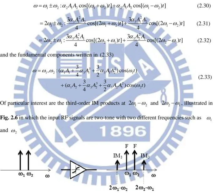
2.2.5 Intermodulation [3] ... 13
2.2.6 Stability [4] ... 16
Chapter 3 Four-port RF MOSFET Modeling for Simulation with DBB ( UN65 CMOS Technology) ... 18
3.1 Four-port RF MOSFET Layout and Measurement ... 18
3.1.1 4T MOSFET Layout Analysis for Body Network Model Development ... 19
3.1.2 4T MOSFET Layout Analysis for Parasitic RLC Extraction ... 25
3.1.3 4-port RF MOSFET Measurement and De-embedding Method ... 27
3.1.4 4-port RF MOSFET Parasitic RLC Extraction Results and Comparison with 2-port Structure ... 33
VIII
3.2.1 Review of Previous Work ... 39
3.2.2 Improved Body Network Model-Equivalent Circuit and Extraction Method... 43
3.3 Four-port RF MOSFET Small Signal Equivalent Circuit Development and Analysis ... 52
3.3.1 Small Signal Equivalent Circuit at Off State ... 52
3.3.2 Small Signal Equivalent Circuit in Linear Region ... 63
3.3.3 Small Signal Equivalent Circuit in Saturation Region ... 72
3.4 BSIM-4 with Improved Body Network Model for Four-port RF MOSFET Simulation ... 84
3.4.1 BSIM-4 I-V Model Calibration and Simulation for 65nm 4-port RF MOSFET with DBB - UN65 L65003 ... 85
3.4.2 BSIM-4 C-V Model Calibration and Simulation for 65nm 4-port RF MOSFET with DBB - (UN65 L65003) ... 100
3.4.3 . RF Performance of 4-port RF MOSFET with DBB – Simulation and Measurement ... 118
Chapter 4 New Cascode Design and Modeling for RF Circuits Simulation ... 121
4.1 Review of Conventional Cascode Structure for RF Amplifiers ... 121
4.2 New Cascode using Dual Gate MOSFET with Merged S/D Diffusion ... 124
4.2.1 Comparison between New Cascode and Conventional Cascode Structures... 127
4.2.2 Dual-gate MOSFET Measurement and Deembedding Method ... 128
4.3 Dual-gate MOSFET Equivalent Circuit Model and Parameters Extraction Method for New Cascode Simulation ... 133
4.3.1 Small Signal Equivalent Circuit Model of Dual-gate MOSFET at Off State ... 136
4.3.2 Small Signal Equivalent Circuit Model of Dual-gate MOSFET at Active State ... 153
4.4 Dual-gate MOSFET Simulation by BSIM-4 with Parasitic RLC Parameters ... 163
4.4.1 BSIM-4 I-V Simulation for Dual-gate MOSFET ... 163
4.4.2 BSIM-4 C-V Simulation for Dual-gate MOSFET ... 167
4.4.3 High Frequency S-parameters Simulation and Comparison with Measurement . 168 Chapter 5 Conclusions and Future Work ... 178
5.1 Conclusions ... 178
IX
Figure Caption
Fig. 2.1 Traditional transistor-amplifier of input matching... 7
Fig. 2.2 (a) MOSFET‘s power gain comparisons between simulation and measurement ... 9
Fig. 2.3. Noisy two-port driven by noisy source ... 10
Fig. 2.4. Equivalent circuit for two-port noise model ... 10
Fig. 2.5 Definition of the 1-dB compression point... 13
Fig. 2.6 Intermodulation in a nonlinear system ... 14
Fig. 2.7 (a) The linear gain and the nonlinear component (b) The IIP3 and OIP3 ... 15
Fig. 3.1 4T RF MOSFET layouts implemented in test ships using different processes (a) UMC 65nm standard logic UN65SP (b) UMC 90nm low leakage process UN90LL (c) TSMC 90nm RF process TN90RF ... 22
Fig. 3.2 A Simple body network model for L90709 4T RF MOSFET with deep n-well and p-substrate connected to ground and p-well body to port-4 ... 22
Fig. 3.3 Comparison of measured Re(Y43) and simulated 2 43 2 2 2 ( ) Re( ) 1 ( ) jd jd js bb jd js bb C C C R Y C C R derived from simple body network model proposed for UN90 4T RF MOSFE layout with deep N-well connected to ground and body to port-4 (3 : drain, 4: body) ... 23
Fig. 3.4 Re(Y43) measured from 4T RF MOSFETs in test chips UN90 L90709 and UN65 L65003 with different layouts in deep N-well, P-well body, and P-substrate summarized in table 3.1(a) ... 24
Fig. 3.5 Deep n-well to body junction capacitance Cdnw extracted from Y-parameters at very low frequency for 4T RF MOSFET with different layouts (a)UN90 L90709 (b) UN65 L65003 ... 24
Fig. 3.6 (a) 4-port open deembedding test structure (b) parasitic capacitances of dummy open pads ... 26
Fig. 3.7 4 port S-parameters measurement setup including Agilent PNA E8364B, test set N4421, bias-Tee, RF cables, and adapters with 2.4mm spec. for high frequency measurement up to 50 GHz. ... 29
Fig. 3.8 Measurement equipments (a)Agilent PNA E8364B (b) 4-port test set Agilent N4421 (c) DC parameters analyzer Agilent 4155 ... 29
Fig. 3.9 Low frequency noise measurement system setup ... 30
Fig. 3.10 Low frequency noise measurement system in NDL ... 30
Fig. 3.11 Four-port test structure 2-GSGSG for 4-port S-parameters measurement ... 31
Fig. 3.12 The equivalent circuit of a 4-port test structure with DUT and pads ... 32
X
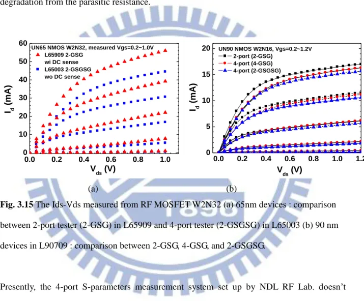
Fig. 3.14 The schematics of 4-port equivalent circuit incorporating parasitic resistances from off-chip DC cables and on-chip interconnection lines. ... 34 Fig. 3.15 The Ids-Vds measured from RF MOSFET W2N32 (a) 65nm devices : comparison between 2-port tester (2-GSG) in L65909 and 4-port tester (2-GSGSG) in L65003 (b) 90 nm devices in L90709 : comparison between 2-GSG, 4-GSG, and 2-GSGSG. ... 35 Fig. 3.16 Comparison of the measured and simulated Ids-Vds under various Vgs (0.2~1.0V) for
4-port RF NMOS W2N32 (65 nm L65003). Parasitic resistances at 4 terminals, Rs=Rd=Rg=Rb=2Ω were employed for I-V simulation ... 36 Fig. 3.17 Comparison of simulated gm-Vgs at Vds=1.0V for 4-port RF NMOS W2N32 (65 nm
L65003) under three conditions : I-V characteristics, Y-parameter without DC cable resistance, and Y-parameters with DC cable resistance. ... 38 Fig. 3.18 (a) Substrate network modeled by a single resistor. [5]-[6] (b) T-type substrate network [13],[15]. (c) Ω-type substrate network. [8], [14] (d) RC parallel substrate network. [11]-[12] (e) substrate network in [16]. (f) The schematic diagram of body network and substrate network. ... 42 Fig. 3.19 The cross section of 4T MOSFET with deep n-well tied together with p-well body and connected with port-4. ... 47 Fig. 3.20 A new body network model proposed for UN65 4-port MOSFET (L65003) in which the deep n-well (DNW) and p-well body (B) are tied together to port-4, and P-sub is connected to ground ... 47 Fig. 3.21 Re(Z44)=Re(Zsub) measured from port-4 (body) with all the other 3 ports (1 : G, 2 : D,
3 : S) at open state and under various body biases : ZBB (Vbs=0), FBB (Vbs=0.6V), and
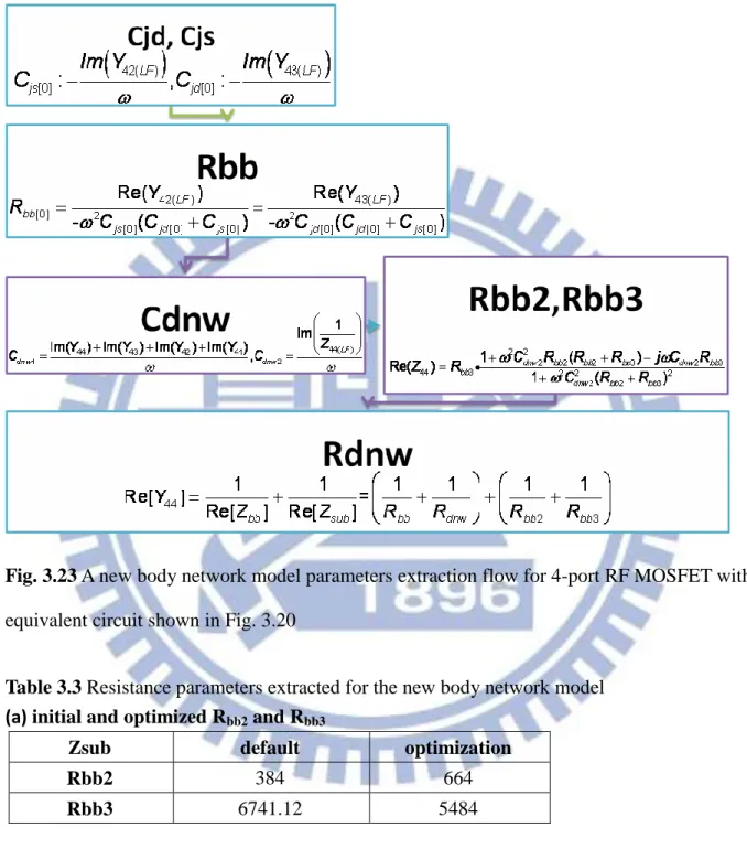
RBB(Vbs=-0.6V). ... 48 Fig. 3.22 Step by step synthesis of body network model (a) substrate network for deep n-well/p-substrate (b) p-well body network for p-well/deep n-well and substrate for deep n-well/p-substrate (c) a complete body network model for L65003 4T RFMOSFET ... 48 Fig. 3.23 A new body network model parameters extraction flow for 4-port RF MOSFET with equivalent circuit shown in Fig. 3.20 ... 49 Fig. 3.24 Comparison of measured and simulated Re(Y44) using the new body network model
and extracted parameters under ZBB (Vbs=0), FBB (Vbs=0.6V), and RBB(Vbs=-0.6V). ... 50 Fig. 3.25 The gate to body capacitances measured from 4-port Y-parameters after openM3 deembedding on 4-port RF MOSFET –Im(Y14)/=Cgb=Cgb1+Cgb2 ... 51 Fig. 3.26 RF MOSFET layout remarked with poly gate fingers, gate contact and metal to contacts, body contacts and metal to contacts. The metals to gate contacts and body contacts will contribute inter-metal coupling capacitance. ... 51 Fig. 3.27 4-port MOSFET device cross section and the representation of RC elements for the equivalent circuit at off state Vgs=Vds=Vbs =0 ... 56 Fig. 3.28 Small signal equivalent circuit with new body network model for 4-port RF
XI
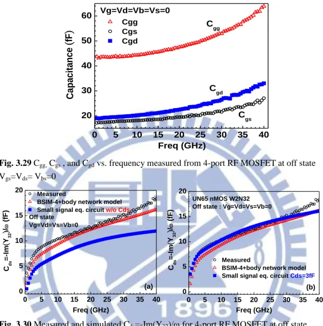
MOSFET at off state Vgs=Vds= Vbs=0 ... 56 Fig. 3.29 Cgg, Cgs , and Cgd vs. frequency measured from 4-port RF MOSFET at off state
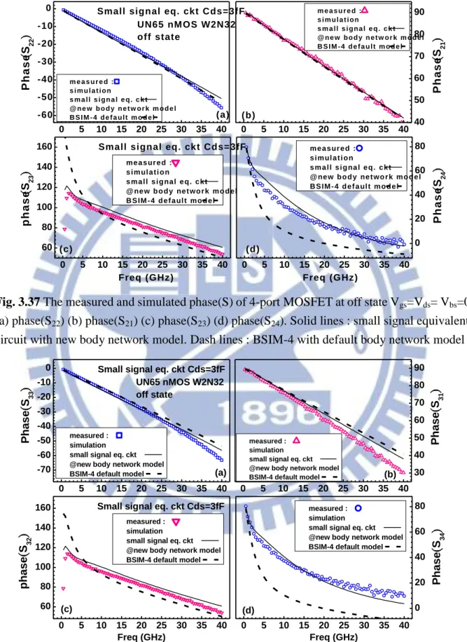
Vgs=Vds= Vbs=0 ... 57 Fig. 3.30 Measured and simulated Cds=-Im(Y32)/ for 4-port RF MOSFET at off state
Vgs=Vds= Vbs=0. Simulation using BSIM-4 and small signal equivalent circuit (a) without
extrinsic Cds (b) with extrinsic Cds =3fF ... 57 Fig. 3.31 The measured and simulated Mag(S) of Dual gate at off state Vgs=Vds= Vbs=0 (a)
Mag(S44) (b) Mag(S41) (c) Mag(S42) (d) Mag(S43). Solid lines : small signal equivalent circuit
with body network model. ... 58 Fig. 3.32 The measured and simulated Mag(S) of Dual gate at off state Vgs=Vds= Vbs=0 (a)
Mag(S11) (b) Mag(S12) (c) Mag(S13) (d) Mag(S14). Solid lines : small signal equivalent circuit
with new body network model. Dash lines : BSIM-4 with default body network model ... 58 Fig. 3.33 The measured and simulated Mag(S) of 4-port MOSFET at off state Vgs=Vds= Vbs=0
(a) Mag(S22) (b) Mag(S21) (c) Mag(S23) (d) Mag(S24). Solid lines : small signal equivalent
circuit with new body network model. Dash lines : BSIM-4 with default body network model ... 59 Fig. 3.34 The measured and simulated Mag(S) of 4-port MOSFET at off state Vgs=Vds= Vbs=0
(a) Mag(S33) (b) Mag(S31) (c) Mag(S32) (d) Mag(S34). Solid lines : small signal equivalent
circuit with new body network model. Dash lines : BSIM-4 with default body network model ... 59 Fig. 3.35 The measured and simulated phase(S) of 4-port MOSFET at off state Vgs=Vds= Vbs=0
(a) phase(S44) (b) phase(S41) (c) phase(S42) (d) phase(S43). Solid lines : small signal equivalent
circuit with new body network model. Dash lines : BSIM-4 with default body network model ... 60 Fig. 3.36 The measured and simulated phase(S) of 4-port MOSFET at off state Vgs=Vds= Vbs=0 (a) phase(S11) (b) phase(S12) (c) phase(S13) (d) phase(S14). Solid lines : small signal equivalent circuit with new body network model. Dash lines : BSIM-4 with default body network model. ... 60 Fig. 3.37 The measured and simulated phase(S) of 4-port MOSFET at off state Vgs=Vds= Vbs=0
(a) phase(S22) (b) phase(S21) (c) phase(S23) (d) phase(S24). Solid lines : small signal equivalent
circuit with new body network model. Dash lines : BSIM-4 with default body network model ... 61 Fig. 3.38 The measured and simulated phase(S) of 4-port MOSFET at off state Vgs=Vds= Vbs=0
(a) phase(S33) (b) phase(S31) (c) phaseS32) (d) phase(S34). Solid lines : small signal equivalent
circuit with new body network model. Dash lines : BSIM-4 with default body network model ... 61 Fig. 3.39 Measured and simulated Re(Y42) and Re(Y43) for 4-port MOSFET at off state
XII
Solid lines : with new body network model. Dash lines : with default body network model .. 62 Fig. 3.40 Measured and simulated Re(Y42) and Re(Y43) for 4-port MOSFET at off state
Vgs=Vds= Vbs=0 (a) Re(Y42) (b) Re(Y43). Simulation by BSIM-4, solid lines : with new body
network model, dash lines : with default body network model ... 62 Fig. 3.41 Measured and simulated Re(Y33) for 4-port MOSFET at off state Vgs=Vds= Vbs=0 (a)
simulation by small signal equivalent circuit (b) simulation by BSIM-4. Solid lines : with new body network model. Dash lines : with default body network model ... 62 Fig. 3.42 4-port MOSFET device cross section and the representation of RC elements for the small signal equivalent circuit in linear region, Vgs=1.0V, Vds=Vbs =0 ... 64 Fig. 3.43 Small signal equivalent circuit with new body network model for 4-port RF MOSFET in linear region, Vgs=1.0V, Vds= Vbs=0. Rch represents channel resistance of the
inversion channel. ... 64 Fig. 3.44 Im(Y11)/, -Im(Y12)/, and -Im(Y13)/ vs. frequency measured from 4-port RF
MOSFET under the biases in linear region Vgs=1.0V, Vds=Vbs=0. Cgg, Cgs, and Cgd determined
from Im(Y11)/, -Im(Y12)/, and -Im(Y13)/ at very low frequency ... 65 Fig. 3.45 The measured and simulated Mag(S) of 4-port MOSFET in linear region Vgs=1.0V,
Vds=Vbs=0 (a) Mag(S44) (b) Mag(S41) (c) Mag(S42) (d) Mag(S43). Solid lines : small signal
equivalent circuit with new body network model. Dash lines : BSIM-4 with default body network model. ... 67 Fig. 3.46 The measured and simulated Mag(S) of 4-port MOSFET in linear region Vgs=1.0V,
Vds=Vbs=0 (a) Mag(S11) (b) Mag(S12) (c) Mag(S13) (d) Mag(S14). Solid lines : small signal
equivalent circuit with new body network model. Dash lines : BSIM-4 with default body network model ... 67 Fig. 3.47 The measured and simulated Mag(S) of 4-port MOSFET in linear region Vgs=1.0V,
Vds=Vbs=0 (a) Mag(S22) (b) Mag(S21) (c) Mag(S23) (d) Mag(S24). Solid lines : small signal
equivalent circuit with new body network model. Dash lines : BSIM-4 with default body network model ... 68 Fig. 3.48 The measured and simulated Mag(S) of 4-port MOSFET in linear region Vgs=1.0V,
Vds=Vbs=0 (a) Mag(S33) (b) Mag(S31) (c) Mag(S32) (d) Mag(S34). Solid lines : small signal
equivalent circuit with new body network model. Dash lines : BSIM-4 with default body network model ... 68 Fig. 3.49 The measured and simulated phase(S) of 4-port MOSFET in linear region Vgs=1.0V,
Vds=Vbs=0 (a) phase(S44) (b) phase(S41) (c) phase(S42) (d) phase(S43). Solid lines : small
signal equivalent circuit with new body network model. Dash lines : BSIM-4 with default body network model ... 69 Fig. 3.50 The measured and simulated phase(S) of 4-port MOSFET in linear region Vgs=1.0V,
Vds=Vbs=0 (a) phase(S11) (b) phase(S12) (c) phase(S13) (d) phase(S14). Solid lines : small signal
XIII
network model ... 69 Fig. 3.51 The measured and simulated phase(S) of 4-port MOSFET in linear region Vgs=1.0V,
Vds=Vbs=0 (a) phase(S22) (b) phase(S21) (c) phase(S23) (d) phase(S24). Solid lines : small
signal equivalent circuit with new body network model. Dash lines : BSIM-4 with default body network model ... 70 Fig. 3.52 The measured and simulated phase(S) of 4-port MOSFET in linear region Vgs=1.0V,
Vds=Vbs=0 (a) phase(S33) (b) phase(S31) (c) phaseS32) (d) phase(S34). Solid lines : small signal
equivalent circuit with new body network model. Dash lines : BSIM-4 with default body network model ... 70 Fig. 3.53 Measured and simulated Re(Y42) and Re(Y43) for 4-port MOSFET in linear region
Vgs=1.0V, Vds=Vbs=0 (a) Re(Y42) (b) Re(Y43). Simulation by small signal equivalent circuit
model. Solid lines : new body network model. Dash lines : default body network model ... 71 Fig. 3.54 Measured and simulated Re(Y42) and Re(Y43) for 4-port MOSFET in linear region
Vgs=1.0V, Vds=Vbs=0 (a) Re(Y42) (b) Re(Y43). Simulation by BSIM-4, solid lines : with new
body network model. Dash lines : with default body network model ... 71 Fig. 3.55 Measured and simulated Re(Y33) for 4-port MOSFET in linear region Vgs=1.0V,
Vds=Vbs=0 (a) simulation by small signal equivalent circuit (b) simulation by BSIM-4. Solid
lines : with new body network model. Dash lines : with default body network model ... 71 Fig. 3.56 A small signal equivalent circuit for 4-port RF MOSFET in saturation region. gm, gmb,
and ro are deployed to simulate conduction channel under saturation condition... 73 Fig. 3.57 Im(Y11)/, -Im(Y12)/, and -Im(Y13)/ vs. frequency measured from 4-port RF
MOSFET in saturation region, Vgs=0.8V, Vds=1.0V, Vbs=0. Cgg, Cgs, and Cgd determined from
Im(Y11)/, -Im(Y12)/, and -Im(Y13)/ at very low frequency... 73 Fig. 3.58 Iteration flow chart for the extraction of gm, gmb, ro, and Rs in 4T RF MOSFETs 74 Fig. 3.59 The measured and simulated Mag(S) of 4-port MOSFET in saturation region Vgs=0.8V, Vds=1V, Vbs=0 (a) Mag(S44) (b) Mag(S41) (c) Mag(S42) (d) Mag(S43). Solid lines :
small signal equivalent circuit with new body network model. Dash lines : BSIM-4 with default body network model. ... 79 Fig. 3.60 The measured and simulated Mag(S) of 4-port MOSFET in saturation region Vgs=0.8V, Vds=1V, Vbs=0 (a) Mag(S11) (b) Mag(S12) (c) Mag(S13) (d) Mag(S14). Solid lines :
small signal equivalent circuit with new body network model. Dash lines : BSIM-4 with default body network model. ... 79 Fig. 3.61 The measured and simulated Mag(S) of 4-port MOSFET in saturation region Vgs=0.8V, Vds=1V, Vbs=0 (a) Mag(S22) (b) Mag(S21) (c) Mag(S23) (d) Mag(S24). Solid lines :
small signal equivalent circuit with new body network model. Dash lines : BSIM-4 with default body network model. ... 80 Fig. 3.62 The measured and simulated Mag(S) of 4-port MOSFET in saturation region Vgs=0.8V, Vds=1V, Vbs=0 (a) Mag(S33) (b) Mag(S31) (c) Mag(S32) (d) Mag(S34). Solid lines :
XIV
small signal equivalent circuit with new body network model. Dash lines : BSIM-4 with default body network model. ... 80 Fig. 3.63 The measured and simulated phase(S) of 4-port MOSFET in saturation region Vgs=0.8V, Vds=1V, Vbs=0 (a) phase(S44) (b) phase(S41) (c) phase(S42) (d) phase(S43). Solid
lines : small signal equivalent circuit with new body network model. Dash lines : BSIM-4 with default body network model. ... 81 Fig. 3.64 The measured and simulated phase(S) of 4-port MOSFET in saturation region Vgs=0.8V, Vds=1V, Vbs=0 (a) phase(S11) (b) phase(S12) (c) phase(S13) (d) phase(S14). Solid
lines : small signal equivalent circuit with new body network model. Dash lines : BSIM-4 with default body network model. ... 81 Fig. 3.65 The measured and simulated phase(S) of 4-port MOSFET in saturation region Vgs=0.8V, Vds=1V, Vbs=0 (a) phase(S22) (b) phase(S21) (c) phase(S23) (d) phase(S24). Solid
lines : small signal equivalent circuit with new body network model. Dash lines : BSIM-4 with default body network model. ... 82 Fig. 3.66 The measured and simulated phase(S) of 4-port MOSFET in saturation region Vgs=0.8V, Vds=1V, Vbs=0 (a) phase(S33) (b) phase(S31) (c) phase(S32) (d) phase(S34). Solid
lines : small signal equivalent circuit with new body network model. Dash lines : BSIM-4 with default body network model. ... 82 Fig. 3.67 Measured and simulated Re(Y42) and Re(Y43) for 4-port MOSFET in saturation
region Vgs=0.8V, Vds=1V, Vbs=0 (a) Re(Y42) (b) Re(Y43). Simulation by small signal
equivalent circuit model. Solid lines : new body network model. Dash lines : default body network model ... 83 Fig. 3.68 Measured and simulated Re(Y42) and Re(Y43) for 4-port MOSFET in saturation
region Vgs=0.8V, Vds=1V, Vbs=0 (a) Re(Y42) (b) Re(Y43). Simulation by BSIM-4. Solid lines :
new body network model. Dash lines : default body network model ... 83 Fig. 3.69 Measured and simulated Re(Y33) for 4-port MOSFET in saturation region Vgs=0.8V,
Vds=1V, Vbs=0 (a) simulation by small signal equivalent circuit (b) simulation by BSIM-4.
Solid lines : with new body network model. Dash lines : with default body network model .. 83 Fig. 3.70 UN65 NMOS W2N32, measured and simulated Ids-Vgs at Vds=0.05V and 1.2V
(a)ZBB : Vbs=0V (b) FBB : Vbs=0.6V (c) RBB : Vbs=-0.6V ... 96 Fig. 3.71 UN65 NMOS W2N32, measured and simulated gm-Vgs at Vd=0.05V and 1.2V
(a)ZBB : Vbs=0V (b) FBB : Vbs=0.6V (c) RBB : Vbs=-0.6V. ... 97 Fig. 3.72 UN65 NMOS W2N32, measured and simulated log(Ids)-Vgs at Vds=0.05V and 1.2V
(a)ZBB : Vbs=0V (b) FBB : Vbs=0.6V (c) RBB : Vbs=-0.6V. ... 98
Fig. 3.73 UN65 NMOS W2N32, measured and simulated Ids-Vds under Vgs gs=
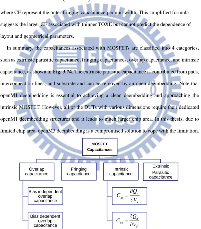
0.2V (a)ZBB : Vbs=0V (b) FBB : Vbs=0.6V (c) RBB : Vbs=-0.6V ... 99 Fig. 3.74 MOSFET capacitances classified into four categories for C-V modeling : extrinsic parasitic capacitance, fringing capacitance, overlap capacitance, and intrinsic capacitance . 110
XV
Fig. 3.75 Small signal equivalent circuit of a standard MOSFET after open deembedding .. 113 Fig. 3.76 The gate related capacitances extracted from 4-port Y-parameters after openM3 deembedding on 4-port RF MOSFET (a) Cgg and Cgs+Cgd+Cgb (b) Cgs and Cgd (c)
Cgb=Cgb1+Cgb2 ... 114 Fig. 3.77 Gate sidewall fringing capacitances, Cof=Cg,Diff+Cg,CT simulated by Raphael for
UN65 n-MOSFET (a) Cof, Cg,Diff, and Cg,CT vs. Lg (b) Cof, Cg,Diff, and Cg,CT vs. Lg,CT (c) Cof,
Cg,Diff, and Cg,CT vs. Tg (d) Cof, Cg,Diff, and Cg,CT vs. Tox ... 115 Fig. 3.78 MOSFET capacitance model parameters extraction flow ... 115 Fig. 3.79 Comparison of measured and simulated gate capacitances under ZBB (Vbs=0) (a) Cgg,
(b) Cgs (c) Cgd and (d) Cgb. Simulation using default C-V model parameters (dash line) and
modified parameters (solid line). ... 116 Fig. 3.80 Comparison of measured and simulated gate capacitances under FBB (Vbs=0.6V) (a)
Cgg, (b) Cgs (c) Cgd and (d) Cgb. Simulation using default C-V model parameters (dash line) and
modified parameters (solid line). ... 117 Fig. 3.81 Comparison of measured and simulated gate capacitances under RBB (Vbs=-0.6V) (a)
Cgg, (b) Cgs (c) Cgd and (d) Cgb. Simulation using default C-V model parameters (dash line) and
modified parameters (solid line). ... 118 Fig. 3.82 Measured and simulated gm versus Vgs for 4-port MOSFET under Vds=1.2V and
dynamic body biases. ZBB: Vbs=0, FBB: Vbs=0.6V, RBB: Vbs=-0.6V. Simulation : BSIM-4
with new body netowork model. ... 119 Fig. 3.83 Measured and simulated gm versus Vgs for 4-port MOSFET under Vds=1.0V and
dynamic body biases. ZBB: Vbs=0, FBB: Vbs=0.6V, RBB: Vbs=-0.6V. Simulation : BSIM-4
with new body netowork model. ... 120 Fig. 3.84 Measured and simulated fT versus Vgs for 4-port MOSFET under Vds=1.0V and
dynamic body biases. ZBB: Vbs=0, FBB: Vbs=0.6V, RBB: Vbs=-0.6V. Simulation : BSIM-4
with new body netowork model. ... 120 Fig. 4.1 A cascode amplifier with a common source amplifier as the input stage driven by signal source Vin. ... 121 Fig. 4.2 The illustration of cascode layouts (a) conventional cascode with two separate MOSFETs (b) new cascode with dual-gate MOSFET and merged source/drain ... 128 Fig. 4.3 The layouts of 2-port and 4-port test structures for RF MOSFET measurement (a) 2-port tester with two GSG pads in parallel (b) 4-port tester, namely 4-GSG with four GSG pads in perpendicular direction between every two adjacent pads (c) 4-port tester, namely 2-GSGSG with two GSGSG pads in parallel. ... 131 Fig. 4.4 The equivalent circuit for a four-port test structure incorporating parasitic impedances (Zs) and admittances (Ypad, Yps) ... 132 Fig. 4.5 The parasitic resistance extracted from two-port (2-GSG ) and four-port (2-GSGSG, 4-GSG) shortM3 deembedding structures (a) Rg and Rd for interconnection lines to gate and
XVI
drain pads (b)Rs and Rb for interconnection lines to source and body pads ... 132 Fig. 4.6 The parasitic inductances extracted from two-port (2-GSG ) and four-port (2-GSGSG, 4-GSG) shortM3 deembedding structures (a) Lg and Ld for interconnection lines to gate and
drain pads (b) Ls and Lb for interconnection lines to source and body pads ... 133 Fig. 4.7 Simplified circuit schematics for (a) dual-gate MOSFET with 4-port assignment as G1 (1), S(2), D(3), G2(4), and body connected to ground (b) common gate structure with G1 and G2 shorted together to port-1 and body to port-4, resulting 4-port assignment : G1/G2 (1), S (2), D(3), and B(4). ... 135 Fig. 4.8 (a) The circuit schematics of dual-gate MOSFET with a detailed assignment of the capacitive, inductive, and resistive components (b) layout of the dual-gate MOSFET ... 135 Fig. 4.9 The small signal equivalent circuit model of dual-gate MOSFET at off state : the region remarked by solid-line box is the intrinsic device model excluding body network model and the region enclosed by dash-line box is the body network model ... 138 Fig. 4.10 Model parameters extraction flow for small signal equivalent circuit model of dual-gate MOSFET at off state (VG1= VG2= VD= VS= VB=0) ... 139 Fig. 4.11 The in-stage gate capacitances Cg1s and Cg2d extracted from Im(YG1S) and Im(YG2D)
of dual-gate MOSFET at off state. Cgs and Cgd of the standard MOSFET (W2N32) are
provided for a comparison. ... 142 Fig. 4.12 The cross-stage gate capacitances Cg1d and Cg2s extracted from Im(YG1D) and
Im(YG2S) of dual-gate MOSFET at off state. In-stage capacitance Cg1s and Cg2d of the same
device are provided for a comparison. ... 143 Fig. 4.13 The cross-stage gate capacitances Cg1d and Cg2s extracted from Im(YG1D) and
Im(YG2S) of dual-gate MOSFET at off state. The total gate capacitances Cgg1 and Cgg2
associated with G1 and G2 of this dual-gate MOSFET are provided for a comparison. ... 143 Fig. 4.14 The inter-gate capacitances Cg1g2 extracted from Im(YG1G2) of dual-gate MOSFET at
off state (VG1= VG2= VD= VS= VB=0). ... 144 Fig. 4.15 The inter-stage gate capacitances Cg1d1 and Cg2s2 calculated by (4.13) and (4.14) with
all of the other gate capacitances extracted from (4.5)~(4.12) for dual-gate MOSFET at off state. In-stage capacitance Cg1s and Cg2d of the same device are provided for a comparison. 144 Fig. 4.16 The gate to body capacitance Cgb extracted from Im(YGB) of common gate cascode
structure at off state(VG= VD= VS= VB=0) and the comparion with Cgb measured the standard
MOSFET (W2N32). ... 145 Fig. 4.17 The layout of dual-gate MOSFET with the layers remarked for the contacts to gate, drain, body, and deep n-well (DNW). Cgb can be contributed from the inter-metal coupling
capacitance : metal-3 (M3) on the gate contacts to metal-4 (M4) on body contacts. ... 145 Fig. 4.18 The junction capacitances Cjs and Cjd extracted from Im(YBS) and Im(YBS) of
common gate cascode structure at off state. ... 146 Fig. 4.19 The comparison of total gate capacitances measured from dual-gate MOSFET (Cgg1
XVII
+Cgg2), common gate MOSFET (Cgg_CG) and single MOSFET at off state. ... 146 Fig. 4.20 The comparison between the extracted in-stage gate capacitances Cg1s and Cg2d and
those simulated with and without parasitic inductances (a) simulation with Lg=Ld =Ls=Lb
=70pH (b) simulation without inductance. ... 147 Fig. 4.21 The gate resistances of a dual-gate MOSFET (a) Rg1 and Rg2 extracted by
Y-method (b) the comparison with simulation (BSIM4). ... 147 Fig. 4.22 The measured and simulated Mag(S) of dual-gate MOSFET at off state VG1=
VG2=VD= VS= VB=0 (a) Mag(S11) (b) Mag(S12) (c) Mag(S13) (d) Mag(S14). Symbols :
measurement. Lines : simulation by small signal equivalent circuit with body network model. ... 149 Fig. 4.23 The measured and simulated Mag(S) of dual-gate MOSFET at off state VG1=
VG2=VD= VS= VB=0 (a) Mag(S44) (b) Mag(S41) (c) Mag(S42) (d) Mag(S43). Symbols :
measurement. Lines : simulation by small signal equivalent circuit with body network model. ... 149 Fig. 4.24 The measured and simulated Mag(S) of dual-gate MOSFET at off state VG1=
VG2=VD= VS= VB=0 (a) Mag(S33) (b) Mag(S32) (c) Mag(S31) (d) Mag(S34). Symbols :
measurement. Lines : simulation by small signal equivalent circuit with body network model. ... 150 Fig. 4.25 The measured and simulated Mag(S) of dual-gate MOSFET at off state VG1=
VG2=VD= VS= VB=0 (a) Mag(S22) (b) Mag(S23) (c) Mag(S21) (d) Mag(S24). Symbols :
measurement. Lines : simulation by small signal equivalent circuit with body network model. ... 150 Fig. 4.26 The measured and simulated phase(S) of dual-gate MOSFET at off state VG1=
VG2=VD= VS= VB=0 (a) phase(S11) (b) phase(S12) (c) phase(S13) (d) phase(S14). Symbols :
measurement. Lines : simulation by small signal equivalent circuit with body network model. ... 151 Fig. 4.27 The measured and simulated phase(S) of dual-gate MOSFET at off state VG1=
VG2=VD= VS= VB=0 (a) phase(S44) (b) phase(S41) (c) phase(S42) (d) phase(S43). Symbols :
measurement. Lines : simulation by small signal equivalent circuit with body network model. ... 151 Fig. 4.28 The measured and simulated phase(S) of dual-gate MOSFET at off state VG1=
VG2=VD= VS= VB=0 (a) phase(S33) (b) phase(S31) (c) phase(S32) (d) phase(S34). Symbols :
measurement. Lines : simulation by small signal equivalent circuit with body network model. ... 152 Fig. 4.29 The measured and simulated phase(S) of dual-gate MOSFET at off state VG1=
VG2=VD= VS= VB=0 (a) phase(S22) (b) phase(S24) (c) phase(S23) (d) phase(S21). Symbols :
measurement. Lines : simulation by small signal equivalent circuit with body network model. ... 152
XVIII
Fig. 4.30 The small signal equivalent circuit model of dual-gate MOSFET at active state. M1 and M2 are operated at saturation mode and the channel conduction is modeled by gm1 and ro1
for M1 and gm2 and ro2 for M2. ... 156 Fig. 4.31 Model parameters extraction flow for small signal equivalent circuit model of dual-gate MOSFET at active state ... 157 Fig. 4.32 The comparison of measurement and simulation for dual-gate MOSFET at active state VG1=0.4V, VG2=0.6V, VD=1.0V, VS= VB=0 (a) Gm=Re(Y31) (b) Rout=1/Re(Y33) (c)
Mag(S31) (d) Mag(S33). Symbols : measurement. Lines : simulation by small signal equivalent
circuit with body network model. ... 158 Fig. 4.33 The measured and simulated Mag(S) of dual-gate MOSFET at active state VG1=0.4V,
VG22=0.6V VD=1.0V (a) Mag(S11) (b) Mag(S12) (c) Mag(S13) (d) Mag(S14). Symbols : measurement. Lines : simulation by small signal equivalent circuit with body network model. ... 159 Fig. 4.34 The measured and simulated Mag(S) of dual-gate MOSFET at active state VG1=0.4V,
VG22=0.6V VD=1.0V (a) Mag(S44) (b) Mag(S41) (c) Mag(S42) (d) Mag(S43). Symbols : measurement. Lines : simulation by small signal equivalent circuit with body network model. ... 159 Fig. 4.35 The measured and simulated Mag(S) of dual-gate MOSFET at active state VG1=0.4V,
VG22=0.6V VD=1.0V (a) Mag(S33) (b) Mag(S32) (c) Mag(S31) (d) Mag(S34). Symbols : measurement. Lines : simulation by small signal equivalent circuit with body network model. ... 160 Fig. 4.36 The measured and simulated Mag(S) of dual-gate MOSFET at active state VG1=0.4V,
VG22=0.6V VD=1.0V (a) Mag(S22) (b) Mag(S23) (c) Mag(S21) (d) Mag(S24). Symbols : measurement. Lines : simulation by small signal equivalent circuit with body network model. ... 160 Fig. 4.37 The measured and simulated phase(S) of dual-gate MOSFET at active state VG1=0.4V,
VG22=0.6V VD=1.0V (a) phase(S11) (b) phase(S12) (c) phase(S13) (d) phase(S14). Symbols : measurement. Lines : simulation by small signal equivalent circuit with body network model. ... 161 Fig. 4.38 The measured and simulated phase(S) of dual-gate MOSFET at active state VG1=0.4V,
VG22=0.6V VD=1.0V (a) phase(S44) (b) phase(S41) (c) phase(S42) (d) phase(S43). Symbols : measurement. Lines : simulation by small signal equivalent circuit with body network model. ... 161 Fig. 4.39 The measured and simulated phase(S) of dual-gate MOSFET at active state VG1=0.4V,
VG22=0.6V VD=1.0V (a) phase(S33) (b) phase(S31) (c) phase(S32) (d) phase(S34). Symbols : measurement. Lines : simulation by small signal equivalent circuit with body network model. ... 162 Fig. 4.40 The measured and simulated phase(S) of dual-gate MOSFET at active state VG1=0.4V,
XIX
VG22=0.6V VD=1.0V (a) phase(S22) (b) phase(S24) (c) phase(S23) (d) phase(S21). Symbols : measurement. Lines : simulation by small signal equivalent circuit with body network model. ... 162 Fig. 4.41 The equivalent circuit schematics built in BSIM-4 for dual-gate MOSFET simulation ... 164 Fig. 4.42 The measured and simulate IDS-VDS of dual-gate MOSFET under VG2=1.0V and
varying VG1=0.2~1.2V. Rg1= Rg2= Rd= Rs=1 for 4 terminals, Rds,diff=1 for merged S/D
region. Symbols : measurement. Lines : BSIM-4 simulation. ... 166 Fig. 4.43 The measured and simulate IDS-VDS of dual-gate MOSFET (a) VG2=1.0V,
VG1=0.2~1.2V (b) VG1=1.0V, VG2=0.2~1.0V. Rg1= Rg2= Rd= Rs=1 for 4 terminals, Rds,diff=1
for merged S/D region. Symbols : measurement. Lines : BSIM-4 simulation. ... 166 Fig. 4.44 The measured and simulate IDS-VDS of dual-gate MOSFET (a) VG2=0.6V,
VG1=0.2~1.0V (b) VG1=0.6V, VG2=0.2~1.0V. Rg1= Rg2= Rd= Rs=1 for 4 terminals, Rds,diff=1
for merged S/D region. Symbols : measurement. Lines : BSIM-4 simulation. ... 167 Fig. 4.45 The measured and simulated gate capacitances : in-stage, cross-stage, and total gate capacitances of dual-gate MOSFET. Symbols : measurement. Lines :BSIM-4 simulation. .. 168 Fig. 4.46 The comparison between measurement and BSIM-4 simulation (a) Gm (b) H21, (c)
maximum available gain (MAG) and (d) Unilateral gain of dual-gate MOSFET at active state VG1=0.4V, VG22=0.6V VD=1.0V ... 169 Fig. 4.47 The measured and simulated mag(S) of dual-gate MOSFET at off state VG1=
VG2=VD= VS= VB=0 (a) Mag(S11) (b) Mag(S12) (c) Mag(S13) (d) Mag(S14). Symbols :
measurement. Solid lines : BSIM4 simulation. ... 170 Fig. 4.48 The measured and simulated mag(S) of dual-gate MOSFET at off state VG1=
VG2=VD= VS= VB=0 (a) Mag(S44) (b) Mag(S41) (c) Mag(S42) (d) Mag(S43). Symbols :
measurement. Solid lines : BSIM4 simulation. ... 170 Fig. 4.49 The measured and simulated mag(S) of dual-gate MOSFET at off state VG1=
VG2=VD= VS= VB=0 (a) Mag(S33) (b) Mag(S32) (c) Mag(S31) (d) Mag(S34). Symbols :
measurement. Solid lines : BSIM4 simulation. ... 171 Fig. 4.50 The measured and simulated mag(S) of dual-gate MOSFET at off state VG1=
VG2=VD= VS= VB=0 (a) Mag(S22) (b) Mag(S23) (c) Mag(S21) (d) Mag(S24). Symbols :
measurement. Solid lines : BSIM4 simulation. ... 171 Fig. 4.51 The measured and simulated phase(S) of dual-gate MOSFET at off state VG1=
VG2=VD= VS= VB=0 (a) phase(S44) (b) phase(S41) (c) phase(S42) (d) phase(S43). Symbols :
measurement. Solid lines : BSIM4 simulation. ... 172 Fig. 4.52 The measured and simulated phase(S) of dual-gate MOSFET at off state VG1=
VG2=VD= VS= VB=0 (a) phase(S11) (b) phase(S12) (c) phase(S13) (d) phase(S14). Symbols :
measurement. Solid lines : BSIM4 simulation. ... 172 Fig. 4.53 The measured and simulated phase(S) of dual-gate MOSFET at off state VG1=
XX
VG2=VD= VS= VB=0 (a) phase(S33) (b) phase(S31) (c) phase(S32) (d) phase(S34). Symbols :
measurement. Solid lines : BSIM4 simulation. ... 173 Fig. 4.54 The measured and simulated phase(S) of dual-gate MOSFET at off state VG1=
VG2=VD= VS= VB=0 (a) phase(S22) (b) phase(S24) (c) phase(S23) (d) phase(S21). Symbols :
measurement. Solid lines : BSIM4 simulation. ... 173 Fig. 4.55 The measured and simulated mag(S) of dual-gate MOSFET at active state VG1=0.4V,
VG22=0.6V VD=1.0V (a) Mag(S11) (b) Mag(S12) (c) Mag(S13) (d) Mag(S14). Symbols : measurement. Solid lines : BSIM4 simulation. ... 174 Fig. 4.56 The measured and simulated mag(S) of dual-gate MOSFET at active state VG1=0.4V,
VG22=0.6V VD=1.0V (a) Mag(S44) (b) Mag(S41) (c) Mag(S42) (d) Mag(S43). Symbols : measurement. Solid lines : BSIM4 simulation. ... 174 Fig. 4.57 The measured and simulated mag(S) of dual-gate MOSFET at active state VG1=0.4V,
VG22=0.6V VD=1.0V (a) Mag(S33) (b) Mag(S32) (c) Mag(S31) (d) Mag(S34). Symbols : measurement. Solid lines : BSIM4 simulation. ... 175 Fig. 4.58 The measured and simulated mag(S) of dual-gate MOSFET at active state VG1=0.4V,
VG22=0.6V VD=1.0V (a) Mag(S22) (b) Mag(S23) (c) Mag(S21) (d) Mag(S24). Symbols : measurement. Solid lines : BSIM4 simulation. ... 175 Fig. 4.59 The measured and simulated phase(S) of dual-gate MOSFET at active state VG1=0.4V,
VG22=0.6V VD=1.0V (a) phase(S33) (b) phase(S31) (c) phase(S32) (d) phase(S34). Symbols : measurement. Solid lines : BSIM4 simulation. ... 176 Fig. 4.60 The measured and simulated phase(S) of dual-gate MOSFET at active state VG1=0.4V,
VG22=0.6V VD=1.0V (a) phase(S44) (b) phase(S41) (c) phase(S42) (d) phase(S43). Symbols : measurement. Solid lines : BSIM4 simulation. ... 176 Fig. 4.61 The measured and simulated phase(S) of dual-gate MOSFET at active state VG1=0.4V,
VG22=0.6V VD=1.0V (a) phase(S22) (b) phase(S24) (c) phase(S23) (d) phase(S21). Symbols : measurement. Solid lines : BSIM4 simulation. ... 177 Fig. 4.62 The measured and simulated phase(S) of dual-gate MOSFET at active state VG1=0.4V,
VG22=0.6V VD=1.0V (a) phase(S11) (b) phase(S12) (c) phase(S13) (d) phase(S14). Symbols : measurement. Solid lines : BSIM4 simulation. ... 177
XXI
Table Caption
Table 3.1 (a) 4T RF MOSFET layouts in test chips using different processes ... 23 Table 3.2 The configurations for DC I-V measurement, 2-port and 4-port S-parameters measurement ... 36 Table 3.3 Resistance parameters extracted for the new body network model ... 49 Table 3.4 Small signal equivalent circuit model parameters of 4-port MOSFET at off state .. 57 Table 3.5 Small signal equivalent circuit model parameters of 4-port MOSFET in linear region (Vgs=1.0V, Vds= Vbs=0) ... 65 Table 3.6 Iteration flow for gm and gmb extraction and optimization ... 76 Table 3.7 Small signal equivalent circuit model parameters of 4-port MOSFET in saturation region (Vgs=0.8V, Vds=1.0V, Vbs=0) ... 77 Table 3.8 (a)VT and mobility models parameters extracted from UN65 MOSFET W2N32
under ZBB ((Vbs=0), FBB ((Vbs=0.6V), and RBB ((Vbs=-0.6V) (b) VT extraction result ... 94 Table 3.9 BSIM-4 capacitance model pptions and matching with BSIM-3.3.2 options ... 101 Table 3.10 Geometrical parameters extracted from UN65 multi-finger MOSFET for I-V and C-V simulation ... 103 Table 3.11 C-V model parameters for UN65 n-MOSFET under ZBB, FBB, and RBB, and a comparison with default parameters ... 116 Table 4.1 Cascode MOSFET operation modes and features... 123 Table 4.2 Comparison between conventional cascode and new casode in various features .. 128 Table 4.3 A complete set of small signal equivalent circuit model parameters of dual-gate MOSFET at off state ... 148 Table 4.4 A complete set of small signal equivalent circuit model parameters of dual-gate MOSFET at active state(VG1=0.4V, VG2=0.6V, VD=1.0V, and VS=VB=0) ... 157 Table 4.5 The equivalent circuit model parameters of dual-gate MOSFET set up in BSIM-4 for I-V, C-V, and high frequency simulation ... 165
1
Chapter 1
Introduction
1.1 An Overview and Motivation
Four-port (4-port) RF MOSFET appears as the basic building block to implement new biasing schemes. The dynamic body biases method has been recognized as one of the best approaches adapted to nanoscale CMOS device and circuit design in trade-off between the active and standby power. New circuit topologies for low power and low noise can be created on the RF/MS CMOS platform, with added features and freedom of DC/RF signal supply enabled by 4-terminal (4T) MOSFETs. Unfortunately, the existing RF CMOS models established by conventional 2-port test structures are valid only for 3T MOSFETs, which are restricted to zero body biases (ZBB) scheme. In addition, the 3T MOSFETs are limited to a common source (CS) topology. Even though CS topology can fit many RF and analog circuits design, common gate (CG) are frequently required for RF and analog circuits, e.g. CG for low power receiver design and for transimpedance amplifier. However, most of the characterization and model development stay with 3T MOSFETs residing on 2-port test structures, due to the relative simplicity compared with 4T MOSFETs in 4-port testers. To solve the mentioned problems and limitations exposed in previous work, extensive research effort has been focused on 4-port test structures design, measurement, de-embedding methods, and body network model development for 4T RF MOSFET modeling. The ultimate goal is to establish a comprehensive 4-port MOSFET model, which can ensure simulation accuracy for RF circuits design adopting dynamic body biases scheme.
In recent two decades, substrate network model becomes an important topic in the area of RF CMOS and different models have been published. However, most of the works have been focused on some minor modifications on the simplest model, i.e. single resistor model. Substrate network model is not available in BSIM-3 and it allows the freedom of deploying
2
different external networks. A -type substrate network with 4 bulk resistors was proposed as a direct extension to BSIM-3 to improve simulation accuracy of output characteristics, such as S22 and Rout at high frequencies. However, this-type substrate network model requires an
extensive modification to BSIM-3 and makes the parameters extraction more complicated. A simplified lumped resistance model with 3 resistors (one gate resistor and two substrate resistors) was proposed to reduce the complexity in parameters extraction and maintain the simulation accuracy for both RF and baseband circuits. As for BSIM-4, an internally built substrate network with 5 resistors is a modified version, trying to enhance the simulation accuracy. Substrate network models with parallel RC instead of simple resistance network were proposed to improve modeling accuracy at high frequency. In summary, the trade-off between the curve fitting capability and difficulty in parameters extraction becomes one of the major limitations.
The mentioned problems and challenges motivate our interest in this research topic. A new body network model is developed in this thesis, based on 4-port RF MOSFETs built with deep n-well on p-substrate and the measured 4-port S-parameters. Note that body network model instead of substrate network model is named in this thesis, to make a clear definition that p-well body is separated from p-substrate by the deep n-well surrounding the p-well body. Furthermore, dual gate MOSFET with merged source/drain diffusion appears as an interesting structure for new cascode with the advantage of smaller cell size and then smaller parasitic junction capacitances. This new cascode structure introduces one more interesting topic of body network model and small signal equivalent circuit model for RF amplifier simulation and design. Again, 4-port S-parameters measurement is required for dual gate MOSFET characterization and model parameters extraction. The new cascode structure has been fabricated in the first test chip using UN65 process to carry out the mentioned model development and verification.
3
1.2 Thesis Organization
The major objective of this thesis is the development of small signal equivalent circuit models for 4-port RF MOSFET and new cascode structure with different configurations to facilitate RF CMOS circuit simulation and design.
First, chapter 2 addresses the fundamental theory of scattering matrix and parameters and RF amplifier consideration. The former one will cover both 2-port and 4-port networks. The latter one includes impedance matching, gain, noise, linearity, and stability.
In chapter 3, a new body network model is developed for 4-port RF MOSFET fabricated with UN65 process in which the p-well body and deep n-well tied together to one port for body terminal. A complete model parameters extraction flow will be provided with details of the extraction formulas. The proposed body network model and can be easily integrated with intrinsic MOSFET to build a small signal equivalent circuit model. The simulation accuracy will be verified by an extensive comparison with measured 4-port S-parameters up to 40GHz and under different operation conditions, such as off-state, linear region, and saturation. Also, a comparison with simulation by BSIM-4 using default body network has been carried out to explore the problem and solution.
In chapter 4, a small signal equivalent circuit is developed for new cascode structure based on a dual gate MOSFET with merged source/drain diffusion region. A modified body network model is created to match different configurations in deep n-well and p-well body. 4-port S-parameters can facilitate the extraction of complicated model parameters in the dual gate MOSFET, such as in-stage capacitances, inter-stage capacitances, and cross-stage capacitances. The small signal equivalent circuit model built with core model for dual gate MOSFET and modified body network model demonstrates acceptable simulation accuracy at off state and saturation region. BSIM-4 is utilized to approach new cascode structure by incorporating parasitic elements such as inter-stage resistance and capacitances into conventional cascode with two single MOSFETs and enable both small signal and large signal
4
simulations.
5
Chapter 2
Fundamental theory
2.1 Scattering Matrix and Parameters
At microwave frequency the Z, Y and H parameters are very difficult to measure, the reason is that short and open circuits to ac signals are difficult to implement at microwave frequencies, so that, the scattering matrix are used usually in the analysis of two port networks usually.
2.1.1 Two–port network and scattering parameters
Considering the two-port network with incident wave a1 and reflected wave b1 at port1, and incident wave a2 and reflected wave b2 at port 2, the S parameters can be written in matrix form as: 1 1 1 1 2 1 2 2 1 2 2 2
b
S
S
a
b
S
S
a
(2.1)2.1.2 Four –port scattering matrix and parameters
The extension of the formulation to four-port network is simple, the transmission lines are assumed to be lossless with characteristic impedance Z0, and then, we can write the scattering parameters of the four-port in matrix form.
11 12 13 14 1 1 21 22 23 24 2 2 31 32 33 34 3 3 41 42 43 44 4 4
S
S
S
S
b
a
S
S
S
S
b
a
S
S
S
S
b
a
S
S
S
S
b
a
;
b
S a
(2.2)Note that the value of S11 in (2.2) will be different from the value of S11 in a two-port common source configuration. For example, S11 can be arranged form the S matrix in (2.2) as
6 1 11 1
a
2a
3a
40
b
S
a
(2.3) To measure S11, the matched resistive terminations of 50Ω are used at ports 2, 3, and 4, and the ratio b1/a1 is obtained. In a two-port common source configuration, S11 is measured with reference resistance 50Ω at port 2 and source/body grounding. Similarly, the parameters S12, S21, and S22 in four-port S matrix will be different form the parameters in two-port matrix.2.1.3 Port reduction method
Considering a 4-port networks system, the I-V relationship of the extrinsic and intrinsic parameters can be written as a 4X4 Y matrix.
1 1 1 2 1 3 1 4 1 1 21 22 23 24 2 2 31 32 33 34 3 3 41 42 43 44 4 4
Y
Y
Y
Y
I
V
Y
Y
Y
Y
I
V
Y
Y
Y
Y
I
V
Y
Y
Y
Y
I
V
(2.4)According to equation (2.4), grounding a terminal is simply giving the corresponding zero supply voltage, and the remained sub-matrix will be the Y matrix representing the resulting configuration of the MOSFET, therefore, the 4 x 4 matrix of the 4-port networks can be reduced to 3-port or 2-port Y matrix. For example, the common source(CS) configuration is source (port3) and body (port4) grounding, the CS 2-port Y matrix can be obtained by setting the Vs=Vb=0V in the 4-port measurement, in this case, the term of source and body in (2.4) is negligible, the reduced Y matrix can be written as
1 11 12 1 2 21 22 2
I
Y
Y
V
I
Y
Y
V
(2.5)2.2 RF Amplifier Design Consideration
7
matching , gain,noise Inter modulation and linearity.
2.2.1 Impedance matching
Low noise amplifier is the first stage in the receiver front-end circuits and is used to amplify the received weak RF signal with the minimum noise figure. As it is well recognized that impedance matching is the fundamental requirement in LNA designs for achieving the target performance of both gain and noise. There are four basic 50-Ω input matching architectures that have been explored in the traditional transistor-amplifier shown in Fig. 2.1 In this section, we will have a review and discussion on the mentioned matching circuit architectures that can be used in LNA design. [1, 2]
Zin
Zin
Zin
Zin
(1) Resistive termination (2) Inductive degeneration (3) Shunt-series feedback (4) 1/gm termination
Fig. 2.1 Traditional transistor-amplifier of input matching
2.2.2 Power gain and voltage gain
Consider an arbitrary two-port network connected to source and load impedances Zs and ZL,
respectively, the reflection coefficient seen looking toward the load is
0 0 L L L Z Z Z Z (2.6) 0 0 S S S
Z
Z
Z
Z
(2.7)Consider Network analyzer Agilent 8510C in measurement, It‘s internal impedance is set 50Ω,so S and L are too small to ignore. By the way , the process which Network analyzer
is set 50Ω is called calibration. We define expression for power gain in terms of the S parameters of the two-port network and the reflection coefficients, Γs and Γl, of the source and
8
load. Because L and L are small, we can get power gain.
2 2
21
2 2
22
(1
)
Power dissipated in the load
power Gain :G=
Power delivered to the input
(1
) 1
L in L
S
S
(2.8) 12 21 11 22 1 L in L S S S S (2.9) 2 21power Gain : S
(2.10) 21S can expressive by Y parameter and Z0.
. 21 21 0 2 11 0 22 0 12 21 0 2 (1 )(1 ) Y Z S Y Z Y Z Y Y Z (2.11) Consider the same s parameter ,we can convert from s parameter to ABCD parameter.ABCD parameter define as follow
1 1 2 2 1 1 2 2
2
2
2
2
0
0
0
0
I
V
I
V
V
V
A
A
V
I
ABCD
I
I
C
D
V
I
(2.12)A is the reciprocal of voltage gain.voltage gain can expressive by Y parameter as follow, 22 21 1 voltage gain : A Y Y (2.13) Observe measure data in Fig. 2.2 ,and the voltage gain and power gain is different about frequency depend, we can understand even power gain match well from simulation data to measure data,but it don‘t mean voltage gain as well. The most influence of voltage gain is Rds.we can check Rds and voltage gain has same trend.
9 0 5 10 15 20 25 30 35 40 0.95 1.00 90nm nMOS L90709 4-GSG WF=2m, NF=16 Single MOSFET simulation measure Frequency (GHz) p o w e r g a in (a) -5 0 5 10 15 20 25 30 35 40 45 0 2 4 6 8 10 90nm nMOS L90709 4-GSG WF=2m, NF=16 Single MOSFET simulation measure Frequency (GHz) v o lt a g e g a in (b) -5 0 5 10 15 20 25 30 35 40 45 150 200 250 300 350 400 450 90nm nMOS L90709 4-GSG WF=2m, NF=16 Vg=1V Vds=1.2V VB=0 Single MOSFET simulation measure Frequency (GHz) R d s (c)
Fig. 2.2 (a) MOSFET‘s power gain comparisons between simulation and measurement (b) MOSFET‘s voltage gain comparisons between simulation and measurement
(c) MOSFET‘s Rds comparisons between simulation and measurement
2.2.3 Noise [1]
Noise Factor
Noise factor (F) is defined as the signal-to-noise power ratio at the input to the signal-to-noise power ratio at the output. Considering a network with gain G and noise Na, noise
factor then can be express as (2.14)
/ / @
/ ( ) /[ ( )] @
i i i i i a o
o o i i a i i
S N S N N N N Total noise power output
F
S N GS G N N N GN Noise power output due to source only
(2.14)
Generally we use this measure in the unit of dB, namely noise figure (NF) written in (2.15)
10log
10
A useful measure of the noise performance of a system is the noise factor, denoted as F and given in (2.14). To define it and understand why it is useful, consider a noisy (but linear) two-port network driven by a source that has an impedance Z and an equivalent series noise s
voltage e , illustrated in Fig. 2.3. s2
If we are concerned only with overall input-output behavior, it is an unnecessary complication to keep track of all of internal noise source. Fortunately, the net effect of all of those sources can be represented by just one pair of external sources like a noise voltage en2
and a noise current i as shown in Fig. 2.4. This simplification allows a rapid evaluation of n2
how the source impedance affects the overall noise performance. As a consequence, we can identify the criteria, which one must satisfy for optimum noise performance.
Fig. 2.3. Noisy two-port driven by noisy source
Fig. 2.4. Equivalent circuit for two-port noise model
Carrying out the calculations based on the equivalent circuit of noisy two-port illustrated in Fig. 2.4, the noise factor is written as
11 2 2 2 s n s n i a i s e e Z i N N F N e (2.16) In order to accommodate the possibility of correlations between en and in, express en as the sum
of two components in (2.17) in which enc, represents the term correlated with in, and enu, the
un-correlated term.
n nc nu
e e e (2.17) Since en is correlated with in, it may be treated as proportional to in through a constant namely
ZC whose dimensions are those of impedance:
nc c n
e Z i (2.18) Combining (2.16),(2.17),(2.18) and, the noise factor becomes
2 2 2 2 2 2 2 ( ) 1 s nu c s n nu c s n s s e e Z Z i e Z Z i F e e (2.19)
The expression in (2.19) contains three independent noise sources, each of which may be treated as thermal noise produced by an equivalent resistance or conductance:
2 2 2 , , 4 4 4 nu s n u s n e e i R R G kT f kT f kT f (2.20)
Using these equivalences, the expression for noise factor can be written purely in terms of impedances and admittances:
2
2 2 1 u c s n 1 u c s c s n s s R R R X X G R Z Z G F R R (2.21)where Zc Rc jXcis the correlation impedance and Zs Rs jXsis the source impedance.
2.2.4 Linearity[3]
Linearity is one of the key requirements in LNA design to maintain linear operation in the presence of a large interfering signal and when the input is driven by a large signal. Any nonlinear transfer function can be mathematically written as a series expansion of power-law