國 立 交 通 大 學
電子工程學系 電子研究所碩士班
碩 士 論 文
具電場增強式奈米線結構之複晶矽薄膜
電晶體非揮發性記憶體之研究
Study on the Poly-Si TFT Nonvolatile Memory
with a Field-Enhanced-Nanowire Structure
研 究 生:陳聖凱 Sheng-Kai Chen
指導教授:鄭晃忠 博士 Dr. Huang-Chung Cheng
具電場增強式奈米線結構之複晶矽薄膜
電晶體非揮發性記憶體之研究
Study on the Poly-Si TFT Nonvolatile Memory with a
Field-Enhanced-Nanowire Structure
研 究 生:陳聖凱 Student: Sheng-Kai Chen
指導教授:鄭晃忠 博士 Advisor: Dr. Huang-Chung Cheng
國立交通大學
電子工程學系 電子研究所碩士班
碩士論文
A Thesis
Submitted to Department of Electronics Engineering
& Institute of Electronics
College of Electrical & Computer Engineering
National Chiao Tung University
In Partial Fulfillment of the Requirements
for the degree of master
in
Electronics Engineering
2009
Hsinchu, Taiwan, Republic of China
具電場增強式奈米線結構之複晶矽薄膜
電晶體非揮發性記憶體之研究
研究生:陳聖凱 指導教授:鄭晃忠 博士
國立交通大學
電子工程學系 電子研究所
摘要
多晶矽薄膜電晶體在過去已經廣泛地被使用在顯示面板上。為了未來更進一 步系統面板的整合應用,在資料儲存、訊號處理以及可攜帶式系統的減少功率方 面都必須去研發多晶矽的非揮發性記憶體技術。由於與多晶矽薄膜電晶體製程匹 配性較好的原因,矽氧氮氧矽(SONOS)非揮發性記憶體比傳統的懸浮式閘極 (floating gate)非揮發性記憶體在未來系統面板的應用上要來的更有潛力。然而, SONOS非揮發性記憶體有寫入與抹除速率比懸浮式閘極非揮發性記憶體慢的缺 點。為了改善這個缺點,在本論文中我們提出具電場增強式奈米線結構之複晶矽 薄膜電晶體的SONOS非揮發性記憶體(FEN POAT SONOS)以及以真空取代穿隧 氧化層(tunneling oxide)的具電場增強式奈米線結構之複晶矽薄膜電晶體的矽氧 氮真空矽(FEN POST SONVAS)非揮發性記憶體去提升寫入、抹除速率以及改善元件的可靠度。
在第二章中,我們利用一種簡單且低成本的方式製作出具電場增強式奈米線 結構之複晶矽薄膜電晶體的SONOS非揮發性記憶體(FEN POST SONOS)。在製作
過程中我們利用間隙壁技術(Spacer Technique)來製作奈米通道而不需要用先進的微
影技術。由於電場增強式的奈米線結構能有效的提升穿隧氧化層的電場同時降低阻 擋氧化層 (blocking oxide) 電場,因此能有效的提高寫入、抹除速率。我們提出的
FEN POST SONOS非揮發性記憶體與傳統平面式SONOS (CP SONOS)比起來擁 有較好的記憶體特性。FEN POST SONOS非揮發性記憶體在閘極電壓+15 V的寫 入以及-15 V的抹除分別可以在一毫秒得到2.71 V和2.11 V (0.49 V和-0.32 V for CP SONOS) 臨界電壓的改變。在可靠度方面,我們提出的FEN POST SONOS非 揮發性記憶體在經過十年之後能保持1.1 V的記憶窗(memory window)的保持力 (retention)以及在經過一萬次的寫入與抹除的操作下仍擁有1.68 V的記憶窗的耐 久性(endurance)。
在第三章中,我們提出了另一種以真空取代穿隧氧化層的FEN POST SONVAS非揮發性記憶體結構去更進一步提升前面所提出的FEN POST SONOS 非揮發性記憶體的耐久性。此外,由於真空的低介電係數特性能更有效的提升穿 隧層(tunneling layer)的電場,我們提出的FEN POST SONVAS非揮發性記憶體也 表現出比先前所提的FEN POST SONOS非揮發性記憶體擁有更好的寫入與抹除 效率。我們提出的FEN POST SONVAS非揮發性記憶體在閘極電壓+15 V的寫入 和-15 V的抹除分別可以在一毫秒得到3.17 V和2.68 V臨界電壓的改變。在可靠度 方面,我們提出的FEN POST SONOS非揮發性記憶體在經過十年之後能保持1.4 V的記憶窗(memory window)的保持力(retention)以及在經過一萬次的寫入與抹除 的操作下仍擁有2.4V的記憶窗並且只有0.5 V的記憶窗位移的耐久性(endurance)。
最 後 , 一 個 簡 短 的 總 結 。 我 們 提 出 的 FEN POST SONOS 和 FEN POST SONVAS非揮發性記憶體在未來的系統面板和三維立體積體電路上都有很大的 發展潛力。
Study on the Poly-Si TFT Nonvolatile Memory with a
Field-Enhanced-Nanowire (FEN) Structure
Student: Sheng-Kai Chen Advisor: Dr. Huang-Chung Cheng
Department of Electronics Engineering & Institute of Electronics
National Chiao Tung University
ABSTRACT
Polycrystalline silicon thin film transistors (poly-Si TFTs) have been widely used as pixel switching elements in active-matrix displays. For further achieving system-on-panel (SOP) applications, nonvolatile memory (NVM) based on poly-Si TFT technology are also needed to develop for data storage, signal processing, and power saving in a portable electronic system. And, due to the process compatibility with poly-Si TFT, silicon–oxide–nitride–oxide–silicon (SONOS)-type devices, instead of traditional floating-gate ones, have been considered as a promising NVM candidate for SOP applications. However, the program/erase efficiency of SONOS-type memory is lower than traditional floating-gate memory. To resolve this issue, we proposed a field-enhanced-nanowire Poly-Si TFT SONOS (FEN POST SONONS) and a field-enhanced-nanowire Poly-Si TFT
silicon-oxide-nitride-vacuum-silicon (FEN POST SONVAS) structure, which tunneling oxide was replaced with vacuum, to improve the program/erase efficiency and reliability.
In chapter 2, a simple and low-cost method was used in fabricating the FEN POST SONOS devices. The spacer technique was used to form the nanowire channels without any advanced lithography. The fabricated FEN POST SONOS exhibited excellent electrical performance as compared with conventional planar TFT SONOS (CP SONONS) due to much enhanced electric field in the tunneling layer and lower electric field in the blocking oxide as compared to CP SONOS. The FEN POST SONOS exhibited a Vth shift of 2.71 V and 2.11 V (0.49 V and -0.32 V for CP
SONOS) at VGS = +15/-15 V in 1 ms for FN programming and erasing operations,
respectively. In addition, the proposed FEN POST SONOS exhibited 1.1V memory window of retention after ten years and 1.68V memory window of endurance after 104 P/E cycles.
In chapter 3, a novel FEN POST silicon-oxide-nitride-vacuum-silicon (FEN POST SONVAS), which tunneling oxide was replaced with vacuum, was fabricated to improve the reliability of FEN POST SONOS. In addition, the FEN POST SONVAS also showed better P/E efficiency than FEN POST SONOS due to low-k property can enhance the electric field in the vacuum tunneling layer. The FEN POST SONVAS exhibited a Vth shift of 3.17 V and 2.68 V at VGS = +15/-15 V in 1 ms for FN
programming and erasing operations, respectively. For reliability, the proposed FEN POST SONOS exhibited 1.4 V memory window of retention after ten years and 2.4 V memory window and only 0.5 V window shift of endurance after 104 P/E cycles.
At last, conclusions have been briefly summaried. The proposed FEN POST SONOS and FEN POST SONVAS are very promising for the future applications in SOP and 3-D ICs.
誌 謝
首先我要感謝我的指導教授鄭晃忠博士在各方面給予我的指導,碩士班兩年 的期間,無論是在實驗研究上、學業上、待人處事方面都給予我很大的啟發與成 長。 接下來最要感謝的是大傳學長,從當專題生以來就一直受到你的幫助,如果 沒有你在實驗與研究上耐心的指導,我不會這麼順利的做出實驗並得到成果。 另外,也要感謝國瑞學長、明華學長、逸哲學長、柏宇學長、俊諭學長、昭 龍學長、加聰學長、宏顯學長、昱智學長、政欽學長、偉凱學長、仕煒學長在我 研究上的指導;感謝家名、邦佑、俊凱、明哲、茜芸、英彰同學在實驗上的幫助, 與你們深夜一同在NDL熬夜奮戰的時光,我永遠也不會忘記;感謝晏廷、萬霖、 寯荃、旭航、宗哲、筠珊學弟妹的陪伴;感謝NDL在實驗上的協助。 感謝我的女朋友佳琭,妳總是在我感到疲憊與灰心的時候給予我信心和鼓 勵,讓我有繼續支持下去的動力。 最後,我要將這篇論文獻給我的父母,感謝你們從小到大對我的栽培與無微 不至的照顧,因為你們支持,我才能心無旁騖的完成我的學業。最後,僅以此論 文獻給你們。Contents
Abstract (in Chinese)………...i
Abstract (in English)……….iii
Acknowledgements ………...v
Contents……….……vi
Table Lists…...………viii
Figure Captions……….ix
Chapter 1 Introduction
1-1. Introduction of the Polycrystalline Silicon TFTs……….11-2. Introduction of the SONOS Nonvolatile Memory Devices……….2
1-2-1. The SONOS Nonvolatile Memory Devices………...2
1-2-2. Program/Erase Mechanisms of SONOS Nonvolatile Memory………...3
1-2-3. Reliability of SONOS Nonvolatile Memory………...5
1-3. Motivation………6
1-4. Thesis Organization………..8
Chapter 2 Field-Enhanced-Nanowire Poly-Si TFT Silicon-Oxide-
Nitride-Oxide-Silicon (FEN POST SONOS) Memory
With a Gate-All-Around Structure
2-1. Introduction………..92-2. Fabrication Sequences of FEN POST SONOS Memory with a Gate-All-Around Structure……….10
2-3. Materials Analysis of FEN POST SONOS Memory with a Gate-All-Around Structure………...11
2-4. Results and Discussions……….13
2-5. Summary………15
Chapter 3
Field-Enhanced-Nanowire Poly-Si TFT Silicon-Oxide-
Nitride-Vacuum-Silicon (FEN POST SONVAS)
Memory With a Gate-All-Around Structure
3-1. Introduction………17
3-2. Fabrication Sequences of FEN POST SONVAS with a Gate-All-Around Structure……….18
3-3. Materials Analysis of FEN POST SONVAS with a Gate-All-Around Structure……….19
3-4. Results and Discussions……….19
3-5. Summary………21
Chapter 4 Summary and Conclusions
………...23References
………...25Table Lists
Table 2-1 Electrical characteristics of the FEN POST SONOS and CP SONOS devices. ………..………..32
Table 3-1 The Vth shifts after programming and erasing operation at VGS= 15 V and
-15 V for the CP, FEN POST SONOS and FEN POST SONVAS devices……….32
Table 3-2 The subthreshold swing of FEN POST SONOS and FEN POST SONVAS devices after P/E cycles. ………32
Figure Captions
Chapter 1
Fig. 1-1 The structure of the conventional floating gate nonvolatile memory device. The poly-Si floating gate is used as the charge storage element. ………….33
Fig. 1-2 The structure of the SONOS nonvolatile memory device. The nitride layer is used as the charge-trapping element. ………33
Fig. 1-3 Proposed trajectory of an emitted channel electron. An energetic electron is redirected toward the interface by an acoustic phonon scattering. ………...34
Fig. 1-4 (a) Direct tunneling is associated with transversal of a trapezoidal barrier. (b) Fowler-Nordheim Tunneling is associated with transversal of a triangular
barrier. ………...34
Fig. 1-5 Illustration of Band to band tunneling. (a) Electron-hole pair appear in the deep-depletion region layer in the n+ drain. (b) The path of electron-hole pair in energy band diagram………..35
Fig. 1-6 Band diagram of trapped charges loss path in SONOS: tpap-to-band
tunneling (T-B), tpap-to-trap tunneling (T-T), band-to-trap tunneling (B-T), thermal excitation (TE) and Frenkel-Poole emission (PF). ………..35
Chapter 2
Fig. 2-1(a) The tilted view process step of the strip formation………36
Fig. 2-1(b) The cross-section view step of the strip formation………36
Fig. 2-1(c) The tilted view step of the nanowire-channel formation………37
Fig. 2-1(d) The cross-section view step of the nanowire-channel formation………...37
Fig. 2-1(e) The tilted view step of the suspending nanowire-channel formation…….38
Fig. 2-1(f) The cross-section view step of the suspending nanowire-channel
Fig. 2-1(g) The tilted view step of the gate formation. ………...39
Fig. 2-1(h) The cross-section view step of the gate formation. ………...39
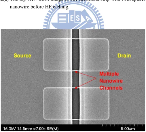
Fig. 2-2(a) The top view SEM image of one sacrificial strip with twin spacer
nanowire before HF etching. ……….40
Fig. 2-2(b) The top view SEM image of one sacrificial strip with twin spacer
nanowire after HF etching. ………....40
Fig. 2-2(c) The corresponding process step of one sacrificial strip with twin spacer nanowire before HF etching in top view. ………..41
Fig. 2-2(d) The corresponding process step of one sacrificial strip with twin spacer nanowire after HF etching in top view. ……….41
Fig. 2-3(a) The tiled view SEM image of multiple nanowire channels after HF
etching. ………..42
Fig. 2-3(b) The corresponding process step of multiple nanowire channels after HF etching in tiled view. ……….42
Fig. 2-4(a) The cross-section SEM image of suspending channels. ………...43
Fig. 2-4(b) The corresponding process flow of multiple nanowire channels after HF etching in cross-section view. ………...43
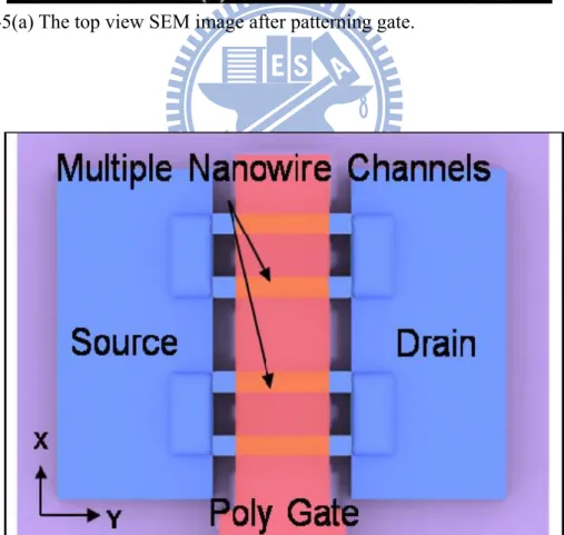
Fig. 2-5(a) The top view SEM image after patterning gate...………...44
Fig. 2-5(b) The corresponding process step after patterning gate in top view..……...44
Fig. 2-6 The cross-section TEM image after patterning gate. ……….45
Fig. 2-7 Transfer characteristics of the CP and the proposed FEN POST SONOS devices………45
Fig. 2-8(a) Transfer characteristics of the CP SONOS device after DC stress at VGS =
Fig. 2-8(b) Transfer characteristics of the FEN POST SONOS device after DC stress at VGS = 7 V condition. ………..46
Fig. 2-9 Transfer characteristics of the CP SONOS device with various programming times at VGS = 15 V………....47
Fig. 2-10 Transfer characteristics of the FEN POST SONOS device with the various programming times at VGS = 15 V………...47
Fig. 2-11 Transfer characteristics of the CP SONOS device with the various erasing times at VGS = -15 V……….48
Fig. 2-12 Transfer characteristics of the FEN POST SONOS device with the various erasing times at VGS = -15 V………48
Fig. 2-13(a) Vth shifts after programming for the CP SONOS and FEN POST SONOS
devices with various gate voltage ………...49
Fig. 2-13(b) Vth shifts after erasing operation for the CP SONOS and FEN POST
SONOS devices with various gate voltage………..49
Fig. 2-14 The distribution of electrical field across the stacked ONO dielectrics for the CP and FEN POST SONOS devices at VGS = 15 V……….…50
Fig. 2-15 The band diagrams of the CP and FEN POST SONOS devices at VGS =
15 V………..50
Fig. 2-16 Retention characteristic of the FEN POST SONOS device after 104 P/E cycles………51
Fig. 2-17 Endurance characteristic of the FEN POST SONOS device. ………..51
Chapter 3
Fig.3-1 The cross-section schematic image after patterning the in-situ doped poly-Si gate. ……….52
Fig. 3-3 The cross-section schematic image after tunneling oxide etched with 1:10 diluted BOE………...……….53
Fig. 3-4 The cross-section schematic image after patterning Al metal pads…………53
Fig. 3-5 The tiled-view SEM image of the FEN POST SONVAS device…………...54
Fig. 3-6 The cross-section schematic image of nanowire channel with vacuum tunneling layer………54
Fig. 3-7 Transfer characteristics of the FEN POST SONVAS device with various programming times at VGS = 15 V……….55
Fig. 3-8 Transfer characteristics of the FEN POST SONVAS device with various erasing times at VGS = 15 V………...55
Fig. 3-9 The distribution of electrical field across the stacked ONO dielectrics for the FEN POST SONOS devices at VGS = 15 V………...56
Fig. 3-10 The distribution of electrical field across the stacked ONO dielectrics for the FEN POST SONVAS devices at VGS = 15 V………...………56
Fig. 3-11 The band diagrams of the FEN POST SONVAS devices at VGS = 15 V.….57
Fig. 3-12 Retention characteristic of FEN POST SONVAS device after 104 P/E cycles………...57
Fig. 3-13 Endurance characteristic of the FEN POST SONOS device………58
Fig. 3-14 The subthreshold swing of the FEN POST SONOS and FEN POST
Chapter 1
Introduction
1-1. Introduction of the Polycrystalline Silicon
Thin-Film Transistor
Polycrystalline silicon (poly-Si) thin film transistors (TFTs) have attracted much attention because of their applications in active matrix displays, such as active matrix liquid crystal displays (AMLCDs) [1] and active matrix organic light emitting displays (AMOLCDs) [2], and potential for the application on three- dimension integrated circuits (3-D ICs). In recent years, the high performances of poly-Si TFTs also have been demonstrated by scaling down device dimensions or utilizing novel crystallization technologies to enhance poly-Si film quality [3, 4]. This provides opportunity of using poly-Si TFTs in integrated peripheral driving circuits.
The possibility of integrating driving circuitry as well as switching devices on
the same substrate represents a major advantage of the polysilicon technology over the amorphous silicon, because the mobility of poly-Si TFTs is usually large than 10 cm2/V-s, that is higher than amorphous Si TFTs and enough for peripheral driving
circuits with n- and p-channel devices. So, the pixel array and the peripheral circuits can be made on the same glass substrate [5-7], a potential system-on-panel (SOP) technology. In addition, due to higher mobility, the poly-Si TFTs can be made smaller compared to that of the amorphous Si TFTs.
In CMOS technology, many high-performance multiple gates structures in a
[10] and gate-all-around [11], have been reported to exhibit superior gate control over the channel than a conventional single-gate MOSFET and reduced short-channel effects.
1-2. Introduction of the SONOS Nonvolatile
Memory Devices
1-2-1. The SONOS Nonvolatile Memory Devices
It is well known that the nonvolatile memory is widely utilized for data storage in portable electronic systems due to its properties of low power consumption and nonvolatility. The conventional floating gate (FG) memory (shown in Fig. 1-1) employed poly-Si film as a charge-storage layer that can achieve high-density integration and good program/erase (P/E) speed; however, there are some concerns regarding the capability to scale down the tunneling dielectric thickness [12]. When the tunneling oxide thickness is below 10 nm, the storage charges in the floating gate lose easily through defects created in the tunneling oxide after repeated P/E cycles [13]. The poly-Si–oxide–nitride–oxide–silicon (SONOS)-type structure memories (shown in Fig. 1-2)have been investigated as an approach to solve the issue of scaling FG memory [14].Due to their spatially isolated deep-level traps, SONOS memories exhibit better charge retention than FG memories that have a bitcell tunneling oxide thickness less than 10 nm. Consequently, a single defect in the tunneling oxide will not lead to the discharge of the memory cell. However, many concerning issues are still presented for SONOS memories. For SONOS memories, erase saturation and
vertical stored charge migration [15, 16] are the major drawbacks. In addition, it is very difficult to promote the P/E speed and data retention simultaneously. In recent years, different device structures [17, 18] and alternating materials [19-21] have been explored to improve the P/E speed and data retention at the same time.
1-2-2. Program/Erase Mechanisms of SONOS Nonvolatile
Memory
In general, the program/erase mechanisms employed in SONOS include channel hot electron injection (CHEI), Fowler-Nordheim tunneling (FN tunneling) and band to band tunneling (BTBT). The three mechanisms will be illustrated in the following sections.
Channel Hot Electron Injection
The channel hot electron injection can be well described by “lucky-electron model” [22]. The injection of channel hot electrons into the gate oxide region occurs at large drain-to-source voltage, as shown schematically in Fig. 1-3. Electrons which flow from source to drain gain energy from the high-field region near the drain junction. Because the effective mass of hole is heavier than the electron, in addition, and the barrier height of valence band is also higher than the conduction band, it is much more difficult for holes to obtain enough energy to surmount the oxide barrier. Therefore, hot-hole injection is rarely employed in nonvolatile memory operation. A merit of CHEI mechanism is to achieve NROM [23], SONOS with 2Bit/Cell. By employing CHEI, the charge can be programmed into drain or source terminals
respectively, then the data can be sensed by “reverse read”.
Fowler-Nordheim Tunneling
The tunneling mechanism is a kind of quantum-mechanical process during which the carriers may tunnel through the forbidden region of the insulator into the allowed states of the insulator or the opposite electrode material. Due to different electric field strength across the insulator, the tunneling mechanism can be classified into direct tunneling and FN tunneling. If the electric field strength across the tunneling oxide
(Eox) is smaller than 1
ox
q t
φ
, where qφ1is the barrier height between Si channel and tunneling oxide, the carriers may tunnel into nitride trapping layer by direct tunneling. The current density is expressed as:
3 2 1 1 1 2 1 2 1 1 ox ox V B E ox ox ox J AE e V V φ φ φ ⎡ ⎤ ⎛ ⎞ ⎢ ⎥ − ⎢− −⎜ ⎟ ⎥ ⎝ ⎠ ⎢ ⎥ ⎣ ⎦ ⎛ ⎞⎛ ⎞ = ⎜ ⎟⎜ − ⎟ ⎝ ⎠⎝ ⎠ ...………(1-1) where 3 2 1 8 q E A h π φ = , 3 2 1 8 2 3 ox m B hq π φ
= , and the electron effective mass, mox, is 0.5m0.
Direct tunneling is illustrated in Fig. 1-4(a). If Eox > 1
ox
q t
φ
, the carriers may tunnel into nitride trapping layer by FN tunneling. The current density is expressed as:
2 ox
B E ox
J = AE e− ....………(1-2)
Band to Band Tunneling
In N-channel devices, when a negative gate voltage and a positive drain voltage are applied to the cell, electron-hole pairs are generated by BTBT in the n+ drain region [1.25]. The phenomenon of BTBT occurs in the n+ drain region overlapping the gate. The strength of electric field in the region must be sufficiently high to cause deep-depletion situation. During the operation, electrons tunnel directly or are assisted by traps in the gap from valence band to conduction band at the drain region. At the same time, holes are generated in the deep-depletion region, and are then accelerated by the strong field and may be attracted by the negative gate bias into the nitride trapping layer. The injection of such hot holes into nitride through the tunnel oxide is used for a new erase operation in N-channel devices [26]. The processes are illustrated in Fig. 1-5.
1-2-3. Reliability of SONOS Nonvolatile Memory
Retention
Retention is a measure of the time that a nonvolatile memory cell can retain the charge in the trapping layer. In nonvolatile memory technology, it is essential to retain data for over ten years. This means the loss of charge stored in the storage medium must be as minimal as possible. Figure 1-6 shows the band diagram for illustrating the charge loss paths in SONOS cells. There are two major leakage current components in relating to charge loss, one is the thermionic emission following Frenkel-Poole mechanism, another one is tunneling through tunneling oxide. The tunneling
mechanisms include trap-to-band (T-B) tunneling, trap-to-trap (T-T) tunneling, and band-to-trap (B-T) tunneling. The trapped electrons in nitride can tunnel back to the conduction band of the silicon substrate (T-B tunneling), or to the interface traps between tunneling oxide and channel (T-T tunneling). In addition, holes from the silicon valence band may tunnel into the nitride traps under the influence of the internal electric field (B-T tunneling).
Endurance
Endurance is the ability of a nonvolatile memory to endure the damage of numerous cycles of programming and erasing, i.e., the number of erase/write cycles that the memory will retain the required memory window and continue to operate as specified in the initial data window. Since the carriers for programming and erasing have energy, they will cause the degradation of tunneling oxide and trapping layer in every operation. In addition, high electric field stress across tunneling oxide will increase the current density at low electric field. The excess current at low electric field after stress is called stress-induced leakage current (SILC) [27]. SILC is attributed to stress-induced oxide defects, which lead to a trap assisted tunneling.
1-3. Motivation
Recently, the high performance poly-Si TFTs were demonstrated to be integrated with peripheral driving circuits [28]. For further achieving system-on-panel (SOP) applications, other functional elements based on poly-Si TFT technology, such as
memories, sensors, drivers, and controllers, are also needed to develop to fully integrate on the same display panel [29-31]. It is well-known that the nonvolatile memory (NVM) is a critical element for data storage, signal processing, and power saving in portable electronic systems [32]. Furthermore, due to the process compatibility, poly-Si TFT silicon–oxide–nitride–oxide–silicon (TFT SONOS) devices, instead of floating-gate type ones, have been considered as a promising candidate NVM for the realization of SOP electronics. However, unlike floating-gate type NVM, conventional planar TFT SONOS (CP SONOS) memories do not have gate-coupling design, thus suffering from the insufficient programming/erasing (P/E) efficiency. To improve this issue, poly-Si protrusion tips, produced by sequential lateral solidified (SLS) crystallization, and nanowire TFT SONOS with a tri-gate structure produced by e-beam lithography have been reported to enhance the electric field to improve the P/E efficiency [33, 34]. However, for SLS method, the location and height of the protrusion tips may be difficult to control. The uniformity of devices may be serious issue. For nanowire by e-beam lithography method, the e-beam lithography is a expensive and slow process, so the cost and throughput are also issues. In this thesis, a field-enhanced nanowire poly-Si TFT SONOS (FEN POST SONOS) with a gate-all-around (GAA) structure and a field-enhanced nanowire poly-Si TFT silicon-oxide-nitride-vacuum-silicon (FEN POST SONVAS) with a gate-all-around (GAA) structure are proposed with a simple process sequence to improve the P/E efficiency and reliability. Using the sidewall spacer method, etch nanowire channel has three sharp corners and the uniformity issue can be suppressed because the size of nanowire channel can be controlled easily by adjusting the relative ion etch (RIE) time. With a GAA structure, the FEN POST SONOS device also has better transistor performance than CP SONOS device due to better gate control ability. So it is a promising candidate for future high density circuits and SOP applications.
1-4. Thesis Organization
In chapter 1, brief introductions of poly silicon TFTs and SONOS nonvolatile memory (NVM) are given to explain the significance and potential of poly silicon TFTs and SONOS nonvolatile memory for future system on panel applications. Then, basic mechanisms of SONOS NVM are illustrated and the motivations of this work are subsequently explained to introduce this thesis.
In chapter 2, the fabrication sequences of FEN POST SONOS memory with a gate-all-around structure are illustrated. The important processes are analyzed by scanning electron microscope (SEM) and transmission electron microscope (TEM). And, the electrical characteristics of FEN POST SONOS are investigated.
In chapter 3, the fabrication sequences of FEN POST SONVAS memory with a gate-all-around structure are illustrated. The important processes are analyzed by scanning electron microscope (SEM). And, the electrical characteristics of FEN POST SONAS are investigated.
Chapter 2
Field-Enhanced-Nanowire Poly-Si TFT
SONOS (FEN POST SONOS) Memory with
a Gate-All-Around Structure
2-1. Introduction
In recent years, poly-Si thin film transistors (TFTs) have been widely used as pixel switching elements in active-matrix displays. For further achieving system-on-panel (SOP) applications, other functional elements based on poly-Si TFT technology, such as memories, sensors, drivers, and controllers, are also required to fully integrate on the same display panel [35-39]. It is well-known that the nonvolatile memory (NVM) is a critical element for data storage, signal processing, and power saving in portable electronic systems [40]. Silicon–oxide–nitride–oxide–silicon (SONOS) flash memory has been investigated to realize vertical scaling of flash memory. The faster programming speed and lower operating voltage of SONOS devices were accomplished in the past by reducing the tunnel-oxide thickness [41-44]. However, this seriously degrades the retention capability of the memory devices. Several efforts have been made to improve the retention time of SONOS devices.And, due to the process is compatible with poly-Si TFT, silicon–oxide–nitride–oxide–silicon (SONOS)-type devices, instead of traditional floating-gate ones, have been considered as a promising nonvolatile memory candidate for future System on Panel (SOP) applications [45-47].
2-2. Fabrication Sequences of FEN POST SONOS
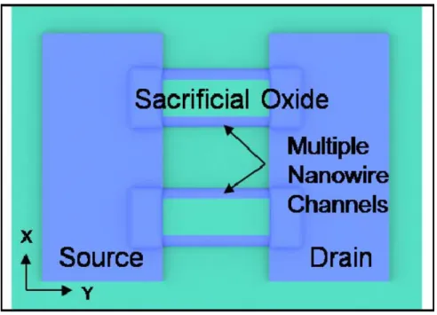
Memory with a Gate-All-Around Structure
The fabrication steps of field-enhanced-nanowire poly-Si TFT SONOS (FEN POST SONOS) with gate-all-around (GAA) structure devices are schematically shown in Fig. 2-1. At first, a 50-nm-thick Si3N4 (as etch-stop layer) and a
300-nm-thick tetra-ethyl-ortho-silicate (TEOS) SiO2 (as sacrificial layer) films were
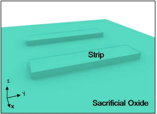
sequentially deposited on oxidized silicon wafer by low pressure chemical vapor deposition (LPCVD) system at 580 °C and 700 °C, respectively. Several strips with step height of 100-nm as shown in Figs. 2-1(a) and 2-1(b) were patterned on surface of the sacrificial SiO2 layer by reactive ion etch (RIE), and followed by a conformal
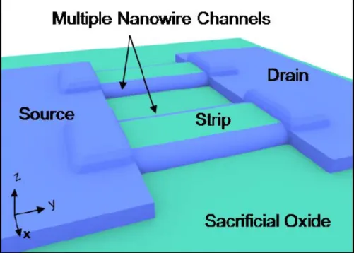
deposition of 100-nm-thick a-Si layer by LPCVD at 550 ℃. After source/drain (S/D)-pad lithography and its RIE process, couples of spacer nanowires were in-situ resided against the sidewall of those designed strips and naturally connected to the S/D pads as shown in Figs. 2-1(c) and 2-1(d), which were formed to be the device active region. It should be noted that each spacer nanowire inherently features three sharp corners, and the nano-scale dimension of the nanowire channels can be defined only by controlling the RIE time without any advanced lithography [48-50], each dummy strip produces twin nanowire channels, as well as the multiple channels can be designed with patterning several dummy strips (n strips x 2 wires/strip = 2n wires). Subsequently, a solid phase crystallization (SPC) at 600 °C in N2 ambient for 24
hours was performed to transform the a-Si into poly-Si. After that, the suspending channels were formed by etching the sacrificial SiO2 layer with 3:50 diluted HF, and
the etching-stopper layer would stop etching process down to the buried oxide as shown in Figs. 2-1(e) and 2-1(f) in the tilted and cross-section views, respectively. Then,
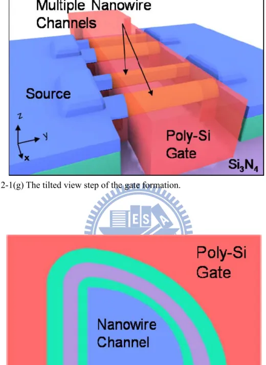
a 5-nm-thick tunneling oxide, a 10-nm-thick nitride trap layer, a 10-nm-thick blocking oxide, and a 200-nm-thick phosphorous in-situ doped poly-Si were sequentially deposited conformally to wrap around those suspending spacer nanowires by LPCVD systems. The poly gate was defined as shown in Figs. 2-1(g) and 2-1(h) in the tilted and cross-section views, respectively, and a phosphorous ion implantation was performed with a dosage of 5×1015cm-2and a energy of 30 keV. Then, a 300-nm-thick passivation oxide deposition and S/D activation were sequentially performed. The contact holes were patterned to etch the passivation layer by RIE and the Al metal layer was deposited by sputter system.Finally, the Al metal layer were patterned and etched by RIE to complete the fabrication. For the purpose of comparison, the conventional planar TFT SONOS (CP SONOS) with single top-gate structure were also fabricated at the same process run.
2-3. Materials Analysis of FEN POST SONOS
Memory with a Gate-All-Around Structure
The previous section briefly describes the process sequence of the FEN POST SONOS. In this section, the scanning electron microscope (SEM) and transmission electron microscope (TEM) have been used to analyze the detailed process parameter in the fabrication of FEN POST SONOS.
Figures 2-2(a) and 2-2(b) show the SEM images before and after sacrificial oxide stripping by HF acid, respectively. And, Figs. 2-2(c) and 2-2(d) show their corresponding schematic images. It can be shown that the sacrificial SiO2layer has
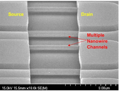
Figures 2-3(a) and 2-3(b) show the tiled-view SEM image and the corresponding schematic image of the multiple suspending nanowire channels after HF etching. Different channel width can be easily designed by adjusting the number of sacrificial SiO2 strips. The cross-section view SEM image and the corresponding schematic
image of the suspending channels are shown in Figs. 2-4(a) and 2-4(b), respectively. The multiple nanowire channels are hung in the air with a height 200 nm above the Si3N4 etch-stop layer and connected to the source and drain pads.With the aid of the
suspending nanowire channels, the ONO dielectric layers and poly gate deposited by LPCVD can be easily surrounding the channel to form the GAA structure. Figures 2-5(a) and 2-5(b) show the top view SEM image and the corresponding schematic image after patterning gate, respectively. It should be noted that there are residual
bottom gates remained below the source/drain extensions after gate patterning. The source/drain extensions shield (prevent) the residual bottom gates from the anisotropic RIE. Figure 2-6 exhibits the cross-section TEM image of each gate-all-around nanowire and shows the ONO dielectrics and poly gate which were conformally deposited on the three sharp corners. The polycrystalline nanowire channel in the center of graph is formed by the TCP-RIE and the dimension of nanowire is precisely controlled by etching time. The TEM image shows that the vertical sidewall thickness, the horizontal width and bevel length of each NW channel are about 85 nm, 85 nm and 130 nm, respectively. Thus the total surrounding width of each NW channel is 300 nm.
2-4. Results and Discussions
The constant drain current method is used to determinate the threshold voltage. The threshold voltage (Vth) is defined as the gate voltage required to achieve a normalized
drain current as 10nA at Vds= 0.1 V
@ 10 th gs ds W V V I nA L = = × ………..(2-1)
where the W and L are the channel width and length, respectively. It should be noted that the channel width of FEN POST SONOS is defined as 0.6n μm (W = n strips × 2 wires/strip × 300 nm/wire = 0.6n μm), where the n is the number of dummy strip. The surrounding width of each nanowire channel is 300 nm as shown in Fig. 2-6. The subthreshold swing (SS) is determined from the subthreshold region of Ids-Vgs curve
at Vds= 0.1 V.
( )
1 log min ds @ 0.1 ds gs I SS V V V − ⎛∂ ⎞ = ⎜⎜ ⎟⎟ = ∂ ⎝ ⎠ …….(2-2)Figure 2-7 shows the transfer characteristics of the CP and the proposed FEN POST SONOS. It is obvious that (as shown in Table 2-1) the FEN POST SONOS with GAA structure device has superior performance than CP device with higher on current, smaller Vth and steeper subthreshold swing (SS), higher on/off ratio, and
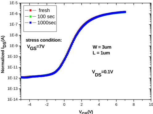
higher mobility, which are contributed to the enhanced gate control ability by the three sharp corners and GAA structure together with the reduced number of grain-boundary defect in the nanowire channel [48]. For memory operations, in this work, the TFT SONOS memory is programmed and erased by Fowler-Nordheim (FN) tunneling mechanism. Figure 2-8(a) and 2-8(b) show the transfer characteristics of the CP and the proposed FEN POST SONOS devices after DC stress at Vgs= 7 V
the stress time is 1000 sec. Thus, the read disturb can be neglected under the normal transistor operation. Figure 2-9 and 2-10 show the transfer characteristics of the CP and FEN POST SONOS devices with various programming times at a gate voltage 15 V, respectively. For erasing operations, the transfer characteristics of the CP and FEN POST SONOS devices with various erasing times at gate voltage -15 V are shown in Figs. 2-11 and 2-12, respectively. It is obviously found that the program/erase (P/E) efficiency of the FEN POST SONOS device is significantly better than the CP one. In the programming characteristics, the FEN POST SONOS exhibit a large Vth shift of 2.71 V in 1 ms at a gate pulse of +15 V, while there is only 0.49 V shift in CP device. The erase characteristics also show that the FEN POST SONOS devices are much faster (a Vth shift of 2.11 V in 1 ms at a gate pulse of -15 V) than the CP counterparts. The improvement on P/E speed and window can be attributed to the field enhancement from the three sharp corners to promote carrier injection through the tunneling oxide into the nitride storage layer. The Vth shifts after programming and
erasing operation for the CP and FEN POST SONOS devices with various voltage are plotted in Figs. 2-13(a) and 2-13(b).
For further clarifying this P/E efficiency enhancement, the simulations of electrical fields for the CP and FEN POST SONOS structures were performed by ISE-TCAD simulator. The distribution of electrical field and band diagrams across the stacked ONO dielectrics was numerically simulated at a gate bias of 15 V for the CP and FEN POST SONOS devices as shown in Fig. 2-14 and 2-15, respectively. The sharp geometry of these three corners enhances the electric field at the Si/tunneling oxide interface and depresses the electric field in the blocking oxide. The large field at the Si/tunneling oxide interface enhances the carrier-injection probability and thus increases both the P/E speeds of FEN POST SONOS device. In addition, the reduction of the electric field in the blocking oxide prevents charges tunneling from
the nitride to the poly-gate and from the poly-gate to the nitride. The P/E activity is thus facilitated between the channel and tunneling oxide rather than between the blocking oxide and the gate. In contrast, for CP SONOS structures, as shown in Fig. 2-14, the electric field in the tunneling oxide is equal to that in the blocking oxide, leading to lower P/E efficiency. In addition, Figure 2-15 exhibits the FEN POST SONOS device has shorter tunneling distance than the CP SONOS device. Figure 2-16 shows the retention characteristic of FEN POST SONOS device, where the memory window is maintained with negligible degradation up to the tested time of 104 sec. It shows the memory window will be larger than 1.1 V after extrapolating to retention time of 10 years. The endurance characteristic of FEN POST SONOS device is shown in Fig. 2-17, the memory window was kept 1.68V and rises about 1 V after 104 P/E cycles. The rising of memory window results from both the charges in Si3N4
deep level traps are hard to be erased and the subthreshold swing is degradation due to the tunneling oxide is damaged during P/E cycles.
2-5. Summary
In summary, we have demonstrated the FEN POST SONOS devices, the FEN POST SONOS devices have superior performance than CP devices with higher on current, smaller Vth, steeper subthreshold swing (SS), higher on/off ratio, and higher
mobility which are contributed to the enhanced gate control ability by the three sharp corners and GAA structure together with the reduced number of grain-boundary defect in the nanowire channel. In addition, the proposed FEN POST SONOS exhibits higher P/E speed than CP SONOS due to larger electric field in the tunneling layer
and lower electric field in the blocking oxide. The proposed FEN POST SONOS also exhibits stable endurance/retention characteristics. And, the process simplicity and good device performance is very promising for future SOP and 3-D ICs applications.
Chapter 3
Field-Enhanced-Nanowire Poly-Si TFT
Silicon-Oxide-Nitride-Vacuum-Silicon
(FEN POST SONVAS) Memory With a
Gate-All-Around Structure
3-1. Introduction
The conventional SONOS-type memories use SiO2 as blocking oxide and tunnel
dielectric, which may be modified to achieve higher speed and lower voltage operation by using high-k dielectric as blocking oxide [51-53]. Less voltage dropped in blocking layer and more voltage dropped in tunneling layer when using high-k dielectric for blocking dielectric, so the program/erase efficiency can be enhanced. In addition, the use of high-k material as the tunnel dielectric and trapping layer has also been introduced to enable further scaling [54-57].
Endurance is the ability of a nonvolatile memory to endure the damage of numerous cycles of programming and erasing, i.e., the number of program/erase cycles that the memory will retain the required memory window.Since the carriers for programming and erasing have energy, they will cause the degradation of tunneling oxide and trapping layer in every operation. In previous chapter, Fig. 2-16 shows the endurance characteristic of FEN POST SONOS. The memory window rising results from both the charges in Si3N4 deep level traps are hard to be erased and the
subthreshold swing is degradation due to the tunneling oxide is damaged during P/E cycles. To suppress the degradation of tunneling oxide during P/E cycles, we
proposed a field-enhanced-nanowire poly-Si TFT silicon-oxide-nitride-vacuum-silicon (FEN POST SONVAS) structure which
tunneling oxide was replaced with vacuum. So, the damage of tunneling layer during P/E operation can be suppressed. In other words, the FEN POST SONVAS structure can enhance the endurance characteristic of the devices. In addition, in this work, we used the low-k (vacuum) material to replace the tunneling oxide to enhance the endurance characteristics. At the same time, the lowest-k property of vacuum make higher voltage dropped in the vacuum tunneling layer. This phenomenon can enhance the electric filed in tunneling and lower the electric field in blocking oxide. In other words, the program/erase efficiency can be enhanced similar as the introduction of high-k blocking dielectric.
3-2. Fabrication Sequences of FEN POST SONVAS
with a Gate-All-Around Structure
The fabrication sequence of proposed FEN POST SONOS memory has been described in the previous chapter. A 5-nm-thick tunneling oxide, a 10-nm-thick nitride trap layer, a 10-nm-thick blocking oxide, and a 200-nm-thick phosphorous
in-situ doped poly-Si were sequentially deposited conformally to wrap around those suspending spacer nanowires by LPCVD systems after sacrificial oxide was removed by diluted HF. After gate patterning, the in-situ doped poly-Si, blocking oxide and Si3N4 trap layer were etched out by RIE and tunneling oxide was still remained as
shown in cross-section schematic image in Fig. 3-1. A phosphorous ion implantation was performed with a dosage of 5×1015cm-2and an energy of 35 keV. A 200-nm-thick
Si3N4 was deposited and then etched back to form two Si3N4 spacers resided against
the poly-Si gate and on the tunneling oxide layer as shown in cross-section schematic image in Fig. 3-2. The tunneling oxide was side-etched for 350-nm with (1:10) diluted BOE as shown in Fig. 3-3. A 300-nm-thick passivation oxide was deposited by SiH4-based PECVD system and the remaining processes were same as the previous
FEN POST SONOS device. The FEN POST SONVAS structure is shown in cross-section schematic image in Fig. 3-4.
3-3. Materials Analysis of FEN POST SONVAS with
a Gate-All-Around Structure
The previous section briefly describes the process sequence of the FEN POST SONVAS device. In this section, the scanning electron microscope (SEM) and transmission electron microscope (TEM) have been used to analyze the detailed process parameter in the fabrication of FEN POST SONVAS.
Figure 3-5 exhibits the tiled-view SEM image of the FEN POST SONVAS device. It shows the nitride spacers resided against the S/D extensions and the empty gap on the nanowire channel. The cross-section schematic image of nanowire channel with vacuum tunneling layer as shown in Fig. 3-6.
3-4. Results and Discussions
by Fowler-Nordheim (FN) tunneling mechanism. Figure 3-7 show the transfer characteristics of the FEN POST SONVAS devices with various programming times at a gate voltage of 15 V. For erasing operations, the transfer characteristics of the FEN POST SONVAS devices with various erasing times at gate voltage of -15 V are shown in Figs. 3-8. The Vth shifts after programming and erasing operation at a gate
voltage 15 V and -15 V, respectively, for the CP, FEN POST SONOS and FEN POST SONVAS devices are shown in Table 3-1. It is clear found that the program/erase (P/E) efficiency of the FEN POST SONVAS device is better than the FEN POST SONOS.
For further clarifying this P/E efficiency enhancement, the simulations of electrical field for the FEN POST SONOS and FEN POST SONVAS structures were performed by ISE-TCAD simulator. The distribution of electrical field across the stacked ONO dielectrics was numerically simulated at a gate bias of 15 V for the FEN POST SONOS and FEN POST SONVAS devices as shown in Figs. 3-9 and 3-10, respectively. Figs. 3-9 and 3-10 indicate that the FEN POST SONVAS device has larger electric field in the tunneling layer and lower electric field in the blocking oxide. The larger electric field in the vacuum layer results from its low-k property. There is higher percentage of voltage dropped in the vacuum layer. The large field in the vacuum layer enhances the carrier-injection probability and thus increases both the P/E speeds in FEN POST SONVAS device. In addition, the reduction of the electric field in the blocking oxide prevents charges tunneling from the nitride to the poly-gate and from the poly-gate to the nitride. The P/E activity is thus facilitated between the channel and vacuum layer rather than between the blocking oxide and the gate. The band diagram was numerically simulated at a gate bias of 15 V for the FEN POST SONVAS device as shown inFig. 3-11. It shows the FEN POST SONVAS device also has shorter tunneling distance. Fig. 3-12 shows the retention characteristics of FEN
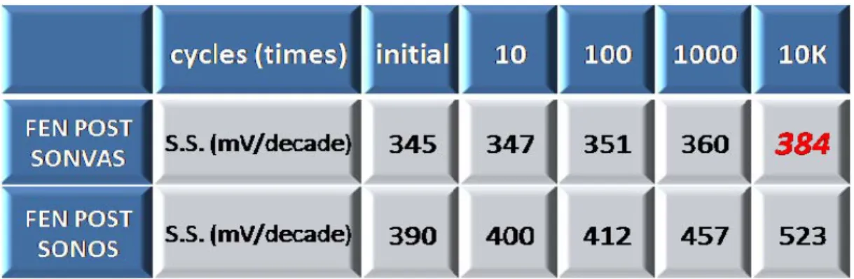
POST SONOS and FEN POST SONVAS devices after 104 cycles, where the memory windowof FEN POST SONVAS device is maintained with little degradation up to the tested time of 104 sec. It shows the memory window will be larger than 1.4 V after extrapolating to retention time of 10 years. The larger memory window after extrapolating to retention time of 10 years for FEN POST SONVAS device results from its higher P/E speed. The endurance characteristic of FEN POST SONVAS device is shown in Fig. 3-13. The 2.4-V memory window was kept and the window rises only 0.5 V after 104 P/E cycles. The less memory window shift after 104 P/E cycles for FEN POST SONVAS device results from less dangling bonds and interface traps produced during P/E cycles. The subthreshold swing of FEN POST SONOS and FEN POST SONVAS devices after P/E cycles is shown in Fig. 3-14 and Table 3-2, respectively. The subthreshold swing of FEN POST SONOS device changed from 390 mV/decade to 523 mV/decade and that of FEN POST SONVAS device changed only from 345 mV/decade to 384 mV/decade after 104 P/E cycles.
3-5. Summary
In summary, we have demonstrated the poly-Si FEN POST SONOS structure in the previous chapter; the proposed FEN POST SONOS device exhibits superior memory device characteristics with higher P/E efficiency and stable endurance/retention characteristics. And, the process simplicity is very promising for future SOP applications. In this chapter, we have demonstrated the FEN POST SONVAS structure. The proposed FEN POST SONVAS device exhibits higher P/E speed than FEN POST SONOS due to larger electric field in the tunneling layer and
lower electric field in the blocking oxide. In addition, the FEN POST SONVAS device also exhibits better data retention and endurance characteristics than the previous FEN POST SONOS device.
Chapter 4
Conclusions
In this thesis, novel FEN POST SONOS and FEN POST SONVAS memory devices with gate-all-around structures have been demonstrated in previous chapters. In this chapter, the both memory devices are discussed and summarized in detail.
In chapter 2, a simple and cost-effective method was performed to fabricate the FEN POST SONOS device. The simple spacer technique was used to form the nanowire channels without any advanced lithography. The FEN POST SONOS devices have superior performance than CP SONOS devices with higher on current, smaller Vth, steeper subthreshold swing (SS), higher on/off ratio, and higher mobility,
which are contributed to the enhanced gate controllability by the three sharp corners and GAA structure together with the reduced number of grain-boundary defect in the nanowire channel. In addition, the proposed FEN POST SONOS device exhibits higher P/E speed due to much enhanced electric field in the tunneling layer and lower electric field in the blocking oxide as compared to the CP SONOS devices. The FEN POST SONOS device exhibited a Vth shift of 2.71 V and 2.11 V at VGS = +15/-15 V
in 1 ms for FN programming and erasing operations, respectively; while the reference CP SONOS devices only showed the negligible change. And, the FEN POST SONOS devices also showed stable retention and reasonable endurance characteristics. For retention, the FEN POST SONOS device maintained 1.1V memory window after ten years. For endurance, the FEN POST SONOS device kept 1.68V memorywindow after 104 P/E cycles.
In chapter 3, a novel FEN POST SONVAS device which tunneling oxide was replaced with vacuum is demonstrated in this work. The proposed FEN POST
SONVAS device exhibits higher P/E speed than FEN POST SONOS device due to larger electric field in the vacuum tunneling layer and lower electric field in the blocking oxide. It exhibited a Vth shift of 3.17V and 2.68 V at VGS = +15/-15 V in 1
ms for programming and erasing operations, respectively. And, the FEN POST SONVAS device also showed better retention and endurance characteristics. For retention, the FEN POST SONVAS maintained 1.4V memory window after ten years. For endurance, the FEN POST SONVAS kept 2.4V memory window and only 0.5V memory window shift.
Since the FEN POST SONOS and FEN POST SONVAS devices exhibited excellent performance, such as good electrical characteristics, high P/E efficiency, and stable reliability, they are very promising for the future applications in SOP and 3-D ICs.
References
[1] A. A. Orouji and M. J. Kumar, “Leakage current reduction techniques in poly-Si TFTs for active matrix liquid crystal displays: a comprehensive study,” IEEE Trans.
Device and Material reliability, vol. 6, no. 2, pp. 315-325, 2006.
[2] M. Stewart, R. S. Howell, L. Pires, and M. K. Hatalis, “Polysilicon TFT technology for active matrix OLED displays,” IEEE Trans. Electron Devices, vol. 48, pp. 845-851, 2001.
[3] H. Kuriyama et al., “An asymmetric memory cell using a C-TFT for ULSI SRAM,” Symp. On VLSI Tech., pp.38-39, Jun.1992
[4] T. Yamanaka, T. Hashimoto, N. Hasegawa, T. Tanala, N. Hashimoto, A. Shimizu, N. Ohki, K. Ishibashi, K. Sasaki, T. Nishida, T. Mine, E. Takeda, and T. Nagano, “Advanced TFT SRAM cell technology using a phase-shift lithography,” IEEE Trans.
Electron Devices, Vol. 42, pp.1305-1313,1995.
[5] K. Nakazawa, “Recrystallization of amorphous silicon films deposited by low-pressure chemical vapor deposition from Si2H6 gas,” J. Appl. Phys, vol. 69,pp.
1703-1706, 1991
[6] T. J. King and K. C. Saraswat, “Low-temperature fabrication of poly-Si thin-film transistors,” IEEE Electron Device Lett., vol. 13, pp. 309-311, 1992.
[7] H. Kuriyama, S. Kiyama, S. Noguchi, T. Kuahara, S. Ishida, T. Nohda, K. Sano, H. Iwata, S. Tsuda, and S. Nakano, “High mobility poly-Si TFT by a new excimer laser annealing method for large area electronics,” IEDM Tech. Dig, vol. 91, pp. 563-566, 1991.
[8] K. Suzuki, T. Tanaka, Y. Tosaka, H. Horie, and Y. Arimoto, “Scaling theory for double-gate SOI MOSFET's,” IEEE Trans. Electron Devices, vol. 40, pp. 2326-2329,
Dec. 1993.
[9] B. S. Doyle, S. Datta, M. Doczy, S. Hareland, B. Jin, J. Kavalieros, T. Linton, A. Murthy, R. Rios and R. Chau., “High Performance Fully-Depleted Tri-Gate CMOS Transistors ,”IEEE Trans. Electron Device Lett., vol. 24, pp. 263-265, Apr., 2003. [10] N.Lindert, L Chang, Y. K. Choi, E. H. Anderson, W. C. Lee, T. J. King, J. Bokor, and C. Hu., “Sub-60-nm Quasi-Planar FinFETs Fabricated Using a Simplified Process,” IEEE Trans. Electron Device Lett., vol. 22, pp. 487-489, Oct., 2001.
[11] S. Miyamoto, S. Maegawa, S. Maeda, T. Ipposhi, H. Kuriyama, T. Nishimura, and N. Tsubouchi, “Effect of LDD structure and channel poly-Si thinning on a gate-all-around TFT (GAT) for SRAM's,” IEEE Trans. Electron Devices, vol. 46, pp. 1693-1698, Aug. 1999.
[12] J. J. Lee, X. Wang, W. Bai, N. Lu, and D. L. Kwong, “Theoretical and experimental investigation of Si nanocrystal memory device with HfO2 high-k
tunneling dielectric,” IEEE Trans. Electron Devices, vol. 50, no. 10, pp. 2067–2072, Oct. 2003.
[13]B. D. Salvo, C. Gerardi, R. V. Schaijk, S. A. Lombardo, D. Corso, C. Plantamura, T. Serafino, G. Ammendola, M. V. Duuren, P. Goarin, W. Y. Mei, K. V. D. Jeugd, H. Baron, M. Gely, P. Mur, and S. Deleonibus, “Performance and reliability features of advanced nonvolatile memories based on discrete traps (silicon nanocrystals, SONOS),” IEEE Trans. Device Mater. Rel., vol. 4, no. 3, pp. 377–389, Sep. 2004. [14] J. H. Kim and J. B. Choi, “Long-term electron leakage mechanisms through ONO interpoly dielectric in stacked-gate EEPROM cells,” IEEE Trans. Electron
Devices, vol. 51, no. 12, pp. 2048–2053, Dec. 2004.
[15] P. Xuan, M. She, B. Harteneck, A. Liddle, J. Bokor, and T. J. King, “FinFET SONOS flash memory for embedded applications,” IEDM Tech. Dig., 2003, pp. 609–613.
[16] T. Sugizaki, M. Kobayashi, M. Ishidao, H. Minakata, M. Yamaguchi, Y. Tamura, Y. Sugiyama, T. Nakanishi, and H. Tanaka, “Novel multi-bit SONOS type flash memory using a high-k charge trapping layer,” in VLSI Symp. Tech. Dig., pp. 27–28, 2003.
[17] T. S. Chen, K. H. Wu, H. Chung, and C. H. Kao, “Performance improvement of SONOS memory by bandgap engineer of charge trapping layer,” IEEE Electron
Device Lett., vol. 25, no. 4, pp. 205–207, Apr. 2002.
[18] R. Ohba, Y. Mitani, N. Sugiyama, and S. Fujita, “25 nm planar bulk SONOS-type memory with double tunnel junction,” in IEDM Tech. Dig., pp. 37.1.1–37.1.4, 2006.
[19] H. C. You, T. H. Hsu, F. H. Ko, J. W. Huang, W. L. Yang, and T. F. Lei, “SONOS-type flash memory using an HfO2 as a charge trapping layer deposited by
the sol–gel spin-coating method,” IEEE Electron Device Lett., vol. 27, no. 8, pp. 653–655, Aug. 2006.
[20] T. H. Hsu, H. C. You, F. H. Ko, and T. F. Lei, “PolySi–SiO2–ZrO2– SiO2–Si
flash memory incorporating a sol–gel-derived ZrO2 charge trapping layer,” J.
Electrochem. Soc., vol. 153, no. 11, pp. 934–937, Nov. 2006.
[21] Y. Q. Wang, D. Y. Gao, W. S. Hwang, C. Shen, G. Zhang, G. Samudra, Y. C. Yeo, and W. J. Yoo, “Fast erasing and highly reliable MONOS type memory with HfO2 high-k trapping layer and Si3N4/SiO2 tunneling stack,” in IEDM Tech. Dig., pp.
37.4.1–37.4.4, 2006.
[22] C. Hu, “Lucky-electron model of channel hot electron emission”, IEDM, vol. 25, pp.22-25, 1979.
[23] B Eitan, P Pavan, I. Bloom, E. Aloni, A. Frommer, D. Finzi, “Can NROM, a 2-bit trapping storage cell, give a real challenge to floating gate cells?”, SSDM, 1999. [24] J. Moll, Physics of Semiconductors. New York: McGraw-Hill, 1964.
[25] M. Lezlinger and E. H. Snow, J. Appl. Phys., 40, 278 ,1969.
[26] San, K.T.; Kaya, C.; Ma, T.P.; “Effects of erase source bias on flash EPROM device reliability” Electron Devices, IEEE Transactions, vol 42, no. 1, pp. 150-159, Jan. 1995.
[27] K. Naruke, S. Taguchi, and M. Wada, “Stress Induced Leakage Current Limiting to Scale Down EEPROM Tunnel Oxide Thickness”, IEDM Tech. Dig., pp. 424-427, 1988.
[28] T. Aoyama, K. Ogawa,Y. Mochizuki, and N.Konishi, “Inverse staggered poly-Si and amorphous Si double structure TFT's for LCD panels with peripheral driver circuits integration,” IEEE Trans. Elec. Dev., no. 43, pp. 701-705, 1996
[29] K. Yoneda, R. Yokoyama, and T. Yamada, “Development trends of LTPS TFT LCDs for mobile applications,” in VLSI Symp. Circuit. Dig., pp. 85–90, 2001.
[30] T.Nishibe andH.Nakamura, “Value-added circuit and function integration for SOG (system-on glass) based on LTPS technology,” in Proc. SID, pp. 1091–1094, 2006.
[31] C. S. Tan, W. T. Sun, S. H. Lu, C. H. Kuo, I. T. Chang, S. H. Yeh, C. C. Chen, L. Liu, Y. C. Lin, and C. S. Yang, “A simple architecture for fully integrated poly-Si TFT-LCD,” in Proc. SID, pp. 336–339, 2005.
[32] J.-H. Kim, I. W. Cho, G. J. Bae, and I. S. Park, “Highly manufacturable SONOS non-volatile memory for the embedded SoC solution,” in VLSI Symp. Tech. Dig., pp. 31–32, 2003.
[33] S.-I. Hsieh, H.-T. Chen, Y.-Ch. Chen, Ch.-L. Chen, and Y.-C. King, “MONOS memory in sequential laterally solidified low-temperature poly-Si TFTs,” IEEE
Electron Device Lett., vol. 27, no. 6, pp. 272–274, Jun. 1999.
[34] S.-C. Chen, T.-C. Chang, P.-T. Liu, Y.-C. Wu, P.-S. Lin, B.-H. Tseng, J.-H. Shy, S. M. Sze, C.-Y. Chang, and C.-H. Lien, “A novel nanowire channel poly-Si TFT functioning as transistor and nonvolatile SONOS memory,” IEEE Electron Device
Lett., vol. 28, no. 9, pp. 809–811, Sep. 2007.
[35] K. Yoneda, R. Yokoyama, and T. Yamada, “Development trends of LTPS TFT LCDs for mobile applications,” in VLSI Symp. Circuit. Dig., pp. 85–90, 2001.
[36] T. Nishibe and H. Nakamura, “Value-added circuit and function integration for SOG (system-on glass) based on LTPS technology,” in Proc. SID, pp. 1091–1094, 2006.
[37] C. S. Tan, W. T. Sun, S. H. Lu, C. H. Kuo, I. T. Chang, S. H. Yeh, C. C. Chen, L. Liu, Y. C. Lin, and C. S. Yang, “A simple architecture for fully integrated poly-Si TFT-LCD,” in Proc. SID, pp. 336–339, 2005.
[38] B. Lee, Y. Hirayama, Y. Kubota, S. Imai1, A. Imaya, M. Katayama, K. Kato, A. Ishikawa, T. I. Ikeda, Y. Kurokawa, T. Ozaki, K. Mutaguch, and S. Yamazaki, “A CPU on a glass substrate using CG-silicon TFTs,” in ISSCC Tech. Dig., pp. 164–165, 2003.
[39] N.-I. Lee, J.-W. Lee, H.-S. Kim, and C.-H. Han, “High-performance EEPROM’s using N- and P-channel polysilicon thin-film transistors with electron cyclotron resonance–Plasma oxide,” IEEE Electron Device Lett., vol. 20, no. 1, pp. 15–17, Jan. 1999.
[40] J.-H. Kim, I. W. Cho, G. J. Bae, and I. S. Park, “Highly manufacturable SONOS non-volatile memory for the embedded SoC solution,” in VLSI Symp. Tech. Dig., pp. 31–32, 2003.
[41] M. H. White, Y. Yang, P. Ansha, and M. L. French, “A low voltage SONOS nonvolatile semiconductor memory technology,” IEEE Trans. Compon., Packag.,
Manuf. Technol. A, vol. 20, no. 2, pp. 190–195, Jun. 1997.
[42] M. French, H. Sathianathan, and M. White, “A SONOS nonvolatile memory cell for semiconductor disk application,” in Proc. IEEE Nonvolatile Memory Technol.
[43 ] M. H. White, D. A. Adams, and J. Bu, “On the go with SONOS,” IEEE Circuits
Devices Mag., vol. 16, no. 4, pp. 22–31, Jul. 2000.
[44] S. Mori, Y. Y. Araki, M. Sato, H. Meguro, H. Tsunoda, E. Kamiya, K. Yoshikawa, N. Arai, and E. Sakagami, “Thickness scaling limitation factors of ONO interpoly dielectric for nonvolatile memory devices,” IEEE Trans. Electron Devices, vol. 43, no. 1, pp. 47–53, Jan. 1996.
[45] Y. Nakajima, Y. Kida, M. Murase, Y. Toyoshima, and Y. Maki, “Latest development of ‘System-on-Glass’ display with low temperature poly-Si TFT,” in
Proc. SID, pp. 864–867, 2004.
[46] P.-T. Liu, C. S. Huang, and C. W. Chen, “Nonvolatile low-temperature polycrystalline silicon thin-film-transistor memory devices with oxide-nitride-oxide stacks,” Appl. Phys. Lett., vol. 90, pp. 182115-1-182115-3, 2007.
[47] S.-C. Chen, T.-C. Chang, P.-T. Liu, Y.-C. Wu, P.-S. Lin, B.-H. Tseng, J.-H. Shy, S. M. Sze, C.-Y. Chang, and C.-H. Lien, “A novel nanowire channel poly-Si TFT functioning as transistor and nonvolatile SONOS memory,” IEEE Electron Device
Lett., vol. 28, no. 9, pp. 809–811, Sep. 2007.
[48] T.-C. Liao,S.-W. Tu, M. H. Yu, W.-K. Lin, C.-C. Liu, K.-J. Chang, Y.-H. Tai, and H.-C. Cheng, “Novel gate-all-around poly-Si TFTs with multiple nanowire channels,” IEEE Electron Device Lett., vol. 29, no. 8, pp. 889–891, Aug. 2008.
[49] C.-J. Su, H.-C. Lin, H.-H Tsai, H.-H. Hsu, T.-M. Wang, T.-Y. Huang, and W.- X. Ni, “Operations of poly-Si nanowire thin-film transistors with a multiple-gated configuration,” Nanotechnology, vol. 18, pp. 1–7, 2007.
[50] Y.-K. Choi, T.-J. King, and C. Hu, ”Nanoscale CMOS spacer FinFET for the terabit era,” IEEE Electron Device Lett., vol. 23, no. 1, pp. 25–27, Jan. 2002.
[51] C. H. Lee, K. I. Choi, M. K. Cho, Y. H. Song, K. C. Park, and K. Kim, “A novel SONOS structure of SiO2/SiN/Al2O3 with TaN metal gate for multi-giga bit flash
memories,” in IEDM Tech. Dig., pp. 613–616, 2003.
[52] C.-H. Lee, J. Choi, C. Kang, Y. Shin, J.-S. Lee, J. Sel, J. Sim, S. Jeon, B.-I. Choe, D. Bae, K. Park, and K. Kim, “Multi-level NAND flash memory with 63 nm-node TANOS (Si−Oxide−SiN−Al2O3−TaN) cell structure,” in VLSI Symp. Tech. Dig., pp.
21–22, 2006.
[53] Y. Park, J. Choi, C. Kang, C. Lee, Y. Shin, B. Choi, J. Kim, S. Jeon, J. Sel, J. Park, K. Choi, T. Yoo, J. Sim, and K. Kim, “Highly manufacturable 32-Gb multi-level NAND flash memory with 0.0098 μm2 cell size using TANOS (Si−Oxide−Al2O3−TaN) cell technology,” in IEDM Tech. Dig., pp. 29–32, 2006.
[54] M. She, H. Takeuchi, and T.-J. King, “Silicon-nitride as a tunnel dielectric for improved SONOS-type flash memory,” IEEE Electron Device Lett., vol. 24, no. 5, pp. 309–311, May 2003.
[55] X. Wang, “A novel MONOS-type nonvolatile memory using high-k dielectrics for improved data retention and programming speed,” IEEE Trans. Electron Devices, vol. 51, no. 4, pp. 597–602, Apr. 2004.
[56] Hsin-hao Hsu, Ingram Yin-ku Chang, and Joseph Ya-min Lee, “Metal–Oxide–High-κ Dielectric–Oxide–Semiconductor (MOHOS) Capacitors and Field-Effect Transistors for Memory Applications,” IEEE Electron Device Lett., vol. 28, no. 11, pp. 964–966, Nov. 2007.
[57] Tahui Wang, H. C. Ma, C. H. Li, Y. H. Lin, C. H. Chien, and T. F. Lei, “Charge Retention Loss in a HfO2 Dot Flash Memory via Thermally Assisted Tunneling,”
Table 2-1 Electrical characteristics of the FEN POST SONOS and CP SONOS devices.
Table 3-1 The Vth shifts after programming and erasing operation at VGS= 15 V and
-15 V for the CP, FEN POST SONOS and FEN POST SONVAS devices.
Table 3-2 The subthreshold swing of FEN POST SONOS and FEN POST SONVAS devices after P/E cycles.
Fig. 1-1 The structure of the conventional floating gate nonvolatile memory device. The poly-Si floating gate is used as the charge storage element.
Fig. 1-2 The structure of the SONOS nonvolatile memory device. The nitride layer is used as the charge-trapping element.
Fig. 1-3 Proposed trajectory of an emitted channel electron. An energetic electron is redirected toward the interface by an acoustic phonon scattering.
Fig. 1-4 (a) Direct tunneling is associated with transversal of a trapezoidal barrier. (b) Fowler-Nordheim Tunneling is associated with transversal of a triangular barrier.
Fig. 1-5 Illustration of Band to band tunneling. (a) Electron-hole pair appear in the deep-depletion region layer in the n+ drain. (b) The path of electron-hole pair in energy band diagram.
Fig. 1-6 Band diagram of trapped charges loss path in SONOS: tpap-to-band tunneling (T-B), tpap-to-trap tunneling (T-T), band-to-trap tunneling (B-T), thermal excitation (TE) and Frenkel-Poole emission (PF).
Fig. 2-1(a) The tilted view process step of the strip formation.
Fig. 2-1(c) The tilted view step of the nanowire-channel formation.
Fig. 2-1(e) The tilted view step of the suspending nanowire-channel formation.
Fig. 2-1(f) The cross-section view step of the suspending nanowire-channel formation.
Fig. 2-1(g) The tilted view step of the gate formation.
Fig. 2-2(a) The top view SEM image of one sacrificial strip with twin spacer nanowire before HF etching.
Fig. 2-2(b) The top view SEM image of one sacrificial strip with twin spacer nanowire after HF etching.
Fig. 2-2(c) The corresponding process step of one sacrificial strip with twin spacer nanowire before HF etching in top view.
Fig. 2-2(d) The corresponding process step of one sacrificial strip with twin spacer nanowire after HF etching in top view.
Fig. 2-3(a) The tiled view SEM image of multiple nanowire channels after HF etching.
Fig. 2-3(b) The corresponding process step of multiple nanowire channels after HF etching in tiled view.
Fig.2-4(a) The cross-section SEM image of suspending channels.
Fig. 2-4(b) The corresponding process flow of multiple nanowire channels after HF etching in cross-section view.
Fig. 2-5(a) The top view SEM image after patterning gate.
Fig. 2-6 The cross-section TEM image after patterning gate.
Fig. 2-7 Transfer characteristics of the CP and the proposed FEN POST SONOS devices. -8 -6 -4 -2 0 2 4 6 8 10 1E-14 1E-13 1E-12 1E-11 1E-10 1E-9 1E-8 1E-7 1E-6 1E-5 V DS=0.1V W = 3um (5 pairs Nanowire) L = 1um No rm aliz ed I DS (A) VGS(V) FEN POST SONOS CP SONOS
Fig. 2-8(a) Transfer characteristics of the CP SONOS device after DC stress at VGS =
7 V condition.
Fig. 2-8(b) Transfer characteristics of the FEN POST SONOS device after DC stress at VGS = 7 V condition. -4 -2 0 2 4 6 8 10 1E-14 1E-13 1E-12 1E-11 1E-10 1E-9 1E-8 1E-7 1E-6 1E-5 V DS=0.1V W = 3um L = 1um N o rm al iz ed I DS (A) VGS(V) fresh 100 sec 1000sec stress condition: VGS=7V -4 -2 0 2 4 6 8 10 1E-14 1E-13 1E-12 1E-11 1E-10 1E-9 1E-8 1E-7 1E-6 1E-5 W = 3um (5 pairs Nanowire) L = 1um V DS=0.1V No rmal ize d I DS (A ) VGS(V) fresh 100sec 1000sec stress condition VGS= 7 V