In this study, the Cu(300 nm)–CoSi2(50 nm)/n+p junction diodes were intact with respect to metallurgical reaction up to a 350 C thermal annealing while the electrical characteristics started to degrade after annealing at 300 C in N2 ambient for 30 min. With the addition of a 50-nm-thick TaN diffusion barrier between Cu and CoSi2, the junction diodes were able to sustain annealing up to 600 C without losing the basic integrity of the device characteristics, and no metallurgical reaction could be observed even after a 750 C annealing in furnace. In addition, the structure of TaN layers deposited on CoSi2 at various nitrogen flow rates has been investigated. The TaN film with small grain sizes deposited at nitrogen flow ratios exceeding 10% shows better barrier capability against Cu diffusion than the others.
Index Terms—Cobalt, copper, diffusion barrier, junction, nitrogen, tantalum.
I. INTRODUCTION
F
OR A long time, metal silicides had proven valuable to both ohmic and Schottky contacts. Aside from applications as ohmic or Schottky contacts, high conductivity metal silicides were proposed in 1979 as contacts to doped polysilicon or poly-cide structure to reduce resistance and give extra interconnec-tion capability [1]. In 1981, the concept was extended to diffu-sion areas by forming self-aligned silicide at both polysilicon and diffusion areas simultaneously for improving both contact and interconnects [2]. Silicide-related technologies have there-fore become an integral part of submicron devices in recent years.The current trend in shrinking integrated circuits to improve the performance of chips requires substituting copper (Cu) for aluminum as interconnects in the deep submicron-integrated circuits [3], [4]. Recently, copper has been used as the global interconnect material for ultralarge-scale integration (ULSI)
cir-Manuscript received April 24, 2002. This work was supported in part by the National Science Council, Taiwan, R.O.C., under Contract NSC-90-2215-E-035-007 and the Feng Chia University (FCU-RD-88-01). The review of this paper was arranged by Editor R. Shrivastava.
W. L. Yang is with the Department of Electronic Engineering, Feng Chia University, Taichung, Taiwan, R.O.C. (e-mail: [email protected]).
W.-F. Wu is with National Nano Device Laboratories, Hsinchu, Taiwan, R.O.C.
H. C. You and T. F. Lei are with the Institute and Department of Electronics, National Chiao Tung University, Hsinchu, Taiwan, R.O.C.
K.-L. Ou and C.-P. Chou are with the Institute and Department of Mechanical Engineering, National Chiao Tung University, Hsinchu, Taiwan, R.O.C.
Digital Object Identifier 10.1109/TED.2002.804692
terconnects for high-speed ULSI circuits.
It is well known that Cu forms Cu–Si compounds at very low temperatures (200 C) [6] and also introduces deep level traps in silicon, a phenomenon that deteriorates device performance [7]. Therefore, the realization of thermally stable Cu-contacted sys-tems suppressing mass transport over interface due to the high diffusivity and reactivity of Cu is an essential issue in the use of Cu as a local interconnect material. Since copper is directly in contact with the source–drain area of MOSFETs in the local interconnects, it is expected that direct contact between copper and metal-silicided junction is inevitable. In recent years, CoSi has received a lot of attention due to its superior characteristics, compared to TiSi , on issues of phase transformation, bridging effect, and chemical stability [8]. Unfortunately, Cu was found to diffuse across the silicide layer and form the Cu–Si compound below the silicide layer in the Cu–CoSi –Si systems [9], [10]. Because the reaction in the Cu–silicide–Si structure occurs at a relatively low temperature, an effective diffusion barrier layer is required for the application of the Cu–silicide–Si structure.
The diffusion barriers employed directly in between the Cu and Si have been widely investigated in recent years. Various barrier layers for the Cu diffusion, such as refractory metals (Ta, W, Mo, Ti, and Cr) and their nitrides, have been developed [11]–[16]. Among these materials, tantalum (Ta) has been ex-tensively investigated as a diffusion barrier for Cu since it not only shows relatively high melting temperature of 3087 C but is also shown to be thermal stable with respect to Cu. In addition, it was reported that the barrier capability of Ta films against Cu diffusion could be improved by incorporating nitrogen into Ta films using the reactive sputtering technique [15], [16]. In the TaN –Si system, several researchers have investigated that the phase of TaN films sequentially formed by sputtering Ta under increasing amounts of nitrogen partial flow includes the tetrag-onal metastable phase Ta ( –Ta), nitrogen-incorporated cubic Ta [ –Ta(–N)], hexagonal Ta N, and NaCl-type TaN [16]. In the Cu–TaN /n p junction diodes, the –Ta(–N) structure with re-duced grains functioned as an effective barrier against Cu diffu-sion [16]. In this study, we used the TaN barrier to improve the electrical integrity of the Cu–CoSi contacted junction diodes. Besides, with increasing the nitrogen flow ratio, the evolution of structure of the TaN films reactively sputtered on CoSi films were investigated.
Fig. 1. Cross-sectional view of the Cu–TaN –CoSi /n –p junction diodes.
II. EXPERIMENTALPROCEDURE
The substrates used in the experiments were 6-in, p-type, (100)-oriented silicon wafers with a resistivity of 6 9 -cm. After standard RCA cleaning, the wafers were administered to the LOCOS process to define active region. The n -p junctions were formed by As implantation at 60 keV with a dose of 5 10 cm followed by the rapid thermal annealing (RTA) at 1050 C for 30 s in N ambient. After the junctions were formed, a layer of cobalt (Co) 15 nm thick was deposited first and then followed by deposition of a TiN film (30 nm) that was used to prevent oxidation of cobalt. A two-step annealing process was used to form CoSi . The first annealing step was carried out at 500 C for 30 s in N . The silicide-forming reaction occurs whenever the silicon and metal are in contact, that is, on the contact window. The unreacted cobalt and TiN films were selectively removed in a piranha solution (H SO : H O : H O in the 1 : 1 : 5 volume ration). The second step of annealing was performed at 750 C for 30 s to achieve low resistivity CoSi films. After the CoSi film was formed, a 50-nm-thick TaN film was deposited onto the contact windows by reactively sputtering tantalum target in N
Ar mixture. In this experiment, the nitrogen flow ratio is defined as the ratio of N partial flow to the total gas flow (N
Ar) and the deposited TaN film is denoted as TaN ( %). For example, TaN (10%) is the TaN film reactively sputtered by 10% nitrogen flow ratio. Then a Cu film 300-nm-thick was subsequently deposited in the same sputtering system without breaking vacuum. During sputtering, the pressure was main-tained at 6 mtorr, and the sputtering power was 500 W and 1500 W for TaN and Cu, respectively. The Cu pattern was defined and etched using dilute HNO solution, while the TaN film was etched using Cl plasma to form Cu–TaN –CoSi /n –p junction diodes. The cross-sectional view of the fabricated diodes is shown in Fig. 1. Finally, the samples were thermally annealed at a temperature ranging form 200 C to 800 C for 30 min to investigate the electrical characteristics.
III. RESULTS ANDDISCUSSION
A. Cu–CoSi –Si Contact System
The sheet resistance R of the Cu–CoSi –Si structure after thermal annealing in N for 30 min at various temperatures
Fig. 2. Sheet resistance versus annealing temperature for the Cu–CoSi –Si sample. The inset shows the XRD spectra of the Cu–CoSi –Si structure.
is shown in Fig. 2. Several results have indicated that Cu dif-fuses fast in Si and forms Cu–Si compounds at temperatures as low as 200 C [6], [7]. The formation of Cu–Si compounds results in the increase of the measured sheet resistance values. The sheet resistance of Cu(300 nm)–CoSi (50 nm)–Si structure remains stable for anneal at temperatures up to 350 C. (The AES depth profile also indicates that no apparent structure in-termixing occurred in the Cu–CoSi –Si structure up to 350 C annealing.) Just like Al, Cu reacts at relatively low tempera-tures with silicides and Si [9], [10]. A sharp increase of sheet resistance was observed after annealing at 400 C, indicating a structural change had occurred after this annealing. The inset of Fig. 2 shows the glancing angle (3 ) X-ray diffraction (XRD) results. It reveals that Cu Si phase has formed after annealing at 400 C. The formation of high-resistivity Cu Si and related in decrease Cu result in the drastic increase in sheet resistance, as shown in Fig. 2.
The reverse leakage current density of Cu–CoSi /n –p junc-tion diodes measured at 5 V for 20 randomly chosen samples is illustrated in Fig. 3. It is seen that although the Cu film in the Cu–CoSi –Si structure keeps intact up to 350 C thermal annealing from the sheet resistance, XRD, and AES measure-ments, the junction starts to degrade after 300 C annealing from the diode characterization. The leakage current increases further with increased annealing temperature. SIMS (secondary ion mass spectroscopy) measurement was used to investigate the failure mechanism of the fabricated diodes. Results showed that a small amount of interdiffusion of Cu and Si is found for the sample annealed at 300 C. At this stage, the junction has failed and the leakage current densities were on the order of 10 A/cm . On the contrary, the volume fraction of the Cu Si phase is too small to be detected by the XRD measurement. Thus, the sheet resistance of Cu–CoSi –Si sample is not signif-icantly affected by the relatively small interdiffusion as shown in Fig. 2. Therefore, it implies that the sheet resistance mea-surement is only valid for the global interconnections and the junction leakage evaluation is a suitable method for the local in-terconnections of Cu-metallization scheme.
Fig. 3. Histograms showing the distributions of leakage current density of the Cu–CoSi /n –p junction diodes under various annealing temperatures.
Fig. 4. Sheet resistance versus annealing temperature for the Cu–TaN –CoSi –Si sample. The TaN layer was reactively sputtered at the nitrogen flow ration ranging from 0% to 20%. The inset is the cross-sectional view of the multilevel interconnection for integrated circuits.
B. Cu–TaN –CoSi –Si Contact System
Although Fig. 2 shows that with a 50-nm thick film of CoSi between Cu and Si, the electrical properties of junction diodes not affected after annealing at 350 C. However, this temperature is not high enough for the back-end requirement of ULSI processing. We therefore, used the TaN diffusion barrier to improve the electrical integrity of the Cu–CoSi contacted junction diodes. Fig. 4 shows the sheet resistance versus the annealing temperature for the Cu–TaN –CoSi –Si samples, where the TaN barrier layer was deposited by the nitrogen flow ratio ranging from 0% to 20%. It is seen that with the addition of the diffusion barrier reactively sputtered at nitrogen flow ratios of 0%, 3%, and 5% in that order between Cu and CoSi , the sheet resistance of Cu(300 nm)/TaN (50 nm)–CoSi (50 nm)–Si structures does not change up to 600 C furnace annealing. However, a drastic increase in sheet resistance was found after annealing above 700 C. The drastic increase in sheet resistance is attributed to the
distance local interconnection), the current path is a vertical type and the TaN resistance is in series to Cu. It is reported that the resistivity of reactively sputtered TaN films initially decreased with increasing nitrogen flow ratio and reached a minimum value of 159 -cm for 5% nitrogen flow ratio, then increased slightly between the nitrogen flow ratios of 5% and 10% and increased dramatically as the nitrogen flow ratio exceeding 10% [16]. Increasing the nitrogen ratio ( 10%) in the reactively sputtered TaN films may lead to a higher barrier capability against Cu diffusion while the higher nitrogen flow rate will result in the highly resistivity of the TaN films.
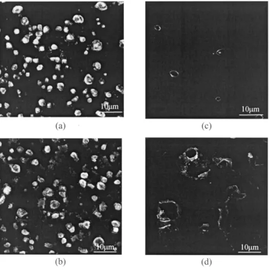
The SEM micrographs for the CoSi surface after removal of the Cu and TaN layers by the HNO H O (1 : 1) solution are shown in Fig. 5. After 700 C annealing, precipitates were found on the CoSi surface for the Cu–TaN (0% and 5%)–CoSi –Si samples as shown in Fig. 5(a) and (b), while the surface of CoSi remains intact for the Cu–TaN (10%)–CoSi –Si sample as shown in Fig. 5(c). This implies that the barrier capability of TaN layers against Cu diffusion in the Cu–TaN –CoSi –Si structure increased with increasing the N flow rate during the reactive sputtering. However, the 800 C thermal annealing [Fig. 5(d)] reveals precipitate formation on the CoSi surface for the Cu–TaN (10%)–CoSi –Si sample which is consistent with the results of sheet resistance measurement as shown in Fig. 4.
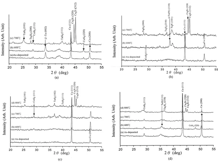
Fig. 6 shows the XRD spectra for the Cu–TaN –CoSi –Si samples subjected to anneal in N for 30 minute at various temperatures. For the TaN films deposited at the nitrogen flow ratio of 0% and 5%, the diffraction patterns reveal that the samples remain unchanged after anneal at temperatures up to 600 C, while different sets of peaks belonging to Cu Si, TaSi , and Ta Si are found after 700 C annealing as shown in Fig. 6(a) and (b). The cross-sectional TEM micrographs have showed that most of the Cu transported across the barrier and CoSi layers and reacted with Si substrate, resulting in the drastic increase of sheet resistance as shown in Fig. 4. In the meanwhile, the cross-sectional TEM measurement indicates that the CoSi layer did not dissociate during the process of the high-temperature annealing, implying the Si of Cu Si, TaSi , and Ta Si comes from the Si substrate. Another series of XRD patterns presented in Fig. 6(c) and (d) indicates the samples (TaN films deposited at the nitrogen flow ratio of 10% and 20%) remain unchanged after anneal at a temperature up to 700 C. But intermetallic compounds were also observed on the structure of Cu–TaN (10% 20%)–CoSi –Si samples after
Fig. 5. SEM micrographs of CoSi after removal of the Cu and TaN films from the Cu–TaN –CoSi –Si samples. The sputtered TaN films and the annealing temperatures are (a) TaN (0%), 700 C; (b) TaN (5%), 700 C; (c) TaN (10%), 700 C; and (d) TaN (10%), 800 C, respectively.
800 C annealing. The annealing temperatures resulted in the abrupt increase of sheet resistance as shown in Fig. 4, consistent with the results of SEM in Fig. 5. The results of Figs. 4 and 6 show that the annealing temperature before the Cu–CoSi –Si samples become unstable increased from 350 C to 600 C with the addition of a 50 nm thickness of TaN (0% 5%) as a barrier between Cu and CoSi . Increasing the nitrogen flow rate during the sputtering of TaN films will lead to a higher barrier capability of the TaN films and the failure annealing temperature for the Cu–TaN (10% 20%)–CoSi –Si samples is further increased to 700 C.
In our previous investigation [16], the XRD pattern for different Ta and TaN films deposited on (100) silicon substrate under different nitrogen flow rates follows the zone model, which progressively changed from voided columnar film of Ta, through fibrous of reduced grains [ –Ta(–N)], featureless structure (Ta N), and finally to columnar structure (TaN). The quasi-amorphous structure of –Ta(–N) films lengthen the diffusion path of Cu before it can react with Si, hence the TaN (3 5%) films provided a better barrier capability against Cu diffusion than those of TaN (0% and 10 30%) films [16]. Fig. 7 shows the XRD spectra of the TaN films deposited at the various nitrogen flow ratios on the CoSi film. Just like the TaN deposited on the Si, the crystallographic structure of TaN film deposited on the CoSi was also affected by
the nitrogen flow ratio during the reactive sputtering. In this figure, tetragonal –Ta is observed without any nitrogen flow. By incorporating nitrogen into the Ta films, the relatively low resistivity as measured from the four-point probe along with the phase identified by XRD patterns clearly indicates that the deposited films of nitrogen flow ratios of 3% and 5% are the low-resistivity –Ta phase and nitrogen-doped body-centered cubic (bcc) –Ta(–N) phases, respectively. The diffraction pattern for the films deposited at the nitrogen flow ration of 10, 15, and 20% respectively contains the high-resistivity face-centered cubic (fcc) TaN phase. In contrast to the TaN films deposited on the Si substrate, these patterns indicate that all the deposited films are not composed of an amorphous-like structure.
The bright-field image and selective area diffraction indi-cated that grain sizes of the TaN films deposited on the CoSi film decreased with the increased nitrogen flow ratio. Fig. 8(a) displays a transmission electron bright-field micrograph, taken from the diffuse ring of the diffraction pattern (inset) for –Ta films with grain size of 20 30 nm deposited without any nitrogen flow. On the contrary, the matrix exhibits a speckle feature of size 2 nm for TaN films deposited at 20% ni-trogen flow ratio [Fig. 8(b)]. The activation energies of the Cu diffusion in the TaN were measured to be 1.3 eV–2.7 eV, which indicated that the Cu diffusion in the TaN would be controlled
Fig. 6. XRD spectra for (a) Cu–TaN (0%)–CoSi –Si; (b) Cu–TaN (5%)–CoSi –Si; (c) Cu–TaN (10%)–CoSi –Si; and (d) Cu–TaN (20%)–CoSi –Si samples subjected to anneal at various temperatures.
Fig. 7. XRD spectra of the TaN deposited at the various nitrogen flow ratios on CoSi . The phase identified by XRD patterns indicates that the deposited films of nitrogen flow ratios of 0, 3, and 5% are the –Ta phase, –Ta phase, and nitrogen-doped bcc- –Ta(–N) phases, respectively. The diffraction pattern for the films deposited at the nitrogen flow ratios of 10, 15, and 20% respectively contains the fcc-TaN phase.
by grain boundaries and lattice diffusion [13]. Since the barrier layer allows Cu to preferentially penetrate through the grain
boundaries, a barrier structure with small grains increases the diffusion path of Cu to react with Si. Hence the TaN films deposited at the nitrogen flow ratio of 10% 20% yield the better barrier properties than those of 0% 5%.
As discussed in the Cu–CoSi /n –p junction diodes, the electrical characteristics are usually more sensitive than the metallurgical properties for the analysis of the reaction that occurred within the structure. Fig. 9 illustrates the re-verse-biased current densities of the Cu–TaN –CoSi /n –p junction diodes annealed at various temperatures. For the diodes without any heat treatment (as-deposited), the leakage current densities remain stable on the order of 10 A/cm . Nevertheless, the diode leakage increased with increasing the annealing temperature and all of diodes failed after annealing at 650 C. The abrupt increase of leakage current density in the 650 C-annealed diodes implies that the junctions were markedly destroyed even though no evidence of reaction can be found by the material analysis. As seen in Fig. 9, it is interesting that in the 600 C-annealed diode the barrier capability of TaN layer against Cu diffusion increased with increasing the nitrogen flow ratio. In other words, a 50-nm TaN (nitrogen flow ratio 10%) layer is observed to be an effective diffusion barrier up to 600 C between Cu and CoSi for maintaining the electrical integrity of the junction diodes. While at the
Fig. 8. Bright-field images of TaN films deposited at nitrogen flow ratio of (a) 0% and (b) 20%.
same annealing temperature, the diodes failed with the TaN diffusion barrier sputtered at the nitrogen flow ratios ranging from 0% to 5%. SIMS measurement was used to investigate the failure mechanism of the fabricated diodes. Results showed that an interdiffusion of Cu and Si across the barrier film is found for the Cu–Ta–CoSi –Si sample annealed at 600 C. The electrical evaluation reveals that this interdiffusion destroyed the junction characteristics as shown in Fig. 9. In addition, the SIMS analysis for the Cu–TaN (5%)–CoSi –Si sample annealed at 600 C showed that the relatively small amount of Cu atoms diffuses into the Si substrate as compared to the Cu–Ta–CoSi –Si sample. Although the small amount of Cu atoms diffused into Si substrate did not affect the Cu sheet re-sistance significantly (see Fig. 4), the junction leakage showed a three-order of magnitude increase in the leakage current
Fig. 9. Leakage current density of the Cu–TaN –CoSi /n –p junction diodes versus the annealing temperature. The TaN layer was reactively sputtered at the different nitrogen flow ratios.
measurement (from 10 to 10 A/cm , as seen in Fig. 9). Furthermore, SIMS measurement was also used to investigate the interdiffusion for the Cu–TaN ( 10%)–CoSi –Si samples annealed at 600 C. In the measurement, an insignificant penetration of Cu atoms through the barrier film resulted in the integrity of junction characteristics. The results of SIMS analysis are consistent with the electrical evaluations. They suggest that the barrier capability of TaN films against Cu diffusion increased with increased nitrogen-flow rate during the reactive sputtering. Again, it should be noticed that although increasing the nitrogen flow rate will lead to a higher barrier capability of the TaN layer against Cu diffusion, the high nitrogen ratio results in the high resistivity of the TaN films. From the XRD measurement and junction characterization, results show that the crystallographic structure and the barrier capability against Cu diffusion of TaN films are not only dependent on the nitrogen ratio but also on the substrate type.
IV. CONCLUSION
Metallurgical reaction in Cu–CoSi –Si structure was ob-served after a 400 C furnace annealing, while the electrical degradation of Cu–CoSi /n –p junction diodes was observed after annealing at 300 C. By using a 50 nm thickness of TaN layer as diffusion barrier, the Cu–TaN –CoSi /n –p junction diodes were able to sustain the 30 min thermal annealing up to 600 C without degrading the basic electrical characteristics. With a higher temperature annealing of 750 C, metallurgical reaction occurred in local spots with the formation of Cu Si, TaSi , and Ta Si . The high-temperature failure of barrier capability for the TaN layers is due to interdiffusion of Cu and Si across the TaN film structure and the interdiffusion is affected by the microstructure of the TaN films. By increasing the nitrogen flow ratio, the evolution of structure of the TaN films changes from pure –Ta through low-resistivity –Ta phase, nitrogen-doped body-centered cubic –Ta(–N) phase, and finally to small grain size face-centered cubic TaN phase. Among them, the small grain size face-centered cubic TaN
on the infrastructure during the deposition process.
ACKNOWLEDGMENT
The authors would like to thank the National Nano Device Laboratory, Hsinchu, Taiwan, R.O.C., for providing an excellent processing environment.
REFERENCES
[1] P. L. Shah, “Refractory metal gate processes for VLSI applications,” IEEE Trans. Electron Devices, vol. 26, pp. 631–640, Apr. 1979. [2] K. L. Wang, T. C. Holloway, R. F. Pinizzotto, Z. P. Sobczak, W. R.
Hunter, and A. F. Tasch, Jr., “Composite TiSi /n poly-Si low-resis-tivity gate electrode and interconnect for VLSI device technology,” IEEE Trans. Electron Devices, vol. 29, pp. 547–553, Apr. 1982. [3] S. P. Murarka, “Multilevel interconnections for ULSI and GSI era,”
Mater. Sci. Eng., vol. R19, pp. 87–151, 1997.
[4] M. M. Moslehi, A. Paranjpe, L. Velo, and T. Omstead, “Ultralarge scale integrated metallization and interconnects,” J. Vac. Sci. Technol., vol. A17, no. 4, pp. 1893–1897, 1999.
[5] C. Ryu, K.-W. Kwon, A. L. S. Loke, H. Lee, T. Nogami, V. M. Dubin, R. A. Kavari, G. W. Ray, and S. S. Wong, “Microstructure and reliability of copper interconnects,” IEEE Trans. Electron Devices, vol. 46, pp. 1113–1120, June 1999.
[6] S. Q. Hong, C. M. Comrie, S. W. Russell, and J. W. Mayer, “Phase forma-tion in Cu–Si and Cu–Ge,” J. Appl. Phys., vol. 70, no. 7, pp. 3655–3660, 1991.
[7] S. D. Brotherton, J. R. Ayres, A. Gill, H. W. van Kesteren, and F. J. A. M. Greidanus, “Deep levels of copper in silicon,” J. Appl. Phys., vol. 62, no. 5, pp. 1826–1832, 1987.
[8] F. La Via and E. Rimini, “Electrical characterization of ultra-shallow junctions formed by diffusion from a CoSi layer,” IEEE Trans. Electron Devices, vol. 44, pp. 526–534, Apr. 1997.
[9] J. O. Olowolafe, J. Li, B. Blanpain, and J. W. Mayer, “Interaction of Cu with CoSi with and without TiN barrier layers,” Appl. Phys. Lett., vol. 57, no. 13, pp. 1307–1309, 1990.
[10] J.-C. Chiou and M.-C. Chen, “Thermal stability of Cu–CoSi contacted p+n shallow junction with and without TiW diffusion barrier,” J. Elec-trochem. Soc., vol. 141, no. 10, pp. 2804–2810, 1994.
[11] H. Ono, T. Nakano, and T. Ohta, “Diffusion barrier effects of transition metals for Cu/M–Si multilayers (M= Cr, Ti, Nb, MO, Ta, W),” Appl. Phys. Lett., vol. 64, no. 12, pp. 1511–1533, 1994.
[12] J.-C. Chuang, S.-L. Tu, and M.-C. Chen, “Sputter-deposited Mo and re-actively sputter-deposited Mo–N films as barrier layers against Cu dif-fusion,” Thin Solid Films, vol. 346, pp. 299–306, 1999.
[13] T. Oku, E. Kawakami, M. Uekubo, K. Takahiro, S. Yamaguchi, and M. Murakami, “Diffusion barrier property of TaN between Si and Cu,” Appl. Surf. Sci., vol. 99, pp. 265–272, 1996.
[14] M. T. Wang, Y. C. Lin, and M. C. Chen, “Barrier properties of very thin Ta and TaN layers against copper diffusion,” J. Electrochem. Soc., vol. 145, pp. 2538–2545, 1998.
in electronics from NCTU, in 1987 and 1992, respectively.
In 1993, he joined the Faculty of Feng Chia Uni-versity, Taichung, Taiwan, where he is now a Pro-fessor and Chairman with the Institute and Depart-ment of Electronic Engineering. He is interested in fabrication process in deep submicrometer VLSIs, thin-gate dielectrics, ultra-shallow junctions, metal silicides, and multilevel interconnections. He is cur-rently developing the Si–Ge gate engineering and the integration of Cu metal-lization and ultrashallow junctions. He is a Patent Examiner with the Intellectual Property Office, Ministry of Economic Affairs, Taiwan.
Dr. Yang has been Editor of the Journal of Vacuum Science Technology since 1999 and is a member of the Vacuum Science Technology Society, Taiwan.
Wen-Fa Wu was born in Kaohsiung, Taiwan,
R.O.C., in 1967. He received the B.S. degree in electronics engineering from National Chiao Tung University, Hsinchu, Taiwan, in 1990, and the Ph.D. degree from Institute of Electronics, National Chiao Tung University, in 1994.
He joined the National Nano Device Laboratories (NDL), Hsinchu, as an Associate Researcher since 1994. He is engaged in developing metallization tech-nology on IC manufacturing. His research interests include conductor systems of Cu and Al metalliza-tion, salicide technology, electromigration and stress migrametalliza-tion, and integration of Cu and low-k dielectrics.
Hsin Chiang You was born in Changhua, Taiwan,
R.O.C., on May 23, 1977. He received the B.S. and M.S. degrees in electrical engineering from Feng Chia University, Taichung, Taiwan, in 1999 and 2001, respectively. He is currently pursuing the Ph.D. degree at National Chiao-Tung University, Hsinchu, Taiwan.
His research interests include the integration of Cu metallization, electronic materials analyses, and ad-vanced photolithography technologies.
Keng-Laing Ou was born in Kaoshiung, Taiwan,
R.O.C., on December 6, 1973. He received the B.S. degree from the Department of Mechanical Engineering, and the M.S. degree in material science and engineering and mechanical engineering from National Chiao-Tung University, Hsinchu, Taiwan, in 1995 and 1997, respectively, where he is currently pursuing the Ph.D. degree.
His research includes the integration of Cu metal-lization, electronic materials analyses, and thin-film technologies.
Tan Fu Lei (M’98) was born in Keelung, Taiwan,
R.O.C., on September 17, 1944. He received the B.S. degree in electrical engineering from National Cheng Kung University, Tainan, Taiwan, in 1967, and the M.S. and Ph.D. degrees in electronics engineering from National Chiao Tung University, Hsinchu, Taiwan, in 1970 and 1979, respectively.
From 1970 to 1972, he was with the Fine Products Microelectronics Corporation, Taiwan, as an Engi-neer working on the fabrication of small-signal tran-sistors. From 1980 to 1982, he was the Plant Man-ager, Photronic Corporation, Taiwan. In 1983, he joined the Faculty at National Chiao Tung University as an Associate Professor with the Department of Elec-tronics Engineering and the Institute of ElecElec-tronics. From 1984 to 1986, he was the Director of the Semiconductor Research Center. From 1991 to 1998, he also was the Deputy Director of the National Nano Device Laboratory. Presently, he is a Professor with the Department of Electronics Engineering and the Institute of Electronics. His research interests are semiconductor devices and VLSI tech-nologies.
Chang-Pin Chou received the B.S. degree in physics
from Fu Jen University, Taiwan, R.O.C., in 1971, and the M.S. degree in physics from Montana State University, Bozeman, in 1973. He then received the M.S. and Ph.D. degrees in material science and engineering from the University of Tennessee, Knoxville, in 1975 and 1978, respectively.
Since 1983, he has been a Professor with the Department of Mechanical Engineering, National Chiao-Tung University, Hsinchu, Taiwan. In 1989 and 1990, he was an International Fellow with the Department of Materials, Stanford Research Institute, Stanford, CA. He has conducted research in welding design, weldability testing, automated and robotic welding, and failure analysis. His present research interests include MEMS fabrication, thin-film materials and analyses, interconnection reliability in metallization, micro weldability, and heat treatment of metal alloys.