互補式金氧半8位元40MHz取樣頻率管線化類比至數位轉換器之設計與分析
68
0
0
全文
(2) 互補式金氧半八位元 40MHz 取樣頻率管線化 類比至數位轉換器之設計與分析. The Design and Analysis of a CMOS 8bit 40MS/s Pipelined Analog-to-Digital Converter 研 究 生:陳正瑞 指導教授:吳錦川 教授. Student: Cheng-Jui Chen Advisor: Prof. Jiin-Chuan Wu. 國立交通大學 電子工程學系 電子研究所碩士班 碩士論文 A Thesis Submitted to Institute of Electronics College of Electrical Engineering and Computer Science National Chiao Tung University In Partial Fulfillment of the Requirements for the Degree of Master of Science in Electronic Engineering May 2004 Hsin-Chu, Taiwan, Republic of China.
(3) 互補式金氧半八位元 40MHz 取樣頻率管線化 類比至數位轉換器之設計與分析 學生:陳正瑞. 指導教授:吳錦川教授. 國立交通大學電子工程學系 電子研究所碩士班. 摘要. 本論文先對管線化類比至數位轉換器的架構加以描述,並同時將管線化 類比至數位轉換器所可能造成誤差的原因加以探討,並提出解決方法。 本論文描述一個 3.3V,8 位元,40M sample/s 管線化的類比至數位轉換 器。本設計採用每級 1.5 位元的架構並運用數位錯誤修正的技術。主要的 元件:餘數放大器(residue amplifier),比較器(comparator),正反 器(D-flip-flop),加法器(adder)和時脈產生器(clock generator)。 整個電路是由七級加上一個前端輸入保持電路所組成,全差動輸入範圍為 -1V~+1V。餘數放大器的部分是以開關加電容配合放大器來實現。比較器的 部分是以開關加電容配合動態比較器來實現。本架構多加入了一個不同相 位的時脈,以減少比較器對餘數放大器的雜訊干擾,及確保比較器得到正確 的值。 本架構使用台積電 0.35um 2P4M 互補式金氧半的製程,並以混合訊號全 客戶式佈局實現。整個晶片佈局面積 1.8mm x 1.8mm。以 HSPICE 作模擬, 模擬的結果符合 8 位元解析度,40MHz 取樣頻率,總功率消耗約為 40mW。 i.
(4) The Design and Analysis of a CMOS 8bit 40MS/s Pipelined Analog-to-Digital Converter Student: Cheng-Jui Chen. Advisor: Prof. Jiin-Chuan Wu. Department of Electronics Engineering & Institute of Electronics National Chiao-Tung University. ABSTRACT In this thesis, the advantage and the architecture of the pipelined analog-to-digital converter (ADC) is described. Furthermore, the error source of the pipelined ADC is shown and discussed. And there are some solutions to these problems in this thesis.. We also illustrate a 3.3V, 8-bit, 40M sample/s CMOS pipelined ADC. The 1.5b/stage architecture with digital error correction is used in this ADC. The component in the ADC is the residue amplifier, the comparator, the D flip-flop, the adder and the clock generator. The ADC has 7 stages and a front-end sample-and-hold(S/H). The input is a fully differential format, the input range is -1V~+1V. The residue amplifier is implemented by the switch capacitor circuit. The comparator is implemented by the switch and capacitor and dynamic comparator. We add a new phase of clock to reduce the noise in residue amplifier from comparator.. The ADC was designed using TSMC 0.35um 2P4M CMOS process and mixed-signal full custom layout is applied. The chip area is 1.8mm x 1.8mm. The simulation is done by HSPICE. The specification of the ADC is 8bit resolution, 40M sampling rate, less than 40mW power consumption. ii.
(5) 誌. 謝. 首先要感謝指導教授吳錦川博士讓我有機會加入老師的研究群, 並對老師在我兩年研究所其間所提供的細心指導表示感謝。. 感謝奈米電子與晶片系統實驗室裡所有的學長姐跟同學們這兩 年來的照顧。特別謝謝林子超,黃鈞正,范啟葳,廖以義,陳志 熒,王文傑,歐陽銘,范姜朝馨,蘇芳德學長在電路設計以及佈 局規劃上的指導,以及在晶片量測上所給予的寶貴意見,讓我可以 順利的完成這篇論文。除此之外,感謝同窗史周,權哲,棋樺, 聖文,瑋仁,阿嵐,在這兩年研究生的生涯中陪伴我一起成長並 給我許多幫助,感謝你們。 感謝我的女友淑惠,性人,小雞,阿胖,祥哥,芳吟,煒明, 馬亭,傑堯,耀中,在我最低潮的時候給我加油打氣,讓我能夠 有堅持下去的信念。. 感謝我的家人,沒有你們的後盾,就沒有今日的我,謝謝你們。. 謹以此篇論文獻給所有關心我的人. 正瑞 於 新竹交大 筆. iii.
(6) CONTENTS CHINESE ABSTRACT…………………………………………….. i ENGLISH ABSTRACT……………………………………………. ii ACKNOWLEDGEMENTS………………………………………..iii CONTENTS……………………………………………………….. iv TABLE CAPTION……………………………………………….. vii FIGURE CAPTIONS……………………………………………..viii CHAPTER 1 INTRODUCTION 1.1 Motivation and Goals……………………………………. 1 1.2 Thesis Organization……………………………………… 2 CHAPTER 2 Fundamentals 2.1 Overview………………………………………………… 3 2.1.1 Delta-Sigma Architecture……………………………. 5 2.1.2 SAR Architecture……………………………………. 5 2.1.3 Flash Architecture…………………………………….6 2.1.4 Pipeline Architecture………………………………… 7 2.1.5 A Simple ADC Comparison Matrix…………………. 8 2.2 Pipeline ADC versus Other ADCs………………………. 9 2.2.1 Versus the Delta-Sigma……………………………… 9 2.2.2 Versus SAR………………………………………….. 9 2.2.3 Versus Flash……………………………………….. 10 2.2.4 Conclusion………………………………………….. 10 2.3 Architecture for 8-bit 40MHz ADC……………………. 11 2.3.1 Architecture………………………………………… 11 2.3.2 Timing Strategy…………………………………….. 13 2.3.3 Digital Error Correction……………………………. 14 2.4 Non-ideality of Considerations………………………... 16. iv.
(7) CHAPTER 3 Circuit Design 3.1 Sample-and-Hold……………………………………… 17 3.1.1 Capacitors………………………………………….. 18 3.1.2 Op-amp Gain Requirement………………………… 19 3.1.3 Op-amp Bandwidth Requirement…………………... 20 3.1.4 Switches……………………………………………..22 3.2 Multiplying DAC………………………………………..22 3.3 Op-amp…………………………………………………. 25 3.4 Comparator…………………………………………….. 27 3.5 Digital Error Correction…………………………………30 3.6 Clock Generator………………………………………....32 3.7 Simulation……………………………………………….33 3.7.1 Simulation results of op-amp………………………..33 3.7.2 Simulation results of S/H……………………………33 3.7.3 Simulation results of MDAC……………………….. 34 3.7.4 Simulation results of clock generator………………. 35 3.7.5 Simulation results of whole chip…………………… 36 CHAPTER 4 Implementation and Results 4.1 Layout consideration…………………………………. 37 4.1.1 Transistor matching………………………………… 38 4.1.2 Capacitor…………………………………………….38 4.1.3 Floor Plan…………………………………………... 40 4.2 Performance…………………………………………...43 4.2.1 Dynamic……………………………………………. 43 4.2.2 Static………………………………………………... 44 4.3 Test setup…………………………………………….. 46 4.3.1 PC board design……………………………………..46 4.3.2 Instrument setup….………………………………… 48 4.4 Test result…………………………………………….. 51 v.
(8) 4.4.1 DC measurement…………………………………… 51 4.4.2 Discussion…………………………………………...52 CHAPTER 5 Conclusions 5.1 Conclusion………………………………………………. 54 5.2 Future work………………………………………………55 REFERENCES……………………………………………………..56 VITA………………………………………………………………...58. vi.
(9) TABLE CAPTIONS Table.2.1. ADC Comparison Matrix…………………………………………………..8. Table.3.1 Table.3.2 Table.4.1 Table.4.2. The requirements of Op-amp in S/H and MDAC……………………….25 Post-simulation results of op-amp………………………………………..33 Pin assignments……………………………………………………………42 Codes distribution…………………………………………………………52. vii.
(10) FIGURE CAPTIONS Fig.2.1 The requirements of ADC versus the fields of application……………………..4 Fig.2.2 The properties of different architectures……………………………………….. 4 Fig.2.3 Delta-Sigma Architecture………………………………………………………...5 Fig.2.4 SAR Architecture…………………………………………………………………6 Fig.2.5 Pipeline Arechitecture……………………………………………………………7 Fig.2.6 Architecture of 8-bit Pipeline ADC…………………………………………….12 Fig.2.7 Main Stage Circuit and Transfer Curve……………………………………….13 Fig.2.8. Clock Waveform…………………………………………………………………14 Fig.2.9 Example of Design Error Correction: First stage to Next Stage……………..15 Fig.3.1 Schematic diagram of sample-and-hold………………………………………..18 Fig.3.2 Op-amp gain requirement………………………………………………………20 Fig.3.3 Settling time of S/H………………………………………………………………21 Fig.3.4 Switches of S/H in Sample mode……………………………………………….. 22 Fig.3.5 Schematic diagram of MDAC…………………………………………………..23 Fig.3.6 Operation of MDAC…………………………………………………………….24 Fig.3.7 Telescopic op-amp……………………………………………………………….26 Fig.3.8 Common-mode feedback………………………………………………………..26 Fig.3.9 Telescopic op-amp with bias circuit……………………………………………27 Fig.3.10 Dynamic comparator……………………………………………………………. 28 Fig.3.11 Switch-capacitor differential comparator……………………………………..29 Fig.3.12 ADSC of the first 6 stages………………………………………………………30 Fig.3.13 ADSC of the final stage…………………………………………………………30 Fig.3.14 Registers and digital error correction logic……………………………………31 Fig.3.15 Digital error correction………………………………………………………….31 Fig.3.16 Clcok generator…………………………………………………………………..32 Fig.3.17 S/H FFT test………………………………………………………………………34 Fig.3.18 Transfer curve of MDAC……...………………………………………………... 35 Fig.3.19 Waveform of clock generator…………………………………………………... 35 Fig.3.20 Whole chip FFT test……………………………………………………………...36 Fig.4.1 Multi-finger transistor……………………………………………………………38 Fig.4.2 Common-centroid structure……………………………………………………...39 Fig.4.3 Layout of matched capacitors……………………………………………………40 Fig.4.4 Layout and floor plan of whole chip…………………………………………….41 Fig.4.5 Pin configuration………………………………………………………………….42 Fig.4.6 Sinusoidal histogram for an ideal ADC…………………………………………44 Fig.4.7 PCB block diagram………………………………………………………………46 Fig.4.8 Input signal and input termination circuit……………………………………...47 Fig.4.9 Reference voltage generate circuit………………………………………………47 Fig.4.10 Measurement setup………………………………………………………………48 Fig.4.11 Die photo………………………………………………………………………….49 Fig.4.12 PCB photo…………………………………………………………………………50 Fig.4.13 Codes distribution……………………………………………………………….. 51 Fig.4.14 The original bias circuit…………………………………………………………. 53 Fig.4.15 The improved bias circuit……………………………………………………....... 53. viii.
(11) Chapter1. Introduction. 1.1 Motivation and Goals With the continuous advance of semiconductor technology and scaling of devices, digital circuits have achieved both high speed and low power dissipation. This trend has several impacts on mixed-signal integrated circuits. In the first place, more operations are performed by digital circuits rather than by analog circuits. In the second place, the speed of the A/D and D/A interfaces must scale with the speed of the digital circuits in order to fully utilize the advantages of advanced technologies. With the trend of higher speed and lower power supply in VLSI system, the speed and resolution of ADC often appear as the bottleneck in data processing application. Moreover, the ADC is implemented on a chip with a great deal of digital circuit. The noise immunity of ADC becomes an important issue in mixed-signal processing systems. The goal of this research is to develop a high speed and high resolution ADC in standard CMOS technology. Such A/D converters find wide applications in battery powered instruments and low cost digital oscilloscopes.. 1.
(12) 1.2 Thesis Organization In Chapter 2, several A/D converters are reviewed. The architecture of the proposed pipelined ADC is also presented. In Chapter 3, the design and analysis of the circuits in each building block will be described. In Chapter 4, the layout consideration and floor plan will be presented. In Chapter 5, the measurement results of the fabricated pipelined A/D converter will be presented. In Chapter 6, the conclusion and perspectives are presented.. 2.
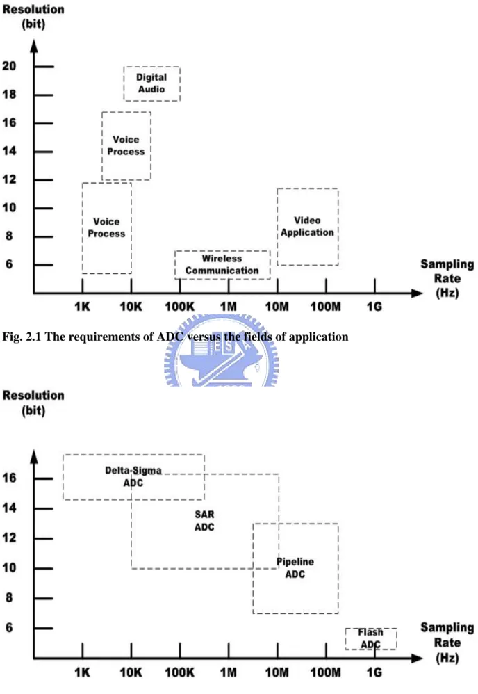
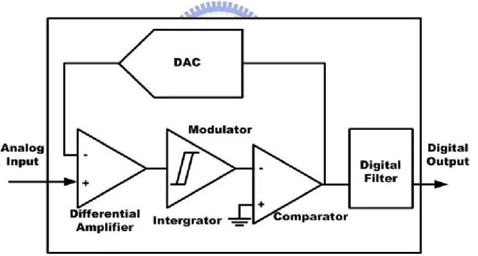
(13) Chapter 2. Fundamentals. 2.1 Overview [1] Analog-to-Digital converters find wide applications in many fields. There are several architectures for different applications. The requirements of ADC versus different fields of application are shown in Fig. 2.1. The properties of different architectures are shown in Fig. 2.2. In Fig. 2.2, there are many kinds of Nyquest A/D converter architectures. Some converters are suitable for high resolution and some are used for high-speed application. Here, we briefly discuss operation and characteristics of these architectures as follows.. 3.
(14) Fig. 2.1 The requirements of ADC versus the fields of application. Fig. 2.2 The properties of different architectures. 4.
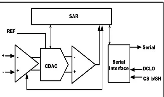
(15) 2.1.1 Delta-Sigma Architecture Delta-Sigma ADC is based on the principle of highly over-sampling the input signal followed by a digital filter/decimator to obtain the digital code equivalent. Delta-Sigma ADC is ideal for low-bandwidth signals and is capable of very high resolution, 16- to 24-bits. This converter technology allows for a trade-off between signal bandwidth and resolution that is often externally programmable. A digital filter can have greater complexity than its analog equivalent at lower cost, and is always exactly reproducible over temperature and time. Complex filter functions (i.e. 50-/60-Hz notch filter) are readily achieved and are often tailored to a specific application. Applications for Delta-Sigma ADCs include industrial process control, analytical and test instrumentation, medical imaging and acquisition, communications, and professional and consumer audio. DSP compatibility makes them ideal choices for system solutions.. Fig. 2.3 Delta-Sigma architecture. 2.1.2 SAR Architecture SAR-type converters are frequently the architecture of choice for medium-to–highresolution applications with medium sampling rates. SAR ADCs most commonly range in 5.
(16) resolution from 10- to 16-bits. They provide low power consumption and a small form factor. A SAR has little sample-to-conversion latency compared to a pipeline or delta-sigma converter. This combination makes them ideal for real-time applications such as industrial control, motor control, power management, portable/ battery-powered instruments, PDA, test equipment and data/signal acquisition. In a successive approximation register (SAR) ADC, the bits are decided by a single high-speed, high-accuracy comparator bit by bit, from the MSB down to the LSB. This is done by comparing the analog input with a DAC whose output is updated by previously decided bits and successively approximates the analog input.. Fig. 2.4 SAR Architecture. 2.1.3 Flash Architecture Flash analog-to-digital converters, also known as parallel ADCs, are the fastest way to convert an analog signal to a digital signal. They are suitable for applications requiring very large bandwidths. However, flash converters consume a lot of power, have relatively low resolution, and can be quite expensive. This limits them to high frequency applications that typically cannot be addressed any other way. Examples include data acquisition,, satellite 6.
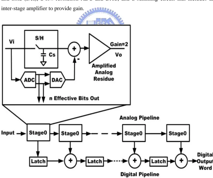
(17) communication, radar processing, sampling oscilloscopes, and high-density disk drives.. 2.1.4 Pipeline Architecture This converter type offers high speed, high resolution and excellent performance, along with modest levels of power dissipation and small die size. Within reasonable design limits, they also offer excellent dynamic performance. Pipeline latency is typically six or more clock cycles. Target applications for pipeline ADCs include CCD-based imaging systems, ultrasonic medical imaging, digital receiver, base station, digital video, xDSL, cable modem and fast Ethernet. Additionally, communication systems in which total harmonic distortion (THD), spurious-free dynamic range (SFDR) and other frequency-domain specifications are significant. Pipeline ADCs consist of numerous consecutive stages, each containing a sample and hold (S/H), a low-resolution ADC and DAC, and a summing circuit that includes an inter-stage amplifier to provide gain.. Fig. 2.5 Pipeline Architecture 7.
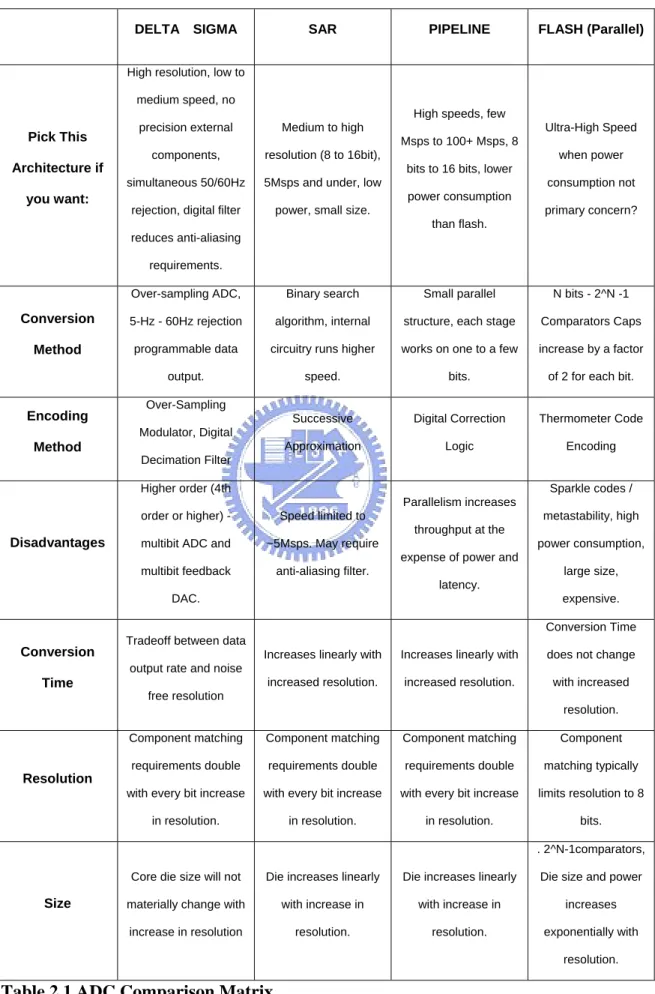
(18) 2.1.5 A Simple ADC Comparison Matrix [2] DELTA SIGMA. SAR. PIPELINE. FLASH (Parallel). High resolution, low to medium speed, no High speeds, few. Pick This. precision external. Medium to high. components,. resolution (8 to 16bit),. Architecture if. when power bits to 16 bits, lower. simultaneous 50/60Hz. you want:. Ultra-High Speed Msps to 100+ Msps, 8. 5Msps and under, low. consumption not power consumption. rejection, digital filter. power, small size.. primary concern? than flash.. reduces anti-aliasing requirements. Over-sampling ADC,. Binary search. Small parallel. N bits - 2^N -1. Conversion. 5-Hz - 60Hz rejection. algorithm, internal. structure, each stage. Comparators Caps. Method. programmable data. circuitry runs higher. works on one to a few. increase by a factor. output.. speed.. bits.. of 2 for each bit.. Successive. Digital Correction. Thermometer Code. Approximation. Logic. Encoding. Encoding. Over-Sampling Modulator, Digital. Method Decimation Filter Higher order (4th. Sparkle codes / Parallelism increases. order or higher) -. metastability, high. Speed limited to throughput at the. Disadvantages. multibit ADC and. ~5Msps. May require. power consumption, expense of power and. multibit feedback. anti-aliasing filter.. large size, latency.. DAC.. expensive. Conversion Time. Conversion. Tradeoff between data Increases linearly with. Increases linearly with. does not change. increased resolution.. increased resolution.. with increased. output rate and noise. Time free resolution. resolution. Component matching. Component matching. Component matching. Component. requirements double. requirements double. requirements double. matching typically. with every bit increase. with every bit increase. with every bit increase. limits resolution to 8. in resolution.. in resolution.. in resolution.. bits.. Resolution. . 2^N-1comparators,. Size. Core die size will not. Die increases linearly. Die increases linearly. Die size and power. materially change with. with increase in. with increase in. increases. increase in resolution. resolution.. resolution.. exponentially with resolution.. Table 2.1 ADC Comparison Matrix 8.
(19) 2.2 Pipeline ADC versus Other ADCs 2.2.1 Versus the Delta-Sigma. Traditionally, over-sampling/delta-sigma-type converters commonly used in digital audio have a limited bandwidth of about 22 KHz or so. But recently some high-bandwidth delta-sigma -type converters have reached a bandwidth of 1MHz to 2MHz with 12 to 16 bits of resolution. These are usually very-high-order delta-sigma modulators (for example, fourth or even higher) incorporating a multi-bit ADC and multi-bit feedback DAC, and their main applications are in ADSL. Delta-sigma converters have the innate nature of requiring no special trimming/calibration, even for 16 to 18 bits of resolution. They also require no steep rolling-off anti-alias filter at the analog inputs, because the sampling rate is much higher than the effective bandwidth; the backend digital filters take care of it. The over-sampling nature of the delta-sigma converter also tends to "average out" any system noise at the analog inputs. However, sigma-delta converters trade speed for resolution. The need to sample many times (for example, at least 16 times, but often much higher) to produce one final sample causes the internal analog components in the delta-sigma modulator to operate much faster than the final data rate. The digital decimation filter is also nontrivial to design and takes up a lot of silicon area. The fastest, high-resolution delta-sigma-type converters are not expected to have more than a few MHz of bandwidth in the near future. Like pipelined ADCs, delta-sigma converters also have latency.. 2.2.2 Versus SAR In a successive approximation register (SAR) ADC, the bits are decided by a single high-speed, high-accuracy comparator bit by bit, from the MSB down to the LSB, by comparing the analog input with a DAC whose output is updated by previously decided bits and successively approximates the analog input. This serial nature of SAR limits its operating speed to no more than a few MS/s, and still slower for very high resolutions (14 to 16bits). A. 9.
(20) pipelined ADC, however, employs a parallel structure in which each stage works on 1 to a few bits (of successive samples) concurrently. Although there is only one comparator in a SAR, this comparator has to be fast (clocked at approximately the number of bits x the sample rate) and as accurate as the ADC itself. In contrast, none of the comparators inside a pipelined ADC needs this kind of speed or accuracy. However, a pipelined ADC generally takes up significantly more silicon area than an equivalent SAR. A SAR also displays a latency of only one cycle, versus about N (N: number of bit) cycles in a typical pipeline. Like a pipeline, a SAR with more than 12 bits of accuracy usually requires some form of trimming or calibration.. 2.2.3 Versus Flash. Despite the inherent parallelism, a pipelined ADC still requires accurate analog amplification in DACs and inter-stage gain amplifiers, and thus significant linear settling time. A purely flash ADC, on the other hand, has a large bank of comparators, each consisting of wideband, low-gain preamps followed by a latch. The preamps, unlike those amplifiers in a pipelined ADC, need to provide gains that don't even have to be linear or accurate earning, only the comparators' trip points have to be accurate. As a result, a pipelined ADC cannot match the speed of a well-designed flash ADC. Although extremely fast 8-bit flash ADCs (or their folding/interpolation variants) exist with sampling rates as high as 1.5GS/s, it is much harder to find a 10-bit flash, while 12-bit (or above) flash ADCs are not commercially viable products. This is simply because in a flash the number of comparators goes up by a factor of 2 for every extra bit of resolution, and at the same time each comparator has to be twice as accurate. In a pipeline, however, to a first order the complexity only increases linearly with the resolution, not exponentially. At sampling rates obtainable by both a pipeline and a flash, a pipelined ADC tends to have much lower power consumption than a flash. A pipeline also tends to be less susceptible to comparator meta-stability. Comparator meta-stability in a flash can lead to sparkle-code errors (a condition in which the ADC provides unpredictable, erratic conversion results).. 2.2.4 Conclusion 10.
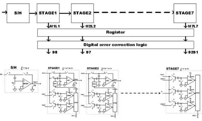
(21) The pipelined ADC is the architecture of choice for sampling rates from a few MS/s up to 100MS/s+. Complexity goes up only linearly (not exponentially) with the number of bits, providing converters with high speed, high resolution, and low power at the same time. They are very useful for a wide range of applications, most notably in the digital communication area, where a converter's dynamic performance is often more important than traditional DC specifications like differential nonlinearity (DNL) and integral nonlinearity (INL). Their data latency is of little concern in most applications [3].. 2.3 Architecture for 8-bit 40MHz ADC 2.3.1 Architecture [4][5] The block diagram of a typical pipelined ADC is shown in Fig. 2.6. All of the pipelined stages are similar in structure. Each stage consists of a sample-and-hold amplifier, a Digital-to-Analog converter (DAC), a low resolution Analog-to-Digital sub-converter (ADSC), a subtractor, and a fix-gain amplifier. The beginning sample-and-hold relaxes the timing requirements of the first stage during its sampling phase by holding the instantaneous value of the analog input. Following the S/H, each stage samples and holds the output signals of the previous stage. The signal is coarsely quantized by the ADSC to produce the first 1 MSB’s and 1 bit for digital error correction. Then using a DAC, the quantized value is subtracted from original input signal to yield the output residue. For the output signal range is the same with the input signal range for each stage, this is made by the amplifier with gain of 2. The resulting residue signal is applied to the next stage for finer conversion on the next clock cycle. The function of the D/A, the subtraction, and the amplification of the remainder are combined into one single circuit called the multiplying DAC (MDAC). The last stage consists of a 2-bits flash ADC, and a thermometer-code-to-binary-code combinational logic.. 11.
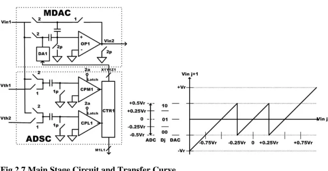
(22) Fig. 2.6 Architecture of 8-bit Pipeline ADC. After the signal has propagated through 8 stages, one complete conversion is produced. The total digital outputs from all stages are 14 bits. These operations work concurrently and enable the pipelined architecture to achieve a high throughput. The digital codes ate overlapped by 1 bit to perform digital error correction. Therefore, the total 14 bits from all stages are delayed properly and produced 8 bits [6][7]. Although a single-ended configuration is shown for simplicity, the actual implementation was fully differential. The conceptual circuit of main stages of pipeline is shown in Fig. 2.7. The MDAC with SC configuration performs sample-and-hold function, DAC, subtraction and multiply by 2 functions. The ADSC consists of two flash converters. The input is sampled by the frontier S/H circuit to convert the analog signal to the two differential dc signal input. Then, the signal is compared by two comparators to decide where it is located on the residue chart. The decision level is ± 1 / 4Vr (Vr: full swing of input voltage). The output digital codes are latched by the D-flip-flop which is used for doing pipeline. Because each stage’s output does not come out at the same time, we have to use flip-flop to latch them. From Fig.2.7, we can realize that the MDAC only needs to decide 3 conditions 2Vin-Vr, 2Vin, or 2Vin+Vr. The MDAC’s output is the next stage’s input. When the input signal is applied, each stage samples and quantizes, subtracts the quantized analog output signal of DAC, and passes the residue to the next stage with amplification for finer conversion. Every stage can get 2-bit digital output 12.
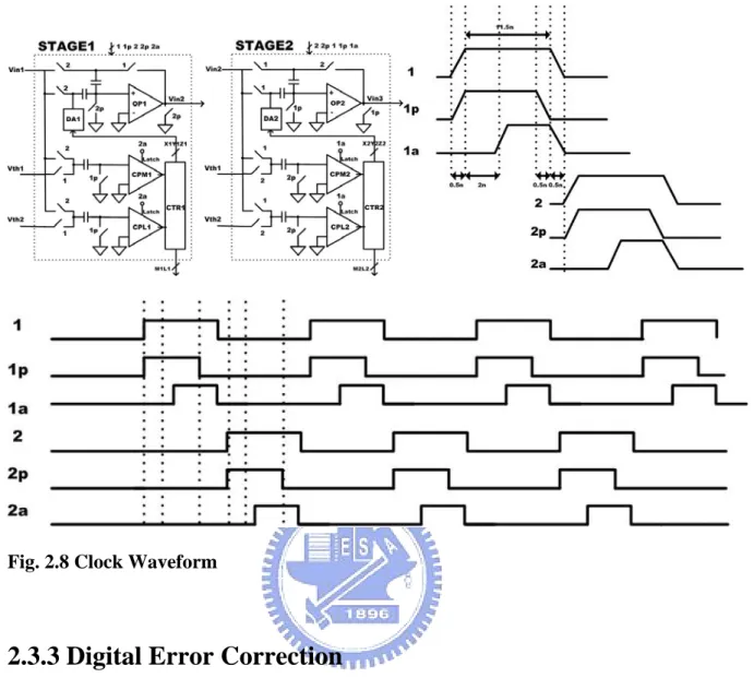
(23) 00, 01 and 10, and be latched in to the pipeline path.. Fig 2.7 Main Stage Circuit and Transfer Curve. 2.3.2 Timing Strategy The design of our residue amplify circuit is a switch-capacitor S/H structure as shown in Fig.2.8. The basic ideal of switch-capacitor circuit is the charge transfer. The important issue is to transfer the charge totally without loss. Thus, two non-overlap clock phases clk1 clk2 are required. In order to cancel out the charge injection error, the fully differential structure and the bottom-plate technique is used in the residue amplify circuit. This will need two more advanced clock phases clk1p clk2p. For example, the clk1p control the switches on the top-plate of sample capacitors and turn off earlier before the switches on the bottom-plate so that the charge injection is signal independent. The addition phases, clk1a and clk2a, are needed for the ASDC. To avoid the noise being compared by comparators in the beginning of transferring, the comparator will start comparing until the charge redistribution has been finished and stabilized. The waveform is shown in Fig. 2.8.. 13.
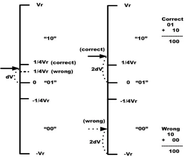
(24) Fig. 2.8 Clock Waveform. 2.3.3 Digital Error Correction Digital error correction is the name of the calibration technique that reduces the gain, keeps the voltage range constant with modified coding and tolerates greater comparator offset. A conceptual transfer function is shown in Fig.2.9. This kind of digital error correction is called the 1.5bit/stage algorithm. The comparator thresholds (ADSC) are at 1/4Vr and -1/4Vr; the DAC levels are at -1/2Vr, 0 and 1/2Vr. The codes are shown on top of the transfer function and the over-ranging part on the transfer function will be digitally corrected by the next stage except the last stage of the pipeline. The 1.5-bit/stage here represents the effective bits per stage after digital correction [8]. We can get 2-bit in each stage. The second bit is used for correction. When the input is less than the negative decision level, -1/4Vr, we simply get a 0 in the first bit and give another 0 in the second bit. The second bit is 0 means that no need to add 1 to the first bit. In the same way, when the input is greater than the positive decision level, +1/4Vr, we can get a 1 in the first bit and give another 0 in the second bit, meaning that 14.
(25) no need to get a 1 in the first bit and give another 0 in the second bit. When the input is in the un-distinguished region between -1/4Vr and +1/4Vr, we give a 0 in the first bit and give a 1 in the second bit. We can get 0 in this stage and residue is 2xVin. In the next stage, if the input is positive, then the first bit will be corrected because it will get a “10”. If the input is negative, then the next stage will get a “00”. And there is no need to change the “0” bit in the first stage. The amplified residue remains within the conversion range of the next stage when the ADSC nonlinearity is between ± 1 / 2 LSB . Under these conditions, errors caused by the ADSC nonlinearity less than 1/2 LSB can be corrected. For example, see from Fig.2.9 when the input is in the “10” region and very close to the “01” region. If the comparator is wrong and decides the input as “01”. Then it will produce a residue of 2Vin. The residue voltage is the same as the real value, that it won’t affect the next few stages. And we can correct this bit by adding one to “01”.. Fig. 2.9 Example of Digital Error Correction: First Stage to Next Stage. 15.
(26) 2.4 Non-ideality of Considerations Charge Injection Error [8]. MOS switches introduce a significant amount of error due to the channel charge stored in the MOSFET device. The charge in the conductance channel is approximately Cox(Vgs − Vth) . When the MOS switch is turned off, the amount of channel charge injected into the sampling capacitor represents an error source as a result of the sudden release of the charge under the MOS gate. The additional charge will cause a large error in the high resolution Switch-Capacitor circuit.. Clock Feed-through. The effect of clock feed-through is due to the gate-drain, gate-source parasitic capacitor.. Offset Error [9]. The offset error in a pipelined ADC results from the charge injection of reference switches and the mismatch of differential pairs.. Gain Error. The finite op-amp gain and the capacitor mismatch are the two major gain errors. The finite op-amp gain makes the settled voltage can’t reach the target level.. 16.
(27) Chapter3. Circuit Design. 3.1 Sample-and-Hold[9][10] The most important and performance dominating circuit in the pipelined ADC is the input stage sample-and-hold (S/H) amplifier. Fig.3.1 shows the schematic diagram of the unity-gain S/H. The signal ground Vmid is the common-mode voltage of the output differential signal. The architecture of the op-amp is a telescopic amplifier, which has an input common-mode voltage at 1.2V and an output common-mode voltage at 1.5V. The clock1, clock1p are used during the sample phase and clock2 is used during the hold phase. The clock1 and clock2 are non-overlap phases to prevent the charge loss on the path when both the clocks are at high level. The clock1p has the same rising edge to the clock1 phase, but the earlier falling edge takes the advantage of reducing the charge injection from the sampling switches. There is a switch connects output nodes during the sample phase, and then keeps the voltage of output nodes at the output common-mode and prevent saturation. That reduces the settling time when a non-saturated voltage needs to go back to the target voltage at hold phase. 17.
(28) Fig.3.1 Schematic diagram of sample-and-hold. 3.1.1 Capacitors [11] A certain minimum signal capacitor size is needed to maintain adequate noise performance and dynamic range. The SNR (signal to noise ratio) is calculated as. ⎛ ⎜ 2 ⎛ VR ⎞ ⎜ ⎟ ⎜ ⎞ ⎛ ⎜ 2⎠ ⎜ VR ⎟ ⎝ SNR = 20 log⎜ 2 ⎟⎟ = 10 log⎜ ⎜ V 2 ⎜ ⎛ ⎞ R ⎝V N⎠ ⎜ KT ⎜ 2 N ⎟ ⎠ ⎜3 +⎝ 12 ⎝ C. ⎞ ⎟ ⎟ ⎟ ⎟ ⎟ ⎟ ⎟ ⎠. (1). where VR is the analog signal range and VN is the effective noise voltage. VN is mainly introduced by two components, one is the quantization noise and the other is thermal noise. 18.
(29) The quantization noise of a sine wave input is ( LSB ) 2 / 12 . The thermal noise is calculated as 3KT/C where one KT/C is introduced when a switch opens into a charge sampling capacitor, one KT/C is introduced when a switch opens into a charge holding capacitor, and the other one KT/C is introduced by all the possible noise sources. By the MATLAB simulation, we can know that the SNR will be dominated by the quantization noise when the size of capacitor is from 0.1p-1p. Capacitor is found that satisfies the bandwidth requirements, capacitor matching requirements, and KT/C noise constraints. If the size is too large, the op-amp might not be able to reach the required speed. If the size is too small, the clock feed-through and charge-sharing effect will be worse. In this design, the Cs is 500fF.. 3.1.2 Op-amp Gain Requirement The DC open-loop gain of the op-amp limits the ADC resolution. Fig.3.2 simplified the S/H circuit. The capacitor Cp is the parasitic capacitor of the op-amp input differential pair. To predict the required gain of the op-amp which makes Vout in the acceptable range of Vin. From the circuit setup, we have. Cs × Vin = Cs × (Vout − V− ) − Cp × V− ⎛ ⎜ ⎜ 1 Vout = Vin × ⎜ ⎜ 1 + ⎛⎜ 1 ⎜ ⎜ Af ⎝ ⎝. f =. ⎞ ⎟ ⎛ ⎛ 1 ⎟ ⎟ ≈ Vin × ⎜⎜1 − ⎜⎜ Af ⎞⎟ ⎝ ⎝ ⎟⎟ ⎟ ⎠⎠. (2). ⎞⎞ ⎟⎟ ⎟⎟ ⎠⎠. (3). Cs Cs + Cp. (4). The fractional error is approximately 1 / ( Af ) . In this design, for an 8-bit ADC, the Vout of S/H constitutes the input of the following 8 stages. If the maximum tolerable DNL is 0.5 LSB at 8 bit level for the following 8 stages, then 1 / ( Af ) ≤ 0.5 × (1 / 2 ) or equivalently 8. 19.
(30) A≥. 1 × 29 f. (5). We can derive that the required A is 54.18dB when Cp is zero, 60.2dB when Cp=Cs, and 1 55.77dB when Cp = Cs . 5. Fig.3.2 Op-amp gain requirement. 3.1.3 Op-amp Bandwidth Requirement The settling time of the op-amp limits the ADC conversion speed. For more strict consideration of bandwidth requirement, we predict that the settling period is separated into two parts: slew-rate limited transient response and time constant limited transient response. Briefly we can assume the time ratio of the two parts to be 1/3. That would be 2.5ns:7.5ns in our timing arrangement. Fig.3.3 shows the timing arrangement in half cycle. During the slew-rate (SR) limited transient response period, the critical case will be full range swing in 2.5ns. We can calculate the requirement of slew-rate as. SR =. 0.5V = 200V / us 2.5ns. (6). During the amplification phase, the closed-loop bandwidth is f × ω u , where ωu is the 20.
(31) unity-gain frequency of op-amp. Take the single pole system for consideration, Vout (t ) = Vt arg et (1 − e − (t / τ ) ). Error =. 1/τ ≥. (7). Vt arg et − Vout = e −(t / τ ) ≤ 1 / 2 ( N +1) Vt arg et. (8). (N + 1) ln 2. (9). t. Therefore, the settling time of the single pole system is given by the formula below. 1 / τ = f × ω u = f × 2πf u. fu ≥. (10). (N + 1)ln 2. (11). 2π × 7.5ns × f. For t=7.5ns, if. 1 Cp = Cs 5. f u ≥ 159MHz. (12). So that the minimum slew-rate is 200V/us and the minimum unity gain frequency is 159MHz which f (feedback factor) is 5/6 and N is 8-bit in the front end S/H stage.. Fig.3.3 Settling time of S/H 21.
(32) 3.1.4 Switches The switch used in the sample-and-hold circuit in sample mode is shown in Fig.3.4. The Ron is independent of the input voltage Vin if we choose the complementary switches. It enhances the SNR and the linearity of the pipeline ADC. The voltage in the input of op-amp almost doesn’t change when the switches S1 turn on. So using the NMOS transistor only will be suitable. The speed of the sampling circuit is another important factor to influence the harmonic distortions of a pipeline ADC. Generally speaking, the switches and capacitors can be considered a RC network, the noise comes with input signal will be filtered out more or less. To avoid the input signal being depressed by the RC network, it is necessary to make sure the bandwidth of the RC network far from the data rate. In another point of view, take the single pole system for consideration, the RC time constant should be able to reach the requirement of equation (9). We select R=1k Ron=0.1k for the trade-off of clock feed-through and charge injection [12].. Fig.3.4 Switches of S/H in sample mode. 3.2 Multiplying DAC For each stage in the pipeline, a 1.5-bit DAC converts the digital output back to an analog. 22.
(33) value. An analog residue is produced by subtracting the 1.5-bit DAC output analog value from the held analog input. The sample-and-hold amplifier with gain-of-2, amplifies the analog residue and holds it for sampling by the next stage. The functions of the 1.5-bit DAC, subtractor, and the sample-and-hold amplifier with gain-of-2 are combined into one single circuit called the multiplying DAC (MDAC), as shown in Fig.3.5. The MDAC operation and timing are almost the same as S/H. But in sampling phase, both Cs and Cf sample the input signal; in hold phase, the charge stored in Cs are all transferred to Cf as the function of multiplying 2. The switches x, y, z are used to control the transferred quantity as the function of a subtractor.. Fig.3.5 Schematic diagram of MDAC. Fig.3.6 shows the conceptual circuit and operation of MDAC. A single-ended configuration is shown for simplicity. During the sampling phase, the input signal Vin is sampled onto both capacitor. The inverting input terminal of op-amp, V- is short to ground and the DC 23.
(34) open-loop gain of op-amp is assumed infinite. During the amplifying phase, the charge on Cs and Cf redistribute as follows:. Fig.3.6 Operation of MDAC. Vin(Cs + Cf ) = (VDAC − V− )Cs + (Vout − V− )Cf. (13). Rearranging equation yields: ⎛ Cs + Cf Vout = ⎜⎜ ⎝ Cf. ⎛ Cs ⎞ ⎞ ⎟⎟VDAC ⎟⎟ × Vin − ⎜⎜ ⎝ Cf ⎠ ⎠. (14). V DAC = Vref + , Vref − , Vmidc. In the previous section, the capacitors are assumed to be perfectly matched. From equation (14), when A is infinite, the effect of a capacitor mismatch is given by:. Let Cs = C +. Cs = Cf. 1 1 ∆C , Cf = C − ∆C then 2 2. 1 ∆C ∆C 2 ≈ 1+ 1 C C − ∆C 2. C+. the approximation holds if. (15). ∆C <<1. Therefore, the new residue transfer function becomes: C. 24.
(35) ∆C ⎞ ⎛ ∆C ⎞ ⎛ Vout = ⎜ 2 + ⎟ × V DAC ⎟ × Vin − ⎜1 + C ⎠ C ⎠ ⎝ ⎝. (16). For the 8-b ADC, where Vout from the first stage needs to be good to 0.5 LSB at 7-b level, the capacitors have to be 8-b accuracy. ∆C 1 < N C 2. (17). The op-amp gain, bandwidth, capacitor, and switches are chosen by the similar consideration we mention in Section 3.2. Table.3.1 shows the requirements of S/H and MDAC.[13][14]. Parameters. Min. Requirement. Op-amp DC gain. 1 × 2 N +1 f. (N + 1) ln 2. Bandwidth. 2π × 7.5ns × f. Capacitor. ∆C 1 < N C 2. accuracy. S/H. MDAC. 55.77dB. 55dB. 159MHz. 271MHz. 0.39%. 200V / us. Slew-rate. 200V / us. Table.3.1 The requirements of Op-amp in S/H and MDAC. 3.3 Op-amp Many kinds of op-amps were designed for the different purposes. The op-amp is a key block that limits the performance of the ADC. This block is the primary source of speed limitation and power dissipation. This block also contributes thermal noise limiting the ADC. 25.
(36) resolution. Because the specification of our ADC is 40 MHz, 8 bit, the op-amp must have high speed and high DC gain. According to above discussion, the telescopic is used in our design for the S/H and MDAC. To reuse the op-amp in every block, we adopt the higher specification of op-amp in Table.3.1. Fig.3.7 shows the telescopic op-amp. The common-mode feedback circuit is required in the fully-differential op-amps, because the applied feedbacks such as S/H or MDAC configurations just determine the differential voltage, but not affect the common-mode voltage. The switched-capacitor CMFB is adopted in this design because it allows a larger output swing to the fully differential op-amp. Fig.3.8 shows the circuit of CMFB. In practice, if the common-mode is higher than the level of Vcmo, the CMFB would be higher than BIAS and the loop in the op-amp as a negative feedback that makes Vo+, Vo- back to the level of Vcmo. The capacitors Cs is a quarter of the size of Cc to minimize the noise [15].. Fig.3.7 Telescopic op-amp. Fig.3.8 Common-mode feedback. The bias generator circuit with the whole telescopic op-amp is shown in Fig.3.9. One external current source is provided to produce reference currents by current mirrors.. 26.
(37) Fig.3.9 Telescopic op-amp with bias circuit. 3.4 Comparator The dynamic comparators followed by a latch, as presented in Fig.3.10. Precision comparators consume a large static power because preamplifier is needed to amplify the signal before an accurate comparison beginning. However, in this ADC, the digital error correction is applied. The offset of comparator can be tolerated if the offset of comparator is smaller than 1/4 Vref. In this design, the reference voltage is 1V, the comparator offset up to. ± 0.25V can be corrected. Therefore, the dynamic comparator can be used to eliminate the static current. The comparator circuit is constructed by a regenerative latch (M7, M8, M10, M11) , PMOS switch transistors M9, M12, and M13, two cross coupled differential pairs ( M1, M2 and M3, M4) , two switched current sources M5 and M6 and a SR latch at the 27.
(38) output.. Fig.3.10 Dynamic comparator. Operation of the comparator is as follows. When the comparator is inactive the latch signal is at 0V, which means that the current source transistors M5 and M6 are switched off and no current path between Vdd and ground. Simultaneously the PMOS switch transistors M9 and M12 reset the outputs to Vdd and the other switch PMOS M13 is turn on for equalizing the sources of M7, M8. The NMOS transistors M7 and M8 of the latch are turn on and force the drains of all the input transistors M1-M4 to (Vdd-Vth) potential. When the comparator is active and latch signal is at Vdd, the outputs are disconnected from the positive supply and the switching current sources M5 and M6 enter saturation region to conduct current. The cross couple differential pair (M1/M2 and M3/M4) senses the input differences and steer the current between the differential loads. Then the output of the comparator will be pulled to rail 28.
(39) through the fast regenerative latch (M7/M8/M10/M11). An SR latch is used to retain the output data during the comparator reset. The transistors in the cross coupled differential pairs are all operated at saturation region in the beginning of the regeneration. The drain nodes of the cross coupled differential pairs are high impedance and the transconductances of the input transistors M1-M4 are large so that the voltage gain in the differential pair is large as preamplifier. Fig.3.11 shows the switch-capacitor differential comparator. When clock1 is high, the. whole circuit is in sample mode, which samples the reference voltage to be compared with the input voltage. When clock 2 is high, the charge stored in the capacitors acts subtraction and the voltage in the input nodes of dynamic comparator is Vin-Vcp. Clock 2a rises after the clock 2 rises because of avoiding the noise caused in the beginning of transition.. Fig.3.11 Switch-capacitor differential comparator. Fig.3.12 and Fig.3.13 show the ADSC (sub-ADC) of the first 6 stages and the final stage of. pipeline stage respectively. There are several comparators and logic gates in the function block. They only consume dynamic power. In the first 6 stages, the block is designed by two comparators and some logic circuit to turn the x or y or z switch. In the final stage, the block is designed by three comparators to get the last 2 bits.. 29.
(40) Fig.3.12 ADSC of the first 6 stages. Fig.3.13 ADSC of the final stage. 3.5 Digital Error Correction Fig.3.14 shows the registers and digital error correction logic. The registers are used to. align the digital outputs from ADSCs. And the digital error correction logic is implemented by some adders. The correction is done by adding the present stage output and the next stage output with one bit overlap from LSB which is shown in Fig.3.15. 30.
(41) Fig.3.14 Registers and digital error correction logic. Fig.3.15 Digital error correction. 31.
(42) 3.6 Clock Generator As mentioned before in Section 2.3.2, the waveform is shown again here and the circuit is also shown in Fig.3.16. Two PMOS are added to by pass the inverter delay chains and line up the rising edges of the clocks. In practice, the inversion of clock is needed for CMOS switches.. Fig.3.16 Clock generator 32.
(43) 3.7 Simulation The post-simulation results are performed by HSPICE. The simulation sequence is Op-amp, S/H, MDAC, clock generator, and whole chip.. 3.7.1 Simulation results of op-amp To reuse the op-amp in every block, we adopt the higher specification of op-amp in Table.3.1. All the characteristics of the op-amp is shown in Table.3.2.. Parameters. Min. Requirement. Post-simulation. Op-amp DC gain. 55.77dB. 66dB. Bandwidth. 271MHz. 386MHz 1.05~1.35V. Input common-mode range. 200V / us. Slew-rate. 200V / us 79degree. Phase Table.3.2 Post-simulation results of op-amp. 3.7.2 Simulation results of S/H The. dynamic. linearity. of. the. S/H. and. ADC. is. characterized. by. the. signal-to-noise-and-distortion ratio (SNDR). This part will be discussed in Chapter5. For a sine wave signal, the effective number of bits (ENOB) can be calculated by. ENOB =. SNDR − 1.76 6.02. (18). Thus, to achieve 8-b accuracy in the front-end S/H, the SNDR can be calculated by 33.
(44) SNDR ≥ 6.02 × ENOB + 1.76 = 6.02 × 8 + 1.76 = 49.92 dB. (19). Fig.3.17 shows the FFT simulation result of the S/H with an input frequency of. 19.84375MHz, sample rate at 40MHz. The SNDR is 48.67dB and ENOB is 7.79.. Fig.3.17 S/H FFT test. 3.7.3 Simulation results of MDAC Fig.3.18 shows the waveform of Vout when Vin is changed form -1V to 1V, which is the. same as the transfer curve of MDAC (Vout versus Vin). The transfer point, gain error, and offset can be found by checking the transfer curve.. 34.
(45) Fig.3.18 Transfer curve of MDAC. 3.7.4 Simulation results of clock generator The clock generator is simulated by estimating the output load which is all the input gates. The simulation result of the clock phase is shown in Fig.3.19.. Fig.3.19 Waveform of clock generator. 35.
(46) 3.7.5 Simulation results of whole chip As mentioned above, ENOB could be calculated.Fig.3.20 shows the FFT simulation result of the whole chip with an input frequency of 19.84375MHz, sample rate at 40MHz. The SNDR is 47.49dB and ENOB is 7.59.. Fig.3.20 Whole chip FFT test. 36.
(47) Chapter4. Implementation and Results. 4.1 Layout consideration The A/D converter was fabricated using TSMC 0.35um 2P4M CMOS process. The linear capacitors were implemented by using double-poly structure. The area of the A/D converter was 1800*1800 um 2 , and the active area is 1180*1180 um 2 . Several considerations for mixed signal layout are described below: 1. Both digital and analog block are surrounded by double guard ring. The most sensitive circuit will be isolated from the other analog circuit to reduce the noise from the substrate and surface [16]. 2. Multiple power pads, bond wires, and package pins are used to decrease the equivalent inductance and reduce supply and ground bounce. 3. The substrate of NMOS is separated from analog or digital ground for avoiding substrate noise. For the same reason above, the grounds for substrate or for circuit will be different. 4. MOS capacitors are added as many as possible to provide local stabilization between 37.
(48) power and ground. 5. Avoiding crossing sensitive signal path and noisy signal path (clock, digital signal path). Keep the noisy path as far as possible from the sensitive signal path.. 4.1.1 Transistor matching[17][18] Fig.4.1 shows the multi-finger transistor method. It’s often used for wide transistor and it. can reduce the Source/Drain junction area and the gate resistance. The gates are arranged symmetrically to cancel the effect of first-order gradient.. Fig.4.1 Multi-finger transistor. 4.1.2 Capacitor The capacitors ratio will be a critical effect of performance. Using common-centroid structure is preferred for matching capacitors. Fig.4.2 shows the common-centroid structure. 38.
(49) The surrounding dummy capacitors are needed for matching.. Fig.4.2 common-centroid structure. For differential structure, the capacitors are more complex to be matched. Fig. 4.3 shows one type of layout that makes the capacitor pairs matched.. 39.
(50) Fig.4.3 Layout of matched capacitors. 4.1.3 Floor Plan Fig.4.4 shows the layout and floor plan of the pipelined A/D converter. The digital circuits. including the digital error correction, clock generator, and registers are put at the lower side. The order from the front-end S/H to the last stage is from left to right.. 40.
(51) Fig4.4 Layout and floor plan of whole chip. Fig.4.5 presents the pin configuration and Table.4.1 shows the pin assignments of the. ADC.. 41.
(52) Fig.4.5 Pin configuration PIN. NAME. I/O. PIN. NAME. I/O. 01. NC. -. 25. VCPF+. R. 02. NC. -. 26. VMIDC. R. 03. NC. -. 27. GNDSUB. P. 04. NC. -. 28. GNDANA. P. 05. NC. -. 29. GNDANA. P. 06. NC. -. 30. VDDANA. P. 07. NC. -. 31. VDDANA. P. 08. CLK. I. 32. NC. -. 09. D8. O. 33. NC. -. 10. D7. O. 34. NC. -. 11. D6. O. 35. NC. -. 12. D5. O. 36. NC. -. 13. D4. O. 37. NC. -. 14. D3. O. 38. NC. -. 15. D2. O. 39. NC. -. 16. D1. O. 40. NC. -. 17. VDDDIG. P. 41. VB1. R. 18. VDDDIG. P. 42. VMID. R. 19. GNDDIG. P. 43. NC. -. 20. GNDDIG. P. 44. VREF+. R. 21. NC. -. 45. VREF-. R. 22. VCP-. R. 46. VCMO. R. 23. VCP+. R. 47. VIN+. I. 24. VCPF-. R. 48. VIN-. I. Table.4.1 Pin assignments 42.
(53) 4.2 Performance In order to characterize the circuit performance, some performance metrics are used widely [19]. They can be divided into two main parts: the dynamic performance and the static performance. The dynamic performance means that input voltage is the dynamic signal like sine-wave. It shows the SNDR (signal-to-noise-and-distortion ratio), and the ENOB (effective number of bits). The static performance means that input voltage is static like the DC voltage. It shows the linearity, included the DNL (differential non-linearity), the INL (integral non-linearity).. 4.2.1 Dynamic [20][21] A sinusoidal signal is often used to characterize an ADC. The dynamic linearity of the ADC is characterized by the SNDR (signal-to-noise-and-distortion ratio) using such an input signal. The SNDR is defined as the ratio of signal power to all other noise and THD (total harmonic distortion). SNDR is calculated as below:. ⎞ ⎛ signal power ⎟⎟ SNDR(db) = 10 × log⎜⎜ ⎝ total noise + THD power ⎠. (20). For a sine wave signal, the effective number of bits can be calculated by. ENOB =. SNDR − 1.76 6.02. (21). The input frequency fin and sampling frequency fs have the following relation: fin M = fs 2 n. (22). M: the cycles of input frequency 2 n : the total sampling points gcd(M ,2 n ) = 1 43.
(54) 4.2.2 Static The static linearity is characterized by DNL (differential non-linearity) and INL (intergral non-linearity). The input is an analog value but the speed is slow as the DC ramp. The DNL is the deviation in the difference between two consecutive code transition points on the input axis from the ideal value of 1 LSB. The INL is the difference between the actual transfer curve and ideal straight line. DNL is measured by code density test [22]. Sinusoid histogram method is adopted because it allows better characterization of the dynamic performance of the ADC. A sine wave spends much more time near the upper and lower peak than at the center. As a result, we would expect to get more code hits at the upper and lower codes than at the center of the ADC’s transfer curve [23].Clearly we get more code hits near the peaks of the sine wave than at the center,. Thus, the sinusoidal histogram of a perfect ADC exhibits a “bathtub” shape, as illustrated in Fig.4.6. Therefore, we need to normalize non-uniform voltage distribution.. Fig.4.6 Sinusoidal histogram for an ideal ADC. The number of hits at the maximum and minimum codes in histogram can be viewed as the input signal’s offset and amplitude. The mismatch between these two numbers is offset. The 44.
(55) number of total hits is amplitude. The relation can be written in terms of LSBs as below. (. ). ⎡ H 2N −1 ⎤ C1 = cos ⎢π ⎥ Ns ⎣ ⎦. (23). ⎡ H (0 ) ⎤ C 2 = cos ⎢π ⎥ ⎣ Ns ⎦. (24). ⎡ C 2 − C1⎤ N −1 2 −1 offset = ⎢ ⎣ C 2 + C1⎥⎦. (25). 2 N −1 − 1 − offset peak = C1. (26). (. ). H (0) is the number of times at the minimum code, H (2 N − 1) is the number of times at. the maximum code, N is the converter resolution in bits. Once the values of offset and peak are known, the ideal sine wave distribution of code hits, H sin ewave can be written as below. H sin ewave (i) =. N −1 N s ⎡ −1 i + 1 − 2 N −1 − offset − offset ⎤ −1 i − 2 − sin ( ) sin ( )⎥ ⎢ π ⎣ peak peak ⎦. (27). i = 1,2,...,2 N − 2. The width of the ith code word in units of LSBs is obtained by dividing the actual ith code count by H sin ewave (i ). LSB code width (i ) =. H (i ) H sin ewave (i ). , i = 1,2,...,2 N − 2. DNL(i ) = code width(i ) − 1 , i = 1,2,...,2 N − 2. (28). (29). i. INL (i ) = ∑ DNL (k ) , i = 1,2,..., 2 N − 2. (30). k =1. 45.
(56) 4.3 Test setup 4.3.1 PC board design The design of PC board is more critical than the integrated circuit. Fig.4.7 shows the diagram of the PC board. To avoid digital transition noise coupling to analog circuit, the power supply are divided into three parts to support the analog VDD and digital VDD and the power used by testing circuits on PC board. These powers have their own source of supply, but their ground must be connected together by a bead inductor to block the AC noise and let DC pass. Bypass capacitors are placed as close as possible to the test chip for local stabilization.. Fig4.7 PCB block diagram. Fig.4.8 shows the input signal source and input termination circuit. The input signal is. generated by AWG520 which output impedance is 50Ω. For the consideration of impedance matching and provide low impedance path for noise, the 50Ω resistor is connected to the output of AWG520. The balanced output is connected to the SMA(Surface Mount Adaptor) 46.
(57) then fed into the signal line of the PC board. The single to differential circuit is a transformer ADT1-6T. To provide the DC components of the balanced signal, AC coupled circuits is. needed.. Fig4.8 Input signal and input termination circuit. Fig4.9 Reference voltage generate circuit 47.
(58) Fig.4.9 shows the reference voltage generate circuit. Vref+ is the top of reference voltage. generated by a fixed resistor series with a variable resistor. Vref- is the bottom of reference voltage. Vmidc is the mid point of resistor ladder. It is wired out and connected to bypass capacitor for shortening the settling time of fine reference voltage because it can supply charge quickly through a shorter path. The Vb1 is connected with a variable resistor to provide a reference current for the current source of op-amp.. 4.3.2 Instrument setup For ADC in mixed-signal testing, the input signal quality is more important than the output. AWG520 is used for input signal and clock. Finally, the 8-bit output data are latched. synchronously with external clock by logic analyzer. All digital data can be collected and analysis by PC. MATLAB software can be used to analysis the dynamic and static linearity. Fig4.10 shows the block diagram of instrument arrangement. Fig.4.11 shows the die photo in. a microscope. Fig.4.12 shows the PCB photo.. Fig4.10 Measurement setup. 48.
(59) Fig4.11 Die photo. 49.
(60) Fig4.12 PCB photo. 50.
(61) 4.4 Test Result 4.4.1 DC measurement We start the measurement by applying DC input. The differential DC input is from -1V to +1V. The function of ADC is only partially correct. There are also a lot of missing codes. The dotted line means that the output is unstable but the value is in the region. We could still observe the trend of monotonic increase. The missing codes still occur when we change different combination of clock frequency and bias point of op-amps. Fig.4.13 shows the codes distribution when the input increases from -1V to +1V.. Fig.4.13 Codes distribution. 51.
(62) Analog. -1 ~ -0.8 -0.6 -0.4 -0.2 0~. 0.2~ 0.4~ 0.6~ 0.8~. Input(V). -0.8 -0.6 -0.4 -0.2 0. 0.2. 0.4. Output. 0. 64. 96. 135 191 191 255. 96. 112. 0. Code. 0. 64. 64. 0.6. 0.8. 1. Table.4.2 Codes distribution. 4.4.2 Discussion The result is not as good as what we expect from post-simulation. We speculate that the reason might be the improper design of bias circuit. The external current source sinks bias current from the drain of a diode-connected PMOS, which duplicates the current to the other power lines. In this design, we duplicate the bias circuit from the front-end S/H and connect all the drains of diode-connected PMOS in every bias circuit. This improper design might cause unequal distribution of external current because of the process variation of each PMOS. The unequal distribution of current will cause incorrect bias point, and op-amps might not work correctly. Fig.4.14 shows the bias circuit we mentioned. We could improve it by removing all the diode-connected PMOS excluding the first one in the front-end S/H. Fig.4.15 show the new bias circuit. The Fig.4.13 presented above shows the result of the improved ADC which has been corrected by FIB (focused ion beam). But it is difficult to tell if the op-amps are working as what we expect from the information of the limited pads.. 52.
(63) Fig.4.14 The original bias circuit. Fig.4.15 The improved bias circuit. 53.
(64) Chapter5. Conclusions. 5.1 Conclusion An 8-bit pipelined ADC has been designed and implemented in TSMC COMS 0.35 um 2P4M technology. Based on the analysis and experimental results, the following practical issues can be further made: 1. The digital circuits may inject noise into the substrate introducing disturbance in the substrate potential during clock transitions. Connecting the substrate to the analog ground may introduce the substrate noise into the analog ground while connecting to the noisier digital ground. The improved way is to separate them and connect off chip.. 2. On-chip decoupling capacitors are necessary to reduce the noise of analog and digital supply.. 54.
(65) 3. The clock generator circuit must be as far away as possible from the analog circuit in the layout.. 4. The bias circuit of op-amps is quite important for the performance. Using local reference bias circuit will get stronger insensitivity of process variation and voltage drop.. 5. The advantage of this architecture is that it can allow large offset for the comparator. This can lower the tight design of the comparator. The key component of the ADC is the residue amplifier. The precision is the vital problem for the designer.. 6. The signal dependent clock feed-through is a big trouble which is hard to solve.. 5.2 Future work 1. There is still space to improve the circuit performance by the arrangement of clock phases. A better clock phase arrangement can also reduce the circuit area.. 2. Dynamic comparator may introduce the kick-back noise to the analog signal path and reduce the resolution of whole circuit. Finding out better operating phase arrangement or adopt new architecture of comparator with lower kick-back noise could avoid the affection of kick-back noise.. 3. Bootstrap switch is needed to provide the linearity in the front-end S/H.. 4. Test circuit on-chip is needed. 5. Try to find out the unknown effects is an important work for this design.. 55.
(66) Reference [1]. Burr-Brown Products, “Data Converter Selection Guide,” Texas Instruments, 2002.. [2]. Maxim Integrated Products, “Pipeline ADCs Come of Age,” Dallas Semiconductor, 2000.. [3]. Maxim Integrated Producs, “Understanding pipelined ADCs,” Dallas Semiconductor, 2000.. [4]. Kuang-Wei Cheng , “A 1.0-V, 10-Bit CMOS Pipelined Analog-to-Digital Converter,” Department of Electrical Engineering of National Taiwan University, June 2002.. [5]. Iuri Mehr and Larry Singer, “A 55-mW, 10-bit, 40-Msample/s Nyquist-Rate CMOS ADC ,” IEEE Journal of Solid-State Circuits, vol.35, no.3, March 2000.. [6]. S. Lewis, H. Fetterman, G. Gross, Jr., R. Ramachandran, and T. Viswanathan, “A 10-b 20 Msample/s analog-to-digital converter,” IEEE J Solid-State Circuits, vol.27, pp351-358, Mar.1992.. [7]. S. Lewis, H. Fetterman, G. Gross, Jr., R. Ramachandran, and T. Viswanathan, “A pipelined 9-stage video-rate analog-to-digital converter,” IEEE 1991 custom integrated circuits conference.. [8]. Jun-Ren Shih, “Design and Analysis of CMOS Pipeline High Speed Analog to Digital Converter,” Department of Electronics Engineering of National Chiao-Tung University, June 1999.. [9]. Chih-Min Liu. “8-BIT, High Conversion Rate Pipelined ADC with Improved Capacitors,” Department of Electrical Engineering of National Taiwan University, June 2002.. [10]. Ming Ou Yang, “The Design and analysis of a CMOS Low-Power 10-bit 20MS/s Pipelined Analog-to-Digital Converter,” Department of Electronics Engineering of National Chiao-Tung University, June 2003.. [11]. Jieh-Tsorng Wu, “Analog Integrated Circuits,” Department of Electronics Engineering, 2004.. [12]. Band-Sup Song, “CMOS A/D Converter Design”, Mixed-Signal Integrated Circuit Design Workshop, 2002.. [13]. Thomas Cho,”Low power low voltage A/D conversion techniques using pipelined 56.
數據
+6
相關文件
Writing texts to convey information, ideas, personal experiences and opinions on familiar topics with elaboration. Writing texts to convey information, ideas, personal
Promote project learning, mathematical modeling, and problem-based learning to strengthen the ability to integrate and apply knowledge and skills, and make. calculated
Writing texts to convey simple information, ideas, personal experiences and opinions on familiar topics with some elaboration. Writing texts to convey information, ideas,
Then, it is easy to see that there are 9 problems for which the iterative numbers of the algorithm using ψ α,θ,p in the case of θ = 1 and p = 3 are less than the one of the
- to minimise the problems of adjusting to the new medium of instruction and to learn the subject content
Microphone and 600 ohm line conduits shall be mechanically and electrically connected to receptacle boxes and electrically grounded to the audio system ground point.. Lines in
量化 將振幅的高度切割成相等的間距,再將 相同間距內的樣本歸類為相同的數值。.
For MIMO-OFDM systems, the objective of the existing power control strategies is maximization of the signal to interference and noise ratio (SINR) or minimization of the bit
