行政院國家科學委員會專題研究計畫 成果報告
以高分子作為感應偶合電漿反應離子蝕刻側壁保護層以製
作單晶矽懸浮微結構之快速製程平台研發
研究成果報告(精簡版)
計 畫 類 別 : 個別型 計 畫 編 號 : NSC 100-2221-E-009-034- 執 行 期 間 : 100 年 08 月 01 日至 101 年 07 月 31 日 執 行 單 位 : 國立交通大學機械工程學系(所) 計 畫 主 持 人 : 徐文祥 計畫參與人員: 碩士班研究生-兼任助理人員:吳族豪 博士班研究生-兼任助理人員:吳松岳 博士班研究生-兼任助理人員:謝一全 報 告 附 件 : 出席國際會議研究心得報告及發表論文 公 開 資 訊 : 本計畫可公開查詢中 華 民 國 101 年 10 月 03 日
中 文 摘 要 : 本計畫根據單晶矽微加工技術之特點,提出以感應耦合電漿 離子蝕刻(Inductively Coupled Plasma Reactive Ion Etching , ICP-RIE)之體型微加工製程技術,以高分子作為 蝕刻保護層來製作單晶矽懸浮結構製程平台技術(Polymer Passivation Layer for Suspended structures Etching , PoPLSE),除黃光製程外,其餘製程均整合在 ICP-RIE 機台 中完成,低溫製程、製程簡化、使用機台少及製程快速,為 此製程平台之特點。 PoPLSE 製程平台研究分為非等向性蝕刻及等向性蝕刻兩部 分,在非等向性蝕刻的部分,詳細探討 ICP-RIE 各項參數對 蝕刻的影響,考量蝕刻之垂直度、側向蝕刻及蝕刻速率等規 格,經基本參數優化後可得到深寬比達 30 且垂直度 89 ±1˚ 深寬比結構,並針對各種特殊需求,開發不同應用之最佳化 製程參數。於等向性蝕刻的部分,探討高分子之保護效果, 在不同結構開口尺寸下,高分子薄膜沈積、底部高分子薄膜 去除及等向性蝕刻之各項參數關係,成功製作出結構厚度 30 μm 及 60 μm、結構線寬/開口為 5 μm 及 10 μm 之懸浮梳 狀結構,驗證此製程平台之可行性。 中文關鍵詞: 感應耦合電漿、乾蝕刻、高分子、保護層、懸浮、單晶矽 英 文 摘 要 : In recent year, MEMS products have been widely used
in various industries, especially in the 3C manufactures. The rapid and stable fabrication platform technology of the process plays a very
important role in industrial development. This paper presents a rapid bulk micromachining process named Polymer Passivation Layer for Suspended structures Etching (PoPLSE) by using polymer as protecting passivation layer at both anisotropic and isotropic etching steps. The proposed method can fabricate suspended single-crystal-silicon (SCS) structures in Inductively Coupled Plasma Reactive Ion Etching (ICP-RIE) chamber directly, which would simplify the fabrication process and save fabrication time.
In anisotropic silicon etching, the basic parameters have been systematical studied in the paper. For the different etching specifications, such as
verticality, aspect-ratio, roughness, lateral etching and etching rate, etc., the optimum recipe of high-aspect-ratio etching process parameters have been
developed for different applications.
The current study systematically investigates
critical fabrication parameters to verify feasibility of the proposed PoPLSE fabrication platform method, and discusses the polymer passivation time and removal time of polymer at the base of substrate at different opening gaps of 5, 10, 30, and 50 μm and different depths of 30 and 50 μm to establish suitable recipes for fabricating suspended
structures. The suitable recipes for comb-drive microstructures with 30μm or 60μm in depth and 5μm or 10μm line width at different opening sizes are experimentally identified.
英文關鍵詞: ICP, dry etching, polymer, passivation, suspended, SCS
行政院國家科學委員會補助專題研究計畫
□期中進度報告
■期末報告
以高分子作為感應偶合電漿反應離子蝕刻側壁保護以製作單晶矽懸
浮微結構之快速製程平台研發
計畫類別:■個別型計畫 □整合型計畫
計畫編號:NSC 100-2221-E-009-034-
執行期間: 100 年 08 月 01 日至 101 年 07 月 31 日
執行機構及系所:國立交通大學機械系
計畫主持人:徐文祥
計畫協同研究人員:林郁欣
計畫參與人員:謝一全、王盈斌、吳族豪
本計畫除繳交成果報告外,另含下列出國報告,共 1 份:
□移地研究心得報告
■出席國際學術會議心得報告
□國際合作研究計畫國外研究報告
處理方式:除列管計畫及下列情形者外,得立即公開查詢
□涉及專利或其他智慧財產權,□一年□二年後可公開查詢
中 華 民 國 101 年 07 月 31 日
i 1. 摘要... 2 2. 計畫緣起與目的... 3 3. PoPLSE 製程平台 ... 7 3.1. PoPLSE 製程設計與方法 ... 7 3.2. ICP-RIE 各基本製程參數之影響... 9 4. PoPLSE 製程平台:非等向性蝕刻 ... 11 4.1. 製程壓力及 SF6蝕刻氣體流量之影響 ... 11 4.2. SF6蝕刻氣體流量及蝕刻時間之影響 ... 12 4.3. C4F8保護氣體流量及保護時間之影響 ... 13 4.4. 上電極功率及保護時間之影響... 14 4.5. 高深寬比蝕刻... 15 5. PoPLSE 製程平台:等向性蝕刻 ... 18 5.1. 高分子沈積及底部高分子去除... 18 5.2. 結構深度30 μm 之等向性蝕刻 ... 21 5.3. 懸浮結構製程結果... 22 6. 結論... 25 7. 參考資料... 26
1. 摘要
本計畫根據單晶矽微加工技術之特點,提出以感應耦合電漿離子蝕刻(Inductively Coupled Plasma Reactive Ion Etching , ICP-RIE)之體型微加工製程技術,以高分子作為蝕刻保護層來製作單晶矽懸浮結
構製程平台技術(Polymer Passivation Layer for Suspended structures Etching , PoPLSE),除黃光製程外,
其餘製程均整合在 ICP-RIE 機台中完成,低溫製程、製程簡化、使用機台少及製程快速,為此製程平 台之特點。 PoPLSE 製程平台研究分為非等向性蝕刻及等向性蝕刻兩部分,在非等向性蝕刻的部分,詳細探討 ICP-RIE 各項參數對蝕刻的影響,考量蝕刻之垂直度、側向蝕刻及蝕刻速率等規格,經基本參數優化 後可得到深寬比達 30 且垂直度 89 ±1˚之高深寬比結構,並針對各種特殊需求,開發不同應用之最佳化 製程參數。於等向性蝕刻的部分,探討高分子之保護效果,在不同結構開口尺寸下,高分子薄膜沈積、 底部高分子薄膜去除及等向性蝕刻之各項參數關係,成功製作出結構厚度30 μm 及 60 μm、結構線寬/ 開口為5 μm 及 10 μm 之懸浮梳狀結構,驗證此製程平台之可行性。
In recent year, MEMS products have been widely used in various industries, especially in the 3C
manufactures. The rapid and stable fabrication platform technology of the process plays a very important
role in industrial development. This paper presents a rapid bulk micromachining process named Polymer
Passivation Layer for Suspended structures Etching (PoPLSE) by using polymer as protecting passivation
layer at both anisotropic and isotropic etching steps. The proposed method can fabricate suspended
single-crystal-silicon (SCS) structures in Inductively Coupled Plasma Reactive Ion Etching (ICP-RIE)
chamber directly, which would simplify the fabrication process and save fabrication time.
In anisotropic silicon etching, the basic parameters have been systematical studied in the paper. For the
different etching specifications, such as verticality, aspect-ratio, roughness, lateral etching and etching rate,
etc., the optimum recipe of high-aspect-ratio etching process parameters have been developed for different
applications.
The current study systematically investigates critical fabrication parameters to verify feasibility of the
proposed PoPLSE fabrication platform method, and discusses the polymer passivation time and removal time
of polymer at the base of substrate at different opening gaps of 5, 10, 30, and 50 μm and different depths of 30 and 50 μm to establish suitable recipes for fabricating suspended structures. The suitable recipes for comb-drive microstructures with 30μm or 60μm in depth and 5μm or 10μm line width at different opening
sizes are experimentally identified.
2. 計畫緣起與目的
微機電系統(Microelectromechanical system, MEMS)為結合機械、電子、材料、化學、生醫及 光電等領域整合之微型化系統科技。起源於半導體製程技術,進而發展成為獨立之微機電製程技術, 有別於半導體 2D 薄膜製程之面型微加工技術,微機電 3D 立體結構製程之體型微加工技術,更具特色 及應用性。微機電立體結構的優點,包含體積、質量的增加及驅動力的提升等等,因此,高深寬比微 加工技術(High Aspect Ratio Micromachining,HARM)應運而生,尤其是加工在單晶矽這個材料上的 製程技術,備受重視,其原因為單晶矽對微機電系統而言為極佳之機械材料,除材料穩定外、結構剛 性佳、加工無應力殘留、成本低、容易取得及與半導體製程相容等特點,使得此材料大量應用在各項 產品上。 近年來微機電產品已大量上市於一般消費者市場中,例如汽車工業胎壓計之微壓力感測器、安全 氣囊啟動之微加速度計、印表機之微噴墨頭、投影機之微光學元件、光通訊所使用之光開關、微光衰 減器、微光柵及 RF 射頻感測元件等,還有最夯、最熱之各項消費性 3C 電子產品,如智慧型手機、平 台電腦及 IPAD 中的微麥克風、微喇吧及微陀螺儀等等,這些微感測器及微致動器所應用之各種不同功 能的產品,探究其核心材料及機械結構,有極大部分產品,皆使用單晶矽且為”懸浮可動”之機械結構 所構成,利用這些懸浮的機械結構,作為感測各類訊號的改變,如電阻、電感、加速度及頻率等,或 利用不同驅動方式,如靜電、熱力、磁力及壓電等來產生結構位移及形狀改變。隨著加工技術能力的 提升,更小的線寬尺寸及更深的結構厚度,也就是所謂的深寬比不斷的被提高,結構深寬比提高可以 提升元件的效能,以加速度計為例,可以增加感測之質量塊,提高感測器的靈敏度,以靜電梳狀致動 器為例,可提高致動器的輸出力或降低驅動電壓等。但是,懸浮結構深寬比的提高,使得微加工製作 技術在製作懸浮結構上的困難度增加。雖然高深寬比懸浮結構之產品應用性極廣,但製程流程複雜、 製程冗長且製作難度高,因此,簡單、快速、穩定製作懸浮可動結構之製程平台技術極為重要。 單晶矽(Single-crystal-silicon, SCS)為半導體製程所製作電子電路元件之基本材料,且擁有極佳 之機械及材料特性[1,2],在所有材料當中,是最為符合微機電系統結合電子電路及機械結構特徵之材 料,也因此應用極度廣泛。一般而言,矽基微加工分為濕式蝕刻與乾式蝕刻兩種,濕式蝕刻又可分為 化學蝕刻及電化學蝕刻,氫氧化鉀(KOH)及氫氧化四甲基銨(TMAH)為傳統化學蝕刻中最基本之兩種蝕 刻溶液,因為不同的晶片晶格方向會有不同的蝕刻速率,因此,單晶矽會蝕刻出特定結構形狀[3],不 同的蝕刻配方及參數也會影響蝕刻出的形貌[4-12]。另一種化學蝕刻方法為觸媒化學蝕刻,加入反應觸
媒,使單晶矽呈現非等向性蝕刻或多孔隙單晶矽蝕刻[13-16]。電化學蝕刻則是利用電場來輔助化學蝕 刻,常使用於多孔隙單晶矽的製作[17]。濕式蝕刻因受晶片的晶格方向及蝕刻特性的影響,只能製作出 一些簡單結構,因此,加工應用性受限。而乾式蝕刻為電漿離子蝕刻,加工圖形由光罩黃光微影定義, 無結構圖形限制,傳統的離子蝕刻(Reactive Ion Etching, RIE)[18],蝕刻速率慢<1 μm/min 且蝕刻垂 直度較差,隨著高電漿離子濃度及低製程壓力製程技術的開發[19],加上 Bosch 交替蝕刻之製程專利[20], 感應耦合電漿離子蝕刻(Inductively Coupled Plasma Reactive Ion Etching, ICP-RIE)被發展出來[21, 22],
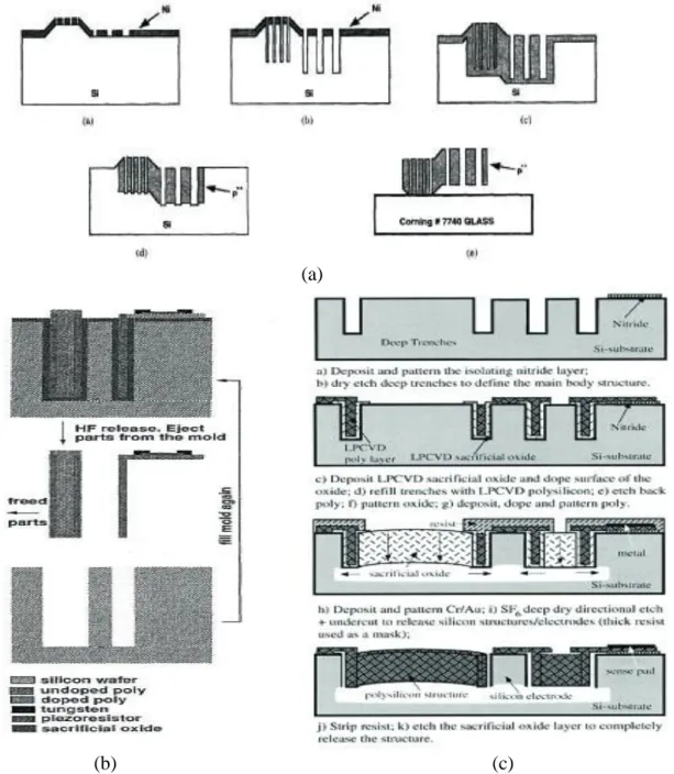
不僅蝕刻速率提升至3~5 μm/min,垂直度 90±1˚,在高速蝕刻機台及參數下,蝕刻速率可高達 20 μm/min, 因無加工圖形限制、蝕刻速率快及垂直度佳,使得目前 ICP-RIE 製程技術,在製作各種高深寬比之單 晶矽微結構上,扮演舉足輕重的角色。雖 ICP-RIE 機台設備不便宜,但隨著蝕刻技術的發展及機台的 普及,蝕刻製程成本也降低到能被接受的範圍,同時,各種單晶矽微機電產品的問市,也反映出 ICP-RIE 此技術值得發展的潛力。 由於單晶矽懸浮結構在微感測器及微致動器的應用廣泛,文獻上,許多製作懸浮結構製程平台技 術,在很早期就被開發出來,以製程特性來分類,大致上可分為三種不同製程類型,如圖 2-1 所示, 分 為 犧 牲 層 型 SOI[23-25] 、 結 構 填 入 型 Deep etching/Shallow diffusion[26] 、 HEXSIL[27] 及 HARPSS[28] ,如圖 2-2 所示,結構保護型 SCREAM[29, 30]、SBM[31]及 BELST[32, 33],如圖 2-3 所
示。
犧牲層型是選用訂製的特殊晶片(Silicon on Insulator, SOI),SOI 晶片為矽-二氧化矽-矽三層結構 所構成,上方為單晶矽結構層,中間為二氧化作為矽絕緣層或犧牲層,底層為單晶矽基板,利用非等 向性離子蝕刻結構層後,再將中間之二氧化矽當作犧牲層蝕刻掉,即可製作出懸浮結構,製程簡便及 快速,但 SOI 晶片費用昂貴,成本考量導致此製程方式無法普及。 結構填入型是利用非等向性離子蝕刻出結構模型後,其中一種製程是利用摻雜硼的方式,摻雜硼 的單晶矽與純單晶矽有蝕刻選擇比的差異,因此,蝕刻純單晶矽而留下不被蝕刻有摻雜硼的單晶矽部 分,以摻雜硼的單晶矽作為懸浮結構,如圖 2-2(a)。另外方法是利用先填入二氧化矽當作犧牲層,再填 入 Poly-silicon 當主要結構,將二氧化矽蝕刻掉而拿出 Poli-Siliocn 主要結構(圖 2-2(b))或直接形成懸 浮結構(圖 2-2(c))。結構填入型的製程步驟繁瑣且複雜。 結構保護型是利用一層保護材料包覆住單晶矽結構,避免懸浮蝕刻製程時,蝕刻到單晶矽結構,
一般以蝕刻選擇比較高之二氧化矽(SiO2)或硼摻雜層(Boron Doping)來當作保護材料,大致來說,
其他搭配的製程材料及製程方式變為複雜。
圖 2-1 懸浮結構製程平台技術 (a)犧牲層型 (b)結構填入型 (c)結構保護型
(a)
(b) (c)
圖 2-2 結構填入型製程技術 (a) Deep etching/shallow diffusion (b) HEXSIL (c) HARPSS (c) (c) (b) (b) (a) (a)
(a)
(b) (c)
彙整上述文獻中所討論製作懸浮結構製程技術的方法,如表 2-1 所示,在非等向性蝕刻上,全是 利用電漿離子蝕刻來達成,可見電漿離子蝕刻的重要性。犧牲層型 SOI 晶片成本太高,結構填入型因 製程太過複雜,而結構保護型使用一般晶片且製程相較簡化,各自有特色。目前,若無成本考量,一 般研究人員仍選擇用 SOI 晶片來製作懸浮結構,其主要原因為製程時程短,可快速驗證設計。因此, 若能有一快速體型微加工製程平台,使用一般晶片製程降低成本,簡化製程機台來縮短製程時程,則 能加速創新的設計實現。 表 2-1 懸浮製程技術比較
3. PoPLSE 製程平台
3.1.
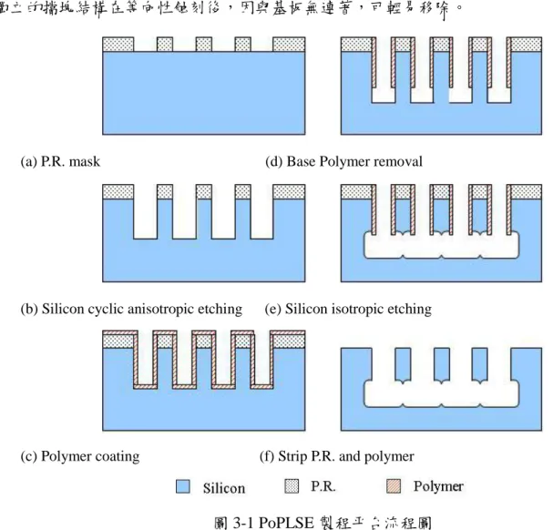
PoPLSE 製程設計與方法以高分子作為蝕刻保護層來製作單晶矽懸浮結構 (Polymer Passivation Layer for Suspended structures Etching,PoPLSE)製程平台技術,是屬於結構保護型的製作方法之一。ICP-RIE 機台中之高 分子材料原是作為非等向性蝕刻用途,並無使用在對等向性蝕刻的保護層。PoPLSE 製程同時以高分子 材料作為非等向性及等向性蝕刻之保護層,除黃光製程外,其餘製程皆整合在 ICP-RIE 機台中完成。 製作懸浮結構最關鍵之製程部分,即是保護層的步驟,標準 ICP-RIE Bosch 製程交替蝕刻中,高分子(CF2) 原是用來當作提高非等向性蝕刻目的之鈍化膜,在非等向性蝕刻後,側壁上雖有一層高分子材料,但 此層高分子保護膜是無法直接抵擋長時間的等向性蝕刻,因此,需要額外的保護膜製程,才能製作出 懸浮結構,因此,相關基本製程參數的研究極為重要。 本論文提出以高分子作為製作懸浮結構之保護層,其中的製程步驟,大致可分為非等向性蝕刻及 等向性蝕刻。因為高分子沈積與去除為電漿離子態的製程方式,加上非等向性蝕刻及等向性蝕刻步驟,
全部製程步驟皆為電漿離子態形式,可說是全電漿製程流程,同時電漿離子製程過程中,雖然離子蝕 刻會有熱反應的產生,但晶片背面有氦氣作為冷卻氣體,可讓製程溫度維持在 45 度之低溫製程。
PoPLSE 製程流程圖,如圖 3-1 所示,此製程選用一般單拋矽晶片< 100 >來製作,首先,進行標準
RCA clean 矽晶片後,旋塗正型光阻(AZ4620) 在矽晶片,黃光微影完成結構圖形當作後續蝕刻的遮罩
及結構上方保護層,如圖 3-1(a),之後的製程步驟則全部在 ICP-RIE 機台製程腔體中進行,如圖 3-1(b) 至圖 3-1(f)。圖 3-1(b)為進行非等向性蝕刻,此蝕刻深度決定懸浮結構之厚度,然後進行等向性高分子 薄膜沈積,將矽結構包覆起來(如圖 3-1(c)),再用非等向性蝕刻將底部高分子薄膜移除,此時可選擇 是否加入氧氣或氬氣於蝕刻氣體中,幫助移除底部高分子薄膜,同時往矽基材下方蝕刻一些深度,此 步驟幫助移除結構底部的矽材能順利進行(如圖 3-1(d));最後,進行等向性蝕刻,利用底切效應移除 矽材結構底部材料,形成懸浮結構(如圖 3-1(e)),即完成懸浮結構製作。若要將光阻及高分子薄膜移 除的話,可以通入氧電漿來去除(圖 3-1(f))。另外,若後續需濺鍍金屬層當驅動電極,未避免矽材導 通,可以重新再沈積一層高分子薄膜當作金屬電極層與矽材間的絕緣層。為避免不同開口尺寸,因蝕 刻延遲及質傳效應導致結構蝕刻深度不同的問題,可於主要結構旁加入獨立的擋塊,使蝕刻的開口一 致,獨立的擋塊結構在等向性蝕刻後,因與基板無連著,可輕易移除。
(a) P.R. mask (d) Base Polymer removal
(b) Silicon cyclic anisotropic etching (e) Silicon isotropic etching
(c) Polymer coating (f) Strip P.R. and polymer
3.2.
ICP-RIE 各基本製程參數之影響ICP-RIE 的參數非常多,影響蝕刻結果的參數有反應氣體的種類、氣體流量及時間、上/下電極的
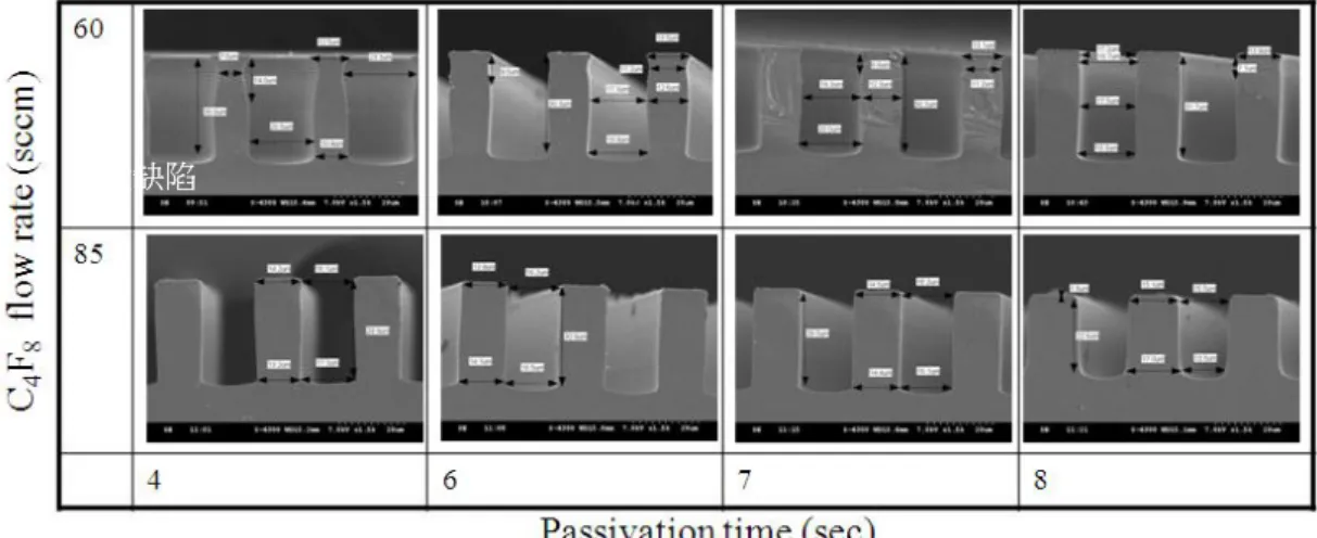
功率、製程腔體的壓力及軟體上的控制,如 overrun time 及 Ramp 功能。上電極:為提供氣體解離的能 量,獲得所需的電漿離子,上電極功率越高氣體解離效率越好,獲得有效的電漿離子濃度越高。下電 極:為提供腔體內一靜電偏壓,使帶電的電漿離子受偏壓吸引,而具有方向性的移動,同時增加物理 性轟擊的效果,下電極功率增加則離子轟擊越強,若不施加下電極,則電漿離子在腔體內以擴散方式 呈等向性的移動。氣體:為蝕刻與保護機制電漿離子的來源,在矽蝕刻中目前以 SF6/C4F8為主要蝕刻 與保護氣體為主。而蝕刻與保護時間:控制每一個蝕刻週期時間,可改變側壁波紋的大小,時間越短 的蝕刻保護週期,可以獲得較佳的側壁粗糙度。Overrun 時間:蝕刻與保護有重疊通入的時間,可緩和 側壁波紋的大小,降低側壁粗糙度。Ramp:以每一週期為單位,隨之增加或減少時間的軟體功能,一 般而言,蝕刻深度越深時,因質傳效果影響,使得結構越深,每一週期蝕刻的深度越淺,Ramp 功能可 依每週期增加一定比例通入的時間,來補償因蝕刻深度變深,導致每一週期蝕刻之深度不同。除了蝕 刻參數的因素外,影響蝕刻品質的因素,還有矽晶片規格、遮罩材料的種類、蝕刻的面積大小及不同 開口的結構,均會導致蝕刻結果的不同,所以也需一併考量。 ICP-RIE 是利用 Bosch 交替蝕刻機制來進行非等向性矽深蝕刻,因此,在蝕刻側壁會產生如波紋 之結構形貌,如圖 3-2(a)所示,側壁波紋為蝕刻保護交替蝕刻下所產生的正常現象,因側壁粗糙度欠佳, 在一些光學元件、單晶矽模仁及高靈敏度感測器上,則無法使用。圖 3-2(b)為不同的開口尺寸下,蝕 刻深度不同之情形,在同一片蝕刻晶片中,不同開口尺寸的結構,因質傳等因素導致蝕刻速率明顯不 同,此稱為活性離子蝕刻延遲現象(Etching Lag)[34,35],可加入補償結構,讓蝕刻開口尺寸一致, 避免蝕刻延遲的現象。圖 3-3(a)則為底部側蝕的 Notch 現象,常發生於 SOI 晶片或穿孔蝕刻製程中, Notch 發生的原因是蝕刻底部為介電材料,導致電荷累積在介電材料的表面上,與電漿離子因同電荷相 斥,反彈至側向矽材料上,時間越久側蝕情形越嚴重[36,37]。圖 3-3(b)則為結構偏上方被蝕刻成碗狀形 狀,其原因為結構偏上方處,承受較多因光阻結構影響行進方向而來之離子攻擊,當蝕刻效果大於保 護效果時,即會產生側壁碗狀形狀[38]。 良好的非等向性蝕刻,需由適當的蝕刻與保護比例才能達成,蝕刻與保護的比例不對,將直接影 響蝕刻的結構垂直度,如圖 3-4 所示,蝕刻效果大於保護的比例,蝕刻結構將形成結構底部外擴的情 形,如圖 3-4 (a),相反地,蝕刻效果小於保護的比例,則結構將形成底部結構內凹的情況,如圖 3-4 (b)。 反應電漿離子濃度不足時,輕微導致蝕刻之粗糙度變差,嚴重時側壁粗糙變糟及結構底部出現雜草的
現象,如圖 3-4(c)。遮罩的選擇也會影響蝕刻,當選用較軟性的材料如光阻時,因光阻邊角較容易被離 子轟擊移除,因此容易產生結構上部側蝕的情況,硬質的遮罩材料如 SiO2及 Si3N4則能降低此現象。 (a) (b) 圖 3-2 (a)側壁波紋結構 (b)因蝕刻延遲效應導致蝕刻深度不一 (a) (b) 圖 3-3 (a) Notch 效應導致蝕刻底部側蝕情形 (b)受光阻結構影響離子行進方向導致之側壁碗狀缺陷 底部側蝕 底部側蝕 碗狀缺陷 碗狀缺陷
(a) (b) (c) 圖 3-4 (a)蝕刻效率大於保護效率,導致蝕刻結構底部形成外擴現象 (b)蝕刻效率小於保護效率,導致蝕 刻結構底部形成內凹情形 (c)蝕刻結構側壁粗糙化及結構底部雜草現象
4. PoPLSE 製程平台:非等向性蝕刻
4.1.
製程壓力及 SF6蝕刻氣體流量之影響 非等向性蝕刻品質受到 ICP -RIE 各參數影響極大,不適當的參數,直接反應在蝕刻結構垂直度及 形貌上,圖 4-1 為製程腔體壓力及蝕刻氣體 SF6流量對蝕刻形貌的影響,圖 4-2 為對應之蝕刻速率。其 他參數為 A)蝕刻步驟:上/下電極 1000/12W,氣體流量 O2 13 sccm,時間 12 sec,B)保護步驟:上/下 電極 1000/0 W,氣體流量 C4F8 85 sccm,時間 8 sec,製程週期 60 cycle。製程腔體中的壓力越低,則 電漿相互碰撞機率降低,基本上可獲得較佳的非等向性蝕刻,但腔體壓力越低,則真空度高,則會減 少電漿濃度,使蝕刻速率變慢。在壓力 15 mTorr 及 SF6流量為 65 sccm 時,電漿離子濃度不足,導致 結構底部出現雜草現象。另 SF6的流量越大,提供可蝕刻矽的氟離子濃度升高,使蝕刻速率提升;但 在製程壓力 15 mTorr、SF6流量 195 sccm 時,因氣體流量太大導致製程無法穩定維持在 15 mTorr 而發 生製程中斷情形。在 SF6流量為 130 sccm,不同製程壓力下,發現蝕刻結構底部形狀,由內凹轉變為 外擴的情形,可知在不同製程壓力下會導致蝕刻與保護比例改變。由圖 4-2 所示,蝕刻速率隨蝕刻氣 外擴 外擴 內凹 內凹 雜草 雜草體 SF6流量及製程壓力增大而增加。 圖 4-1 製程腔體壓力及 SF6蝕刻氣體流量對蝕刻結構形貌的影響 圖 4-2 製程腔體壓力及 SF6蝕刻氣體流量對蝕刻速率之關係圖
4.2.
SF6蝕刻氣體流量及蝕刻時間之影響 蝕刻氣體 SF6流量及蝕刻時間對蝕刻形貌的影響如圖 4-3 所示,圖 4-4 為對應之蝕刻速率。其他 參數為 A)蝕刻步驟:上/下電極 1000/12 W,氣體流量 O2 13 sccm,B)保護步驟:上/下電極 1000/0 W,氣體流量 C4F8 85 sccm,時間 8 sec,製程腔體壓力 35 mTorr,製程週期 60 cycle。SF6流量增大,直接
提供更多的蝕刻氟離子參與反應,因此,蝕刻速率提高,但由圖 4-4 中,SF6流量由 130 sccm 提高到 195 sccm 時,蝕刻速率增加並不多,其原因可能為反應之離子濃度已與蝕刻面積達飽和狀態。另在蝕 刻時間 12 sec,SF 流量從 65 sccm 提高到 195 sccm 可發現,結構形貌由內凹轉變為外擴的現象,即為 1.00 1.50 2.00 2.50 3.00 3.50 4.00 0 100 200 300 SF6 Flow (sccm) E tc h ra te ( μ m /m in ) Chamber pressure 15mTorr Chamber pressure 25mTorr Chamber pressure 35mTorr 雜草 雜草 外擴 外擴 內凹 內凹
蝕刻與保護的比例改變所致。 圖 4-3 SF6蝕刻氣體流量及蝕刻時間對蝕刻結構形貌的影響 圖 4-4 SF6蝕刻氣體流量及蝕刻時間對蝕刻速率之關係圖
4.3.
C4F8保護氣體流量及保護時間之影響 圖 4-5 為不同流量保護氣體 C4F8及保護時間對蝕刻形貌的影響,圖 4-6 為對應之蝕刻速率。其他 參數為 A)蝕刻步驟:上/下電極 1000/12 W,氣體流量 SF6/O2 130/13 sccm,時間 12 sec,B)保護步驟: 上/下電極 1000/0 W,製程腔體壓力 35 mTorr,製程週期 60 cycle。通入的保護氣體 C4F8流量及時間增 加下,底部鈍化膜增厚,需移除底部鈍化膜的時間增加,而降低了蝕刻速率。在保護氣體 C4F8流量 85 sccm,保護時間由 4 sec 增加至 8 sec,明顯發現結構底部由外擴轉變為內凹情形,可見保護時間影響 蝕刻結果極為敏感。另外保護氣體 C4F8流量 60 sccm 時發現,結構偏上方形成碗狀的蝕刻缺陷,造成 此原因為保護膜厚度不足,加上結構偏上方遭受到較多因光阻而改變行進方向的離子攻擊所導致[38], 需增加保護時間來提高保護膜厚度解決。 0.00 0.50 1.00 1.50 2.00 2.50 3.00 3.50 8 12 16 20 Etch time (sec)E tc h ra te ( μ m /m in ) SF6 flow65sccm SF6 flow 130sccm SF6 flow 195sccm
圖 4-5 C4F8保護氣體流量及保護時間對蝕刻結構形貌的影響 圖 4-6 C4F8保護氣體流量及保護時間對蝕刻速率之關係圖
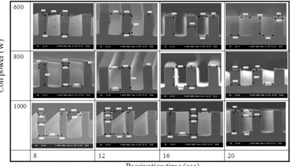
4.4.
上電極功率及保護時間之影響 圖 4-7 為上電極功率及保護時間對蝕刻形貌的影響,圖 4-8 為對應之蝕刻速率。其他參數為 A)蝕 刻步驟:下電極 12W,氣體流量 SF6/O2 130/13sccm,時間 12sec,B)保護步驟:下電極 0W,氣體流量 C4F8 85 sccm,製程腔體壓力 35mTorr,製程週期 60 cycle。上電極為提供氣體解離能量,上電極功率 越大,所解離出的離子濃度越高,在保護時間 8sec,上電極由 600W 提高到 1000W,發現結構偏上方 出現側壁碗狀缺陷,同時蝕刻深度增加,表示,同樣參數條件下,上電極功率增大,對於蝕刻效果的 影響大於保護效果。 1.00 1.50 2.00 2.50 3.00 3.50 2 4 6 8 10Passivation Time (Sec)
E tc h Ra te ( μ m /m in ) C4F8 flow 72sccm C4F8 flow 85sccm 碗狀缺陷 碗狀缺陷
圖 4-7 上電極功率及保護時間對蝕刻結構形貌的影響 圖 4-8 上電極功率及保護時間對蝕刻速率之關係圖
4.5.
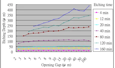
高深寬比蝕刻 高深寬比結構蝕刻除了需要蝕刻較深的結構深度外,保持結構的垂直度及確保結構幾何尺寸也相 當重要,且整體製作的蝕刻速率也是外一項重要的考量因素,蝕刻速率太慢,則會影響蝕刻時間過長, 產量過低而失去其意義。因此,提高蝕刻反應,調高蝕刻氣體流量及時間、上電極及下電極電壓,最 後再調整適當相對之保護反應比例,獲得垂直度佳之蝕刻效果。 基於前述所建立的參數影響趨勢,調整出最佳化之蝕刻製程參數,獲得最佳之矽非等向性蝕刻參數 為 A)蝕刻步驟:上/下電極 800/12 W,氣體流量 SF6/O2 130/13 sccm,時間 12 sec,B)保護步驟:上/下 電極 800/0 W,氣體流量 C4F8 85 sccm,時間 8 sec,製程腔體壓力 35 mTorr,蝕刻速率在結構線寬 10 μm 處為2.3 μm/min。以此參數蝕刻出之溝槽結構。如圖 4-9(a)所示,為結構線寬/開口尺寸 2 μm 的溝槽結 構,蝕刻深度約60 μm,深寬比為 30,垂直度 89±1°。圖 4-9(b)為結構線寬/開口尺寸 5 μm 的溝槽結構, 蝕刻深度約68 μm,深寬比為 15,垂直度為 89±1°。 1.00 1.50 2.00 2.50 3.00 3.50 2 4 6 8 10Passivation Time (Sec)
E tc h Ra te ( μ m /m in ) Coil power 600W Coil power 800W Coil power 1000W
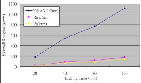
(a) (b) 圖 4-9 良好垂直度之非等向性蝕刻 (a)結構線寬/開口 2 μm 的溝槽結構,蝕刻深度約 60 μm,深寬比為 30 (b)結構線寬/開口 5 μm 的溝槽結構,蝕刻深度約 68 μm 以開發出之最佳高深寬比蝕刻參數進行蝕刻,並建立相對應之各項規格,圖 4-10 為溝槽結構線寬 /開口尺寸為 2, 3, 4, 5, 6, 7, 8, 9, 10, 15, 20, 30, 40, 50 及 100 μm,蝕刻時間與蝕刻深度的關係,蝕刻深 度越深時,因不同尺寸質傳效果不同的關係,導致蝕刻深度不一致,這即是蝕刻延遲的現象,在蝕刻 20 min 後,結構線寬/開口尺寸 2 μm 與 100 μm,蝕刻深度差異為 9 μm,在蝕刻 40 min 後,結構線寬/ 開口尺寸2 μm 與 100 μm,蝕刻深度差異增為 25 μm,在蝕刻 160 min 後,結構線寬/開口尺寸 5 μm 以 下的結構已不見,而結構線寬/開口尺寸 5 μm 與 100 μm,蝕刻深度差異高達為 195 μm,可見小線寬的 尺寸,在蝕刻深度加深後,質傳效果遽增,導致蝕刻深度下降,蝕刻速率明顯降低。圖 4-11 為蝕刻時 間與側蝕情形的關係圖,在蝕刻 40 min,側蝕小於 1.5 μm,而蝕刻 160 min 後,側蝕小於 3 μm。圖 4-12 為蝕刻時間與垂直度之關係圖,蝕刻 40 min ,垂直度為 89±1˚,在蝕刻 160 min ,垂直度為 87±1˚。 在蝕刻側壁粗糙度上,以 AFM 進行量測,量測方式為取蝕刻深度之中間部份 10 μm×10 μm 範圍,結 構線寬10 μm 下,蝕刻時間與側壁粗糙度之關係圖,如圖 4-13 所示,蝕刻 20 min,側壁粗糙度為
18 nm(Ra),蝕刻 40 min,側壁粗糙度為 73 nm(Ra),蝕刻 160 min,側壁粗糙度為 145 nm(Ra),蝕刻越
圖 4-10 不同蝕刻開口尺寸,蝕刻時間與蝕刻深度的關係圖 圖 4-11 不同開口尺寸下,蝕刻時間與側蝕關係圖 圖 4-12 不同開口尺寸下,蝕刻時間與垂直度關係圖 Etching time 0 50 100 150 200 250 300 350 400 450 2 3 4 5 6 7 8 9 10 15 20 30 40 50 100 Opening Gap (μ m) E tc hin g D ep th ( μ m) 4 min 12 min 20 min 40 min 80 min 120 min 160 min Opening Gap 0.00 0.50 1.00 1.50 2.00 2.50 3.00 3.50 4 12 20 40 80 120 160
Etching time (min)
S id e E tc hi ng a t to p po si ti on (μ m) 2μ m 4μ m 6μ m 8μ m 10μ m
圖 4-13 側壁粗糙度與蝕刻時間之關係圖
5. PoPLSE 製程平台:等向性蝕刻
5.1.
高分子沈積及底部高分子去除 在 Bosch 專利蝕刻機制中,高分子是由 C4F8氣體解離成電漿離子,進而沈積成高分子薄膜,電漿 離子是由 CFx+、CFx*和 F*等化合物組成, CFx*化合物經 由吸附作用,在矽結構表面形成高分子薄膜, 藉由這層 CF2薄膜來阻擋氟離子蝕刻矽質材料。高分子材料經由 Hitachi S-4300 場發射掃瞄電子顯微 鏡中 EDS,進行高分子薄膜成分分析,如圖 5-1 所示,高分子成份由 45%的碳及 55%的氟組成。待測 之高分子為厚度 500 nm 沈積於矽基板上,高分子沈積參數為上/下電極 800/0W,C4F8氣體流量 130 sccm, 製程腔體壓力 35 mTorr,時間 5 min,EDS 之加速電壓為 15 kv,1x10-5 Pa 真空度。 圖 5-1 高分子薄膜 EDS 成分分析 在 Bosch 蝕刻保護交替機制來獲得高深寬比蝕刻中,產生的側壁波紋結構會影響高分子沈積覆蓋 的結果,波紋結構會對高分子進行沈積時,產生遮蔽的影響,使得在波紋結構下方,高分子薄膜不容 0 200 400 600 800 1000 1200 20 40 80 160Etching Time (min)
Si de w al l Ro ug hn es s (n m ) Z-RANGE(nm) Rms (nm) Ra (nm)
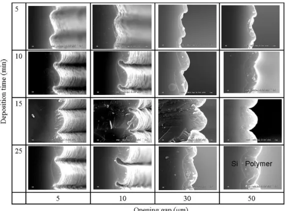
易覆蓋好,在等向性蝕刻時,容易對高分子覆蓋有缺陷的地方,產生矽結構蝕刻現象,因此,對於高 分子在側壁波紋結構及不同開口尺寸下的覆蓋效果,先進行研究。 利用 Bosch 非等向性標準高深寬比蝕刻參數,蝕刻出深度 30 μm 的溝槽結構,溝槽開口尺寸分別 為 5、10、30 及 50 μm,高分子沈積時間 5, 10, 15 及 25 min,來探討高分子沈積及底部高分子移除的 情形。 在高分子沈積過程中,不提供下電極靜電偏壓,讓高分子利用擴散方式,等向性的覆蓋在矽結構 的表面,在不同開口尺寸及沈積時間下,高分子薄膜沈積在溝槽結構側壁之 SEM,所圖 5-2 所示,高 分子薄膜沈積在溝槽結構底部之 SEM,所圖 5-3 所示。 在不同沈積條件下,以 SEM 量測高分子沈積在結構表面的厚度,如圖 5-4 所示,高分子是用來作 為製作懸浮結構製程中,抵擋等向性蝕刻之保護矽結構材料,必頇確保矽結構的側壁完全被高分子包 覆,因此,側壁所沈積的高分子厚度,量測其最小值,圖 5-4(a)為高分子沈積在矽結構側壁量測之最小 厚度值,最小厚度發現在結構偏下方處,因質傳效果影響所致。在相同高分子沈積時間下,沈積在開 口尺寸小的高分子薄膜的厚度小於沈積在開口尺寸大的。在開口尺寸5 μm 及 10 μm 處,由於側壁波紋 結構的遮蔽效果,導致波紋結構下方沈積較薄的高分子薄膜,加上沈積時間短如 5 min 時,發現在某 些波紋結構下方,沒有高分子薄膜沈積,厚度量測值為 0,將高分子沈積時間由 5 min 增加至 25 min 來增加沈積的高分子薄膜厚度,在波紋結構下方的高分子薄膜厚度,依然遠薄於沈積在其他結構的區 域。為改善在開口尺寸小,因波紋結構遮蔽效應導致高分子薄膜沈積覆蓋性差的問題,可以調整非等 向性蝕刻的參數,降低側壁波紋結構及粗糙度,如本論文 3.2.2 節所述,側壁鏡面蝕刻可有效改善因波 紋導致高分子覆蓋差的情形。在開口尺寸30 μm 及 50 μm 時,側壁波紋結構之遮蔽效果影響變小,高 分子薄膜能較均勻地沈積在側壁表面。 由於在製作懸浮結構製程中,底部高分子薄膜需要完全去除,以利後續的等向性蝕刻的進行,因 此,沈積在結構底部高分子薄膜厚度,量測其最大值,如圖 5-4(b)所示,沈積在結構底部高分子薄膜 的厚度,隨著開口尺寸及沈積時間的增加而增厚。底部高分子薄膜移除之非等向性蝕刻參數為上/下電 極 800/12 W,氣體 SF6/O2 130/13 sccm,製程腔體壓力 35 mTorr,在溝槽結構深度 30 μm 及四種不同開 口尺寸下,因質傳效果,開口尺寸較大處有較高的高分子薄膜移除速率,如圖 5-5 所示。
圖 5-2 高分子薄膜沈積在溝槽結構側壁之 SEM 圖,溝槽結構深度為 30 μm,開口尺寸為 5、10、30、 50 μm 及高分子沈積時間 5、10、15、25 分鐘
圖 5-3 高分子薄膜沈積在溝槽底部之 SEM 圖,溝槽結構深度為 30 μm,開口尺寸為 5、10、30、50 μm 及高分子沈積時間 5、10、15、25 分鐘
(a) (b) 圖 5-4 在不同開口尺寸及沈積時間下,溝槽結構 30 μm 之高分子薄膜厚度量測 (a) 側壁高分子量測厚 度最小值 (b)結構底部高分子量測厚度最大值 圖 5-5 不同開口尺寸下,結構 30 μm 底部高分子移除速率
5.2. 結構深度 30 μm 之等向性蝕刻
利用等向性蝕刻將懸浮結構底部之矽材料移除,及等向性蝕刻之側蝕情形、蝕刻速率與結構開口 尺寸及結構深度有關,本實驗預先蝕刻出結構深度30μm 開口尺寸分別為 5μm、10μm、30μm、50 μm 後,進行高分子保護層之沉積後再使用非等向性蝕刻轟擊將結構底部所沉積之高分子保護層去除只留 下側壁高分子保護層後開始等向性蝕刻,等向性蝕刻後發現底部未受高分子保護層之矽基材越靠近原 始結構底部之位置開口越大,因等向性蝕刻呈現出碗狀形狀,因離子往每個方向蝕刻之機率較相同所 致,離子反應未受阻,蝕刻速率較快,開口尺寸越小及結構深度越深時,受限於光阻及矽結構影響, 蝕刻離子需行經光阻結構及矽結構深度,才能到達底部矽表面產生蝕刻反應,如圖 5-6 所示,因此蝕 刻速率下降,同時蝕刻形狀並非呈碗狀,而呈現似菱形的蝕刻形狀,開口尺寸越小,側蝕蝕刻速率越 慢,蝕刻形狀越趨菱形,其參數為高分子沈積時間為 10 分鐘,底部高分子移除時間為 8 分鐘及等向性 蝕刻時間為 6 分鐘。(a) (b) (c) (d) 圖 5-6 結構深度 30 μm,不同開口尺寸(a)5 (b)10 (c)30 (d)50 μm 之等向性蝕刻結果
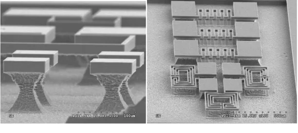
5.3. 懸浮結構製程結果
基於優化的參數研究,於結構厚度30 μm 及結構線寬/開口尺寸 5 μm 之單晶矽懸浮結構,在高分 子沈積時間為 10 分鐘、底部高分子去除時間為 8 分鐘及等向性蝕刻時間為 6 分鐘的參數下,可以成功 製作出來。因為 PoPLSE 製程平台製作懸浮結構在同一片單晶矽晶片上,除懸浮結構處外,需有支撐 結構處,因此支撐結構處的尺寸需大於懸浮結構處,如圖 5-7 所示,利用尺寸的差異性,控制好懸浮 蝕刻的時間,來決定懸浮的結構。圖 5-8(a)為利用 PoPLSE 製程平台技術製作之結構深度 30 μm,結構 線寬5 μm 之梳狀致動器,圖 5-8(b)為側向放大圖,可明顯看出懸浮微結構側壁被保護而底部懸浮掏空 的結果。各種微感測器如微陀螺儀、微電容感測器、扭轉式梳狀致動器及微鑷子致動器等,都能利用 所提出之 PoPLSE 製程平台製程技術製作,如圖 5-9。(a) (b)
圖 5-7 利用線寬尺寸的差異,懸浮與未懸浮的結構
(a) (b)
(a) (b) (c) (d) 圖 5-9 PoPLSE 製程平台技術製作出各式厚度 30 μm 之微結構 (a)微陀螺儀 (b)微電容感測器 (c)扭轉式 梳狀致動器 (d)微鑷子致動器 懸浮結構結構線寬增加時,除等向性蝕刻時間隨之增加,其高分子沈積及底部高分子移除的參數 也需隨之調整。以結構深度30 μm、結構寬度 10 μm 之梳狀結構來討論適合的參數,圖 5-10(a)為高分 子沈積時間 10 分鐘、底部高分子移除時間 8 分鐘,等向行蝕刻時間 9 分鐘,所製作之懸浮梳狀結構。 靠近結構下方依然有因高分子沒保護好微結構,而導致被蝕刻的結構缺陷。增加高分子沈積時間到 15 分鐘、底部高分子移除時間隨之調整至 10 分鐘,等向性蝕刻時間維持 9 分鐘,可以成功製作出結構寬 度10 μm、結構深度 30 μm 之懸浮梳狀結構,如圖 5-10(b)所示。 當結構深度增加,結構越深高分子越不容易沈積,因此沈積時間得增長,同時底部高分子移除及 等向性蝕刻參數也需隨之調整。圖 5-11 為利用 PoPLSE 製程平台技術,成功製作結構深度 60 μm,結 構寬度各為5 μm 及 10 μm 之梳狀懸浮微結構,製程參數為高分子沈積時間 25 分鐘,底部高分子移除 時間 14 分鐘及等向性蝕刻時間 9 分鐘。
(a) (b) 圖 5-10 結構線寬/開口尺寸 10 μm、結構深度 30 μm 之懸浮梳狀結構 (a)因不足的高分子保護導致結構 缺陷(高分子沈積 10 分鐘、底部高分子移除 8 分鐘及等向性蝕刻 9 分鐘) (b)成功製作之梳狀結構 (高 分子沈積 15 分鐘、底部高分子移除 10 分鐘及等向性蝕刻 9 分鐘) (a) (b) 圖 5-11 成功製作之梳狀結構,結構深度 60 μm,結構線寬/開口尺寸 (a)5 μm (b) 10 μm
6. 結論
PoPLSE 製程之各項參數對於元件製作皆有相當大的影響,進行非等向性蝕刻主要以製程壓力、SF6 蝕刻氣體流量、蝕刻時間、C4F8保護氣體流量、保護時間及上電極功率為主要影響因素,而針對各參 數進行優化進而得到高深寬比、結構垂直性佳及較佳的側壁粗糙度。於等向性蝕刻製程中主要影響參 數為高分子沉積時間、高分子層去除時間及等向性蝕刻時間,本研究以深度30 μm 之溝槽結構於開口 尺寸 5、10、30 及 50 μm 進行測試,觀察側壁高分子沈積及底部高分子去除於不同開口尺寸下之趨勢。 並探討在不同結構線寬、開口尺寸及結構深度等條件下,底部高分子移除及等向性懸浮對高分子保護 膜之影響,並且得到優化參數成功釋放梳狀結構以驗證 PoPLSE 製程平台製作懸浮結構可行性。PoPLSE 製程平台技術利用高分子作為蝕刻保護層來製作懸浮結構,可簡化製程機台、縮短製程時間、降低製 程晶片成本及應用共通性廣等為此 PoPLSE 製程平台的優勢。7. 參考資料
[1] K. E. Peterson, Silicon as a mechanical material, Proc. IEEE, vol.70, no. 5, pp. 420-457, 1982
[2] http://www.jahm.com/:Temperature Dependent Elastic & Thermal Properties Database
[3] G. T. A. Kovacs, N. I. Maluf and K. E. Petersen, Bulk micromachining of silicon, Proc. IEEE, vol. 86, no. 8, 1998
[4] H. R. Robbins and B. Schwartz, Chemical etching of silicon-I. The system HF, HNO3 H2O and HC2C3O2,
Journal of The Electrochemical Society, vol. 106, no. 6, pp. 505–508, 1959
[5] H. R. Robbins and B. Schwartz, Chemical etching of silicon-II. The system HF,HNO3 H2O and HC2C3O2,
Journal of The Electrochemical Society, vol. 107, no. 2, pp. 108–111, 1960
[6] B. Schwartz and H. R. Robbins, Chemical etching of silicon-III. A temperature study in the acid system,
Journal of The Electrochemical Society, vol. 108, no. 4, pp. 365–372, 1961
[7] J. B. Price, Anisotropic etching of silicon with KOH-H2O isopropyl alcohol, in Semiconductor Silicon, H.
R. Huff and R. R. Burgess, Eds. Princeton, NJ: Electrochemical Society, pp. 339-353, 1973
[8] B. Schwartz and H. R. Robbins, Chemical etching of silicon-IV. Etching technology, Journal of The Electrochemical Society, vol. 123, no. 12, pp. 1903–1909, 1976
[9] E. Bassous, Fabrication of novel three-dimensional microstructures by the anisotropic etching of (100) and (110) silicon, IEEE Trans. Electron Devices, vol. ED-25, pp. 1178–1185, 1978
[10] H. Seidel, L. Csepregi, A. Heuberger and H. Baumgartel, Anisotropic etching of crystalline silicon in alkaline solutions I: Orientation dependence and behavior of passivation layers, Journal of The Electrochemical Society, vol.137, no.11, pp. 3612–3626, 1990
[11] H. Seidel, L. Csepregi, A. Heuberger and H. Baumgartel, Anisotropic etching of crystalline silicon in alkaline solutions II: Influence of dopants, Journal of The Electrochemical Society, vol. 137, no. 11, pp. 3626–3632, 1990
[12] F. S. S. Chien, C. L. Wu, Y. C. Chou, T. T. Chen, S. Gwo and W. F. Hsieh, Nanomachining of
110-oriented silicon by scanning probe lithography and anisotropic wet etching, Applied Physics Letters,
vol. 75, no. 16, pp. 2429-2431, 1999
[13] X. Li and P. W. Bohn, Metal-assisted chemical etching in HF/H2O2 produces porous silicon, Applied
Physics Letters, vol. 77, no. 16, pp. 2572-2574, 2000
[14] T. Hadjersi, N. Gabouze, N. Yamamoto, C. Benazzouz, H. Cheraga, Blue luminescence from porous layers produced by metal-assisted chemical etching on low-doped silicon, Vacuum, vol. 80, pp. 366–370, 2005
[15] K. Peng, J. Hu, Y. Yan, Y. Wu, H. Fang, Y. Xu, S. Lee and J. Zhu, Fabrication of single-crystalline silicon nanowires by scratching a silicon surface with catalytic metal particles, Advanced Functional Materials, vol. 16, pp. 387–394, 2006
[16] C. Chartier, S. Bastide and C. L. Clement, Metal-assisted chemical etching of silicon in HF-H2O2,
Electrochimica Acta, vol. 53, pp. 5509–5516, 2008
[17] F. Chamran, Y. Yeh, B. Dunn and C. J. Kim, 3-Dimensional electrodes for microbatteries, ASME Conf.
Proc., IMECE2004-61925, pp. 289-292, 2004
[18] L. M. Ephrath, Reactive Ion Etching, US Patent 4283249, 1979
[19] S. A. McAuley, H. Ashraf, L. Atabo, A. Chambers, S. Hall, J. Hopkins and G. Nicholls, Silicon
micromachining using a high-density plasma source, Journal of Physics D: Applied Physics., vol. 34, pp.
2769–2774, 2001
[20] F. Larmer and A. Schilp, Method of anisotropically etching silicon, US patent 5501893, 1996
[21] A. M. Hynes, H. Ashraf, J. K. Bhardwaj, J. Hopkins, I. Johnsto and J. N. Shepherd, Recent advantages in
silicon etching for MEMS using the ASETM process, Sensors and Actuators A, vol. 74, pp. 13-17, 1999
[22] F. Laermer, A. Schilp, K. Funk and M. Offenberg, Bosch deep silicon etching: improving uniformity and
etch rate for advanced mems applications, Proc. IEEE, pp. 211-216, 1999
[23] J. B. Lasky, Wafer bonding for silicon‐on‐insulator technologies, Applied Physics Letters, vol. 48, pp.
78-80, 1986
[24] M. Bruel, Silicon on insulator material technology, Electronics Letters, vol. 31, no.14, pp. 1201-1202,
1995
[25] S. C. Arney and N. C. MacDonald, Formation of submicron silicon on insulator structures by lateral
oxidation of substrate-silicon islands, Journal of Vacuum Science & Technology B
,
vol. 6, pp. 341-345,1998
[26] W. H. Juan and S. W. Pang, Released Si microstructures fabricated by deep etching and shallow diffusion,
Journal of Microelectromechanical Systems, vol. 5, pp. 18-23, 1996
[27] C. G. Keller and R. T. Howe, HEXSIL tweezers for teleoperated micro-assembly, Proc. IEEE, pp.
72-77, 1997
[28] F. Ayazi and K. Najafi, High aspect-ratio combined poly and single crystal silicon (HARPSS) MEMS
technology, Journal of Microelectromechanical Systems, vol. 9, pp. 288-294, 2000
[29] K. A. Shaw, Z. L. Zhang and N. C. MacDonald, SCREAM I: A Single Mask,
Single-Crystal Silicon, Reactive Ion Etching Process for MicroElectroMechanical
[30] N. C. MacDonaid, SCREAM microelectromechanical systems, Microelectronic Engineering, vol. 32, pp.
49-73, 1996
[31] S. Lee; S. Park, J. Kim, S. Lee and D. Cho, Surface/bulk micromachined single-crystalline-silicon
micro-gyroscope, Journal of Microelectromechanical Systems, vol. 9, pp. 557-567, 2000
[32] J. Hsieh and W. Fang, A boron etch stop assisted lateral silicon etching process for improved high aspect
ratio silicon micromachining and its applications, Journal of Micromechanics and Microengineering,
vol.12, pp. 574-581, 2002
[33] J. M. L. Tsai, H. Y. Chu, J. Hsieh and W. Fang, The BELST II process for silicon HARM vertical comb
actuator and its applications, Journal of Micromechanics and Microengineering, vol. 14, pp. 235-241,
2004
[34] H. Jansen, M. de Boer, R. Wiegerink, N. Tas, E. Smulders, C. Neagu and M. Elwenspoek, RIE lag in
high aspect ratio trench etching of silicon, Microelectronic Engineering, vol. 35, Issues 1–4, pp. 45–50,
1997
[35] S. L. Lai, D. Johnson and R. Westerman, Aspect ratio dependent etching lag reduction in deep silicon
etch processes, Journal of Vacuum Science & Technology A, vol. 24, no. 4, pp. 1283-1288, 2006
[36] J. Li, Q. X. Zhang, A. Q. Liu, W. L. Goh and J. Ahn, Technique for preventing stiction and notching
effect on silicon-on-insulator microstructure, Journal of Vacuum Science & Technology B, vol. 21, pp.
2530-2539, 2003
[37] S. Park, D. Kwak, H. Ko, T. Song and D. Cho, Selective silicon-on-insulator (SOI) implant: a new
micromachining method without footing and residual stress, Journal of Micromechanics and
Microengineering, vol. 15, pp. 1607–1613, 2005
[38] G. Marcos, A. Rhallabi and P. Ranson, Monte Carlo simulation method for etching of deep trenches in Si
國科會補助專題研究計畫出席國際學術會議心得報告
日期:101 年 07 月 31 日
一、參加會議經過
IEEE NEMS Conference 是一有關微工程技術交流之國際研討會,其領域包括生醫感測器、半導體 製程及最新的生物領域相關技術,每年度於世界各地舉辦一次,與會人士皆為世界各地之頂尖學者及 研究人員;今年會議日期為 2012/3/5 至 2012/3/8 共四天,主辦單位為京都大學,會議則於日本的京都 舉行,京都有悠久歷史為日本獲選世界遺產的城市之一,其建築群主要效仿隋唐長安城與洛陽城設計 古稱平安京,於桓武天皇時期完成(西元 794 年)定為國都直到明治天皇(西元 1868 年)遷都東京為止, 為日本歷經千年的政治及文化的中心。 第一天主要於京都大學內辦理報到相關事宜,參加者領取名牌及會議相關資料。第二天至第四天 則為正式議程,包含每日九點開始的例行的研討會議,每日會議歷程分上午與下午共有四個場次,此 外除每日例行研討會議也於午後時段舉行海報報告,讓與會者皆能找到感興趣之研究主題,此次會議 共計有 230 場的口頭報告與 104 場的海報報告。
本實驗室在此會議共發表兩篇論文,其中”Development of Microbead-based Affinity Biosensor by Insulator-Based Dielectrophoresis”是安排為口頭報告論文,於會議的第三天下午,由本實驗室研究生卓
計畫編號
NSC 100-2221-E-009-034-
計畫名稱
以高分子作為感應偶合電漿反應離子蝕刻側壁保護以製作單
晶矽懸浮微結構之快速製程平台研發
出國人員
姓名
徐文祥、卓琮閔
服務機構
及職稱
交通大學機械系教授、研究生
會議時間
2012 年 03 月 05 日 至 2012 年 03 月 08 日會議地點
日本,京都
會議名稱
(中文)奈米/微米工程與分子系統國際研討會
(英文)2012 7th IEEE International Conference on Nano/Micro Engineered
and Molecular Systems
發表題目
共兩篇
Development of Microbead-based Affinity Biosensor by
Insulator-Based Dielectrophoresis
Fabrication of Deep Lateral Single-Crystal-Silicon Blaze Micro-grating by
Inductively-Coupled-Plasma Reactive Ion Etch
並向負責報告的研究生討論研究相關內容,而能透過國際研討會與相關研究領域的學者交談,也讓學
生獲益良多。另一篇”Fabrication of Deep Lateral Single-Crystal-Silicon Blaze Micro-grating by
Inductively-Coupled-Plasma Reactive Ion Etch”,則是安排為壁報論文,也在壁報展示時間同與會學者交 流,獲得寶貴經驗。 而於第三天的晚上所舉辦的餐會,除了可讓與會者放鬆心情外,並可得到更進一步交流的機會, 本實驗室也於晚上餐會中,與結識的數位學者交流有關研究上的各種心得;另外主辦單位也在餐會中, 向與會者宣傳下一屆研討會的資訊,包括會議的日期、地點以及當地特色,期許眾人能於下屆研討會 中,交流更多的研究成果。
二、與會心得
此次研討會中,本實驗室研究生以英文向國際學者報告研究成果,報告情形如圖一所示。另外雖 然受限於時間,無法對研究內容作更進一步的詳細介紹,但對相關領域感興趣之學者,也於報告時間 之後做進一步的交流討論,如圖二所示。 分享研究成果的過程實在令人感到相當興奮,是一種自我實現的成就感,而透過學術交流世界接 軌的過程更是難能可貴。在研討會中各個會議報告都是其精心研究的成果,而利用此次國際交流的機 會,吸收這次研討會所提出的嶄新想法,勢必會對學生日後的研究產生很大的影響力。 此外於一些生醫感測器、生醫化學、半導體製程技術等領域上的收穫也頗豐碩,直到最後一天時 仍有意猶未盡之感,希望時間能持需停留於此刻。此次參加研討會外參訪的當地人文風情、增進了學 術與人文的素養,然而最有趣也最有意義的是進行了許多國民外交,無論是一同前往的教授們、國外 學者、對岸朋友或是台灣學生。 圖一、本實驗室研究生於會場內進行報告之照片圖二、報告結束時與學者討論之照片
在會場也遇到多位台灣教授,一同參與此研討會,如圖三所示,左邊第一位是本人(徐文祥),右邊 第二位是交大電子系鄭裕庭教授,透過討論聽講心得,得到更豐富的經驗分享。
圖三、參加會議之學者合照
三、建議
參加研討會不僅僅是學習,更可以開拓視野深度,探訪當地的風土及其民族精神,這完全取決於 心態,唯有將自我放空與縮小,才能吸收更多養分回國深究。在國內告訴研究生該做哪些準備,學生 常不能體會原因,透過親身經歷,學生更能體會為何要在出國前,事先將所有口頭報告與海報報告的 標題進行了解,挑出有興趣的題目後,到了會場便可快速地進入狀況,迅速地拜訪每個學者,這跟平 常在實驗室閱讀文獻有很大的不同,透過當面的問與答可以加速資訊的吸收之外,更可獲取一些文獻 中沒有包含到的資訊,對於研究工作相當有幫助;此外也可同時留意國內一同與會的學者,即使研究 領域不同,但也可以於會場中結識而替未來的合作留下一個種子。四、攜回資料名稱及內容
研討會紀念提袋,內含: (1)議程簡章 (2)會議手冊(內含報告主題與摘要) (3)光碟(內含論文電子檔) (4)當地交通資訊五、發表論文全文或摘要
本實驗室在此次國際研討會議發表的論文共兩篇,謹附於後。Development of Microbead-based Affinity Biosensor by
Insulator-Based Dielectrophoresis
Tsung-Min Chuo1, Wensyang Hsu1, Shih-Kang Fan1,2
1
Department of Mechanical Engineering, National Chiao Tung University, TAIWAN
2
Department of Materials Science and Engineering, National Chiao Tung University, TAIWAN [email protected]
Abstract—This research describes a high sensitivity
microfluidic bead-based immunosensor based on the principle of insulator-based dielectrophoresis (iDEP). An insulator film with small holes between two electrodes creates a nonuniform electric field. By applying appropriate voltage and frequency, the fluorescent beads are concentrated to lower electric field regions due to the difference of dielectric properties. This concentrating step enhances the fluorescence intensity of analytes and decreases the detection limit of immunosenser. In this research, the fluorescence dye is conjugated with streptavidin which has high affinity to biotin. We use biotin-labeled polystyrene beads to bind with streptavidin, therefore, we can further detect fluorescent streptavidin
conjugates by a fluorescence microscope. The
biotin-labeled polystyrene beads perform not only various chemical characteristics by labeling different functional groups but also offer an increased surface area for antibodies or antigens to immobilize on. Finally, we fabricate a microfluidic bead-based immunosensor with high sensitivity (1 pg/ml), short analysis time (~10 minutes), few sample consumption (~0.5 μl) and without physical microchannel.
Keywords-component; immunosensor; iDEP; fluorescence
1. Introduction
Immunoassays are biochemical analysis methods based on the high selectivity between antibody and antigen; they normally measure the presence or concentration of a specific substance in solutions or mediums that frequently contain a complex mixture of substances. Moreover, immunoassays are among the most sensitive and specific analytical methods that are routinely used in a clinical laboratory and other biological research applications.
In recent years, a new technique that uses microbeads as a solid support in immunoassays has become usual. There are several advantages in the use of microbeads. First, the microbeads’ surface to volume ratio is greater than that of a microtiter plate commonly used in conventional immunoassays. For example, 1 g of microbeads with a diameter of 0.1μm has a total surface area of about 60 m2 [1]. The large surface area provides a large interface and the reaction field between samples and reagents. The sensitivity of immunoassays would be increased as a result of the higher efficiency of the immunoreactions between the immobilized antibody and the antigen present in a continuous flow. In addition, the reaction
Second, the immunoassays which use microbeads as a solid support can be easily integrated into a microfluidic chip. The samples and reagents that used in immunoassays can be easily transported in a fluidic system by a syringe pump or another way. Third, there are various available surface modifications for microbeads. DNA, RNA, antibodies, antigens and a vast number of other biological molecules can be easily fixed on the surface of microbeads. Moreover, transportation and analysis in a fluidic system is easy [2].
Furthermore, the dynamic condition that utilizing both diffusion and convectional forces to deliver or mix samples with reagents in microfluidic system. In contrast, conventional immunoassay on a microtiter plate, likes enzyme-linked immunosorbent assay (ELISA), is a static condition that merely depends on diffusion of the molecules for interaction and binding.
Microfluidic technology is widely used in immunoassays available to improve the analytical characteristic performances, such as short analysis time, high reliability and high detecting sensitivity, easy handling and low consumption of reagents [3]. However, a retention method is necessary for trapping or fixing microbeads in microfluidic system in order to avoid the microbeads washing away in the microfluidic system. For example, microbeads can be trapped by arrayed microstructures [4]-[6], Kitamori and coworkers fabricated a dam structure for retaining polystyrene microparticles in a glass-based microchannel [6]. Magnetic beads are also used for immunoprotein support and separation, since these beads can be easily manipulated in the channel by applying a magnetic field [7]-[9]. Dielectrophoresis [10][11], and electrostatic forces [12][13] are another way to be a retention method.
Sensitivity means the lowest concentration or the smallest amount of analytes that can be detected above the baseline, which is perhaps the most widely touted measures of an assay since it is easy quantified. Compared to conventional immunoassays, those relying on fluorescence detection, are known to be highly sensitive [14]. They have the potential that can replace the traditional ELISA technique if the fluorescence signal arising from fluorophores bound with analytes can be effectively reinforced.
In this research, we can enhance the fluorescence intensity in a simple way instead of complex chemical operations. The fluorescence intensity can be increased by concentrating beads. We have developed a fluorescent bead-based immunoassay
bead-based immunosensor has high sensitivity, short analysis time, few sample consumption and without any microchannel.
2. Theory
2.1.
DielectrophoresisDielectrophoresis (DEP) is an electrokinetic phenomenon which can drive particles by using electrodes instead of moving actuators. A dielectric particle suspending in a solution would be affected by a force caused by the interaction between the spatially inhomogeneous electrical fields causing polarization. The DEP force has been widely used to manipulate, transport, separate and sort different types of particles.
DEP can be classified into two types: positive DEP (p-DEP) and negative DEP (n-DEP). Particles are attracted to the region of a stronger electric field with the p-DEP force because their permittivity is greater than that of the solution. In contrast, particles are attracted to the region of a weaker electric field with the n-DEP force because their permittivity is smaller than that of the solution. In addition, p-DEP [15][16] and n-DEP [17][18] have been used to manipulate particles and biological cells with microelectrode systems.
The DEP force, FDEP, on a suspended spherical particle in a solution is given by , ) Re( 2 m 3 CM 2RMS DEP a f E F (1)
where is the particle radius [m], is the permittivity of the suspension solution [F/m], is the root-mean-square electric field [V/m], is the del vector operator, and is the real part of the Clausius-Mossotti factor, given by
, ~ 2 ~ ~ ~ m p m p CM f (2)
where ̃ is the complex permittivity of the particle, and ̃ is given by , ~ , ~ j j p p p m m m (3)
where is the conductivity [S/m], is the permittivity, is the angular frequency and equals √ .
2.2.
Insulator-based dielectrophoresisInsulator-based (electrodeless) dielectrophoresis (iDEP) is a technology to produce the nonuniform electrical field by insulators for driving DEP. Hence iDEP would avoid the problems caused by electrodes.
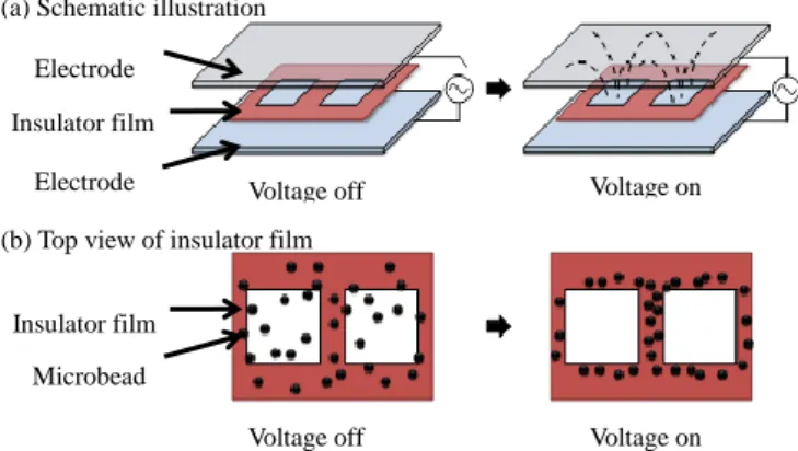
In this research, iDEP is used to collect fluorescent beads on a specific device which includes two electrodes with a patterned insulator film in between as shown in Fig. 1. When voltage is applied on the device, the charged fluorescent beads are gathered at the region of weaker electric field on the insulator film, so that the beads collection can be completed by the n-DEP force. The fluorescence signal will be enhanced by
concentrating fluorescent beads. The method can increase fluorescence intensity and sensitivity. Our device is based on the iDEP technique to detect a limited amount of streptavidin.
3. Experiment
3.1.
FabricationIndium tin oxide (ITO) is one of the most widely used transparent conducting oxides because of its electrical conductivity and optical transparency, as well as the ease of depositing and pattering. The device was fabricated on glass substrate with deposited ITO thin film. The dielectric layer of 2 μm Parylene C was deposited on ITO thin film by chmical vaporization deposition (CVD). The hydrophobic layer of Teflon is spin-coated onto the dielectric layer for increasing the contact angle of droplets.
The insulator film was fabricated by dry film photoresist (PerMX3020, DuPont). The pattern on the PerMX dry film is shown in Fig. 2. The pattern consists 25 squares arranged in a 5 ×5 array. The length of the squares is 35 μm and the interval between the squares is 60 μm. To fabricate it, a PerMX dry film was baked and is exposed by UV light (350-400 nm). Afterward, the PerMX dry film was developed by PerMX developer and rinsed by IPA.
Fig. 1. Principle behind the assay methodology, combining the insulator film and the n-DEP-based manipulation techniques. (a) Using insulator film to form nonuniform electric field. (b) Beads concentrated on the gap of a weaker electric field. Electrode Electrode Voltage on Insulator film Voltage on Voltage off Microbead Voltage off Insulator film (a) Schematic illustration
3.2.
Reagents and MaterialsBiotin covalently coupled to Fluoresbrite® YG fluorescent microbeads (2μm diameter)was purchased from Polysciences, Inc. (U.S.A.). The biotin-labeled polystyrene beads were dispensed into a microcentrifuge tube and centrifuged at 10000 ×G for 5 minutes. The supernatant in the tube was then rded. The beads are resuspended in PBS/BSA binding buffer. These steps will be repeated three times to wash the microsbeads. After the last washing, the beads can be resuspended to any volume, however higher concentrations usually work better (at least 5×10⁸ particles/ml).
Rhodamine B labeled streptavidin purchased from Invitrogen (U.S.A.) was incubated with the processed beads for 30 minutes at 4˚C to ensure that the reaction between two species was sufficient. The tube was centrifuged for 5 minutes and the supernatant in the tube was discarded. The beads are resuspended in PBS/BSA binding buffer. After repeating three times, the beads were ready for use in the following experiment.
3.3.
Experiment SettingDouble side tapes were pasted between the ITO glass plate and the insulator film as spacers. A 0.5 μl droplet was created by a pipette. Cross section of the experiment setting is shown in Fig. 3. AC voltage was applied to the sandwich constructer from a function generator. Finally, wires are connected between the chip and the control circuits. The condition of concentrated beads can be observed under a fluorescence microscope.
AC signal is produced by a function generator and passed through an amplifier to the electrodes. The electrodes were connected to a PC via an I/O card (DAQCard-USB6251). The signal is controlled with LabVIEW software (National Instruments). Detection processes was visualized by a fluorescence microscopy (IX71, Olympus) equipped with a CCD camera. The fluorescence images were analyzed by image analysis software (Image Pro Plus).
4. Results and Discussion
4.1.
Concentrate BeadsBy applying voltage, the beads would be concentrated of the gap between two square holes of the insulator film by the n-DEP force. In this experiment, two different fluorescence
streptavidin separately. Therefore, we would observe the condition of biotin-labeled polystyrene beads and streptavidin simultaneous by using different optical filter, respectively. The results are shown in Fig. 4 and the operation time was 15 minutes.
4.2.
Operation TimeThe fluorescence intensity of concentrated beads approaches to a limit after a long time. It is important to determine how
long we need to concentrate beads. For quantitative evaluation of concentrated beads, the value of fluorescence intensity was calibrated to be 0 for the initial state and 1 for the final state. We applied a 140 V voltage at 100 kHz and analyzed the
Time (min) N o rmal iz ed f lu o re sc en ce i n te n si ty
Fig. 5. The measured intensity of concentrated fluorescent beads plotted along with time. (b) (a) (d) (c) 100 μm 100 μm 100 μm
Fig. 4. The photos of concentrated beads on insulator film. (a) Before apply voltage (bright field). (b) Apply voltage to concentrate beads after 15 minutes (bright field). (c) Before apply voltage (fluorescence field). (d) Apply voltage to concentrate beads and observe Rhodamine B labeled streptavidin after 15 minutes (fluorescence field).
100 μm
Fig. 2. SEM photo of the patterned PerMX dry film.
Fig. 3. The cross section of experiment construction. Substrate Dielectric layer Electrode Hydrophobic layer Spacer Insulator film
Biotin conjugated microbead Streptavidin