Structural and electrical characteristics of atomic layer deposited high HfO
2on GaN
Y. C. Chang, H. C. Chiu, Y. J. Lee, M. L. Huang,a兲K. Y. Lee, and M. Hongb兲,c兲
Department of Materials Science and Engineering, National Tsing Hua University, Hsinchu 30012, Taiwan Y. N. Chiu and J. Kwob兲,d兲
Department of Physics, National Tsing Hua University, Hsinchu 30012, Taiwan Y. H. Wang
Department of Electrical Engineering, National Cheng Kung University, Tainan 74145, Taiwan 共Received 8 April 2007; accepted 9 May 2007; published online 4 June 2007兲
High HfO2 was deposited on n-type GaN 共0001兲 using atomic layer deposition with Hf共NCH3C2H5兲4 and H2O as the precursors. Excellent electrical properties of TiN / HfO2/ GaN metal-oxide-semiconductor diode with the oxide thickness of 8.8 nm were obtained, in terms of low electrical leakage current density 共⬃10−6A / cm2 at VFB+ 1 V兲, well behaved capacitance-voltage 共C-V兲 curves having a low interfacial density of states of 2⫻1011cm−2eV−1at the midgap, and a high dielectric constant of 16.5. C-V curves with clear accumulation and depletion behaviors were shown, along with negligible frequency dispersion and hysteresis with sweeping biasing voltages.
The structural properties studied by high-resolution transmission electron microscopy and x-ray reflectivity show an atomically smooth oxide/GaN interface, with an interfacial layer of GaON
⬃1.8 nm thick, as probed using x-ray photoelectron spectroscopy. © 2007 American Institute of Physics. 关DOI:10.1063/1.2746057兴
GaN and its related compound semiconductors, besides being used in blue light emitting diodes and lasers, have been studied for applications in high-temperature and high-power electronics because of their wide energy band gaps, high breakdown fields, and high saturation velocities in high fields. Excellent device performances have been demon- strated in the GaN-based high electron mobility transistors 共HEMTs兲, in which the Schottky-barrier gates, however, have caused a large gate leakage. There has been a great interest in the development of GaN-based metal-oxide- semiconductor field-effect-transistors 共MOSFETs兲 due to their relatively low leakage currents and capability of greater voltage swings, compared with HEMTs. In addition, the gate oxide used in surface passivation may minimize or eliminate the current collapse that occurs in unpassivated devices due to the traps existed in the regions between gate and drain.
The research on highgate dielectrics on Si as well as GaAs during the past few years has shown remarkable re- sults in achieving atomically smooth oxide/semiconductor interfaces, dielectric thickness in a nanometer range, low gate leakages, and low interfacial density of states 共Dit兲.
However, efforts of high oxides on GaN, in general, have not reached the level of material and electrical quality men- tioned above. Several high gate oxides have been studied for GaN-based MOS diodes and MOSFETs, such as Ga2O3共Gd2O3兲,1–3MgO,4Sc2O3,5,6 and Gd2O3.3,7,8
HfO2and its alloys are now the backbone for the high and metal gate technology in the recent Intel’s announcement of the 45 nm node microprocessor.9Atomic layer deposition 共ALD兲 is a chemical vapor deposition technique based on
alternative surface reactions that saturate the surface in each reaction cycle, and is now being widely used in high di- electrics deposition.
In this work, effective surface passivation of GaN has been demonstrated using ALD-HfO2. An ALD-HfO2/ GaN heterostructure, with oxide thickness of 8.8 nm共including an interfacial layer of ⬃1.8 nm兲, has shown an atomically smooth oxide/GaN interface, as demonstrated using high- resolution transmission electron microscopy 共HRTEM兲 and x-ray reflectivity共XRR兲. The interfacial layer has a compo- sition of GaON, as probed using an x-ray photoelectron spectroscopy 共XPS兲. Roughness of the oxide surface, the oxide/interfacial layer interface, and the oxide/GaN interface has been studied using XRR and determined to be 0.29, 0.5, and 0.3 nm, respectively. A low electrical leakage current density of ⬍10−8A / cm2 at 1 MV/ cm 共10−6A / cm2 at VFB+ 1 V, where VFB is the flatband voltage兲, capacitance- voltage curves with very small frequency dispersion and hys- teresis in biasing voltage sweeping, and a small interfacial density of states共Dit兲 of ⬃1011 cm−2eV−1共determined using the Terman Method兲 have also been achieved. The small Dit
demonstrated here is perhaps one of the lowest ever mea- sured in high dielectrics on GaN.
GaN 共0001兲 samples 共with an n-type doping of 5⫻1017cm−3兲 were metal organic chemical vapor deposition grown on c-plane sapphire substrates. No surface cleaning of GaN was performed prior to the ALD deposition. It is inevi- table that some contaminants will reside on top of the GaN due to air exposure. HfO2films were grown on the GaN with a wafer temperature of 200 ° C and a chamber pressure of 1 Torr using alternating pulses of tetrakis共ethylmethylamino- 兲hafnium 共TEMAH兲 and H2O as the precursors. High-purity Ar共99.999%兲 was used as diluted and purged gas. To take the process within a self-limited region, the pulse period was maintained at 2 – 3 – 2 – 3 s / cycle共i.e., 2 s each for TEMAH
a兲Also at: Research Division, National Synchrotron Radiation Research Cen- ter, Hsinchu, Taiwan.
b兲Authors to whom correspondence should be addressed.
c兲Electronic mail: [email protected]
d兲Electronic mail: [email protected]
APPLIED PHYSICS LETTERS 90, 232904共2007兲
0003-6951/2007/90共23兲/232904/3/$23.00 90, 232904-1 © 2007 American Institute of Physics
Downloaded 26 Nov 2008 to 140.116.208.52. Redistribution subject to AIP license or copyright; see http://apl.aip.org/apl/copyright.jsp
and H2O and 3 s for Ar兲 with 0.1 Torr for a partial pressure of the precursors.
Studies of electrical leakage currents and Dit’s were per- formed on TiN / HfO2/ GaN MOS diodes. Current density versus biasing field 共J-E兲 and capacitance versus voltage 共C-V兲 were measured using Agilent 4156C and 4284, respec- tively, where J is the leakage current divided by the mea- sured area and E is the biasing voltage divided by the film thickness. HRTEM specimens were prepared with mechani- cal polishing, dimpling, and ion milling using a Gatan PIPS system operated at 4 keV. The analytical work of TEM sample was performed using a Philips JEOL 2100F type TEM. XRR measurements were performed using Cu K␣ ra- diation in a standard Huber four-circle x-ray diffractometer operated at 50 kV and 200 mA. The incident light was monochromatized by a flat Ge共111兲 crystal. Two sets of slits were used to eliminate Cu K␣
2contamination and to obtain a wave-vector resolution in the scattering plane of the order 0.015 nm−1. The specular reflectivity was measured with a series of– 2scans. XRR technique serves to characterize the film thickness, the interfacial roughness, and the electron density.10,11
Fabrication of the MOS diodes is discussed in the fol- lowing. TiN 150 nm thick was deposited on the ALD-HfO2 using rf sputtering, with the pattern of the metal gate defined by photolithography. The Ohmic contact with the doped GaN layer was achieved by etching HfO2using dilute hydrofluoric acid共HF:H2O = 1 : 100兲. Subsequently, the exposed GaN sur- face contaminants were removed using dilute hydrochloric acid, followed by an e-beam evaporated metal Ti/ Al 共30/60 nm兲 on GaN. The schematic cross-sectional view of the fabricated TiN / HfO2/ GaN MOS diode is shown in Fig.
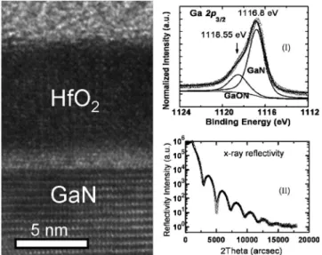
1共a兲, with the top view of the diode shown in Fig.1共b兲. Figure 2 shows a cross-sectional HRTEM image of an amorphous ALD-HfO2 film on GaN. The oxide consists of two layers with an overall thickness measured by TEM to be 8.8 nm. The top layer is HfO2⬃7.0 nm thick, and the bot- tom interfacial layer is⬃1.8 nm thick, with a composition of GaON. The different contrasts are due to a heavier mass of Hf in comparing with that of Ga. The composition of the interfacial layer between HfO2and GaN was analyzed using XPS with an Al K␣ source 共photon energy 1486.6 eV兲, as shown in the inset共I兲 of Fig.2. The broad Ga 2p peak could be deconvoluted to the peak共1116.8 eV兲 of bulk GaN sub- strate and the Ga oxynitride peak共1118.55 eV兲. There is a chemical shift of 1.75 eV between the two peaks.
An XRR fringe pattern is shown in the inset共II兲. From the period of oscillations, the oxide film thickness, and the values of the roughness of the oxide surface and the interface between the oxide and GaN have been calculated using the
theoretical fitting model. An interfacial roughness of a range of 0.3 nm has been obtained in the HfO2/ GaN interface. It is interesting to observe that the roughness on top of HfO2and the oxide/GaN interface is similar of⬃0.3 nm, indicating the existence of a correlation between the oxide surface and the interface. The atomic-scale correlation was also observed earlier in Au/ GaAs, a metal/semiconductor heterostructure.10 A rougher interface共⬃0.5 nm兲 between HfO2and the inter- facial layer may indicate chemical reactions among TEMAH, H2O, and GaN native oxides during the ALD process.
In a separate experiment, nanometer thick HfO2 films were deposited on GaN with electron beam evaporation un- derultra high vacuum共UHV兲.12 The interface is atomically sharp, without any interfacial layer between GaN and the UHV-deposited HfO2, as studied using HRTEM, and the XRR measurements whose fitting involves no interfacial layer. The XPS investigation also confirms this. Comparing the results of ALD- and UHV-deposited HfO2 on GaN, the interfacial layer of GaON occurring in the former case has been formed during the initial stage of the ALD process, similar to the formation of silicate in ALD-HfO2on Si.
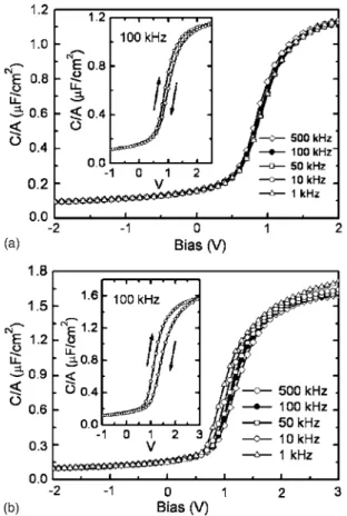
The TiN / HfO2/ GaN MOS diode after 375 C annealing in forming gas for 20 min shows well behaved C-V charac- teristics of varying frequency from 1 to 500 kHz with accu- mulation, depletion, and a dielectric constant of 11.6, as ex- hibited in Fig. 3共a兲. Note that very little dispersion in the accumulation regime was observed along with the very small hysteresis with sweeping biasing voltages, as shown in the inset of Fig.3共a兲. Annealing at 600 ° C for 10 min in a pure argon gas flow did increase the dielectric constant from 11.6 to 16.5, and the EOT is correspondingly decreased from 2.96 to 2.08 nm, where EOT is the equivalent oxide thick- ness, defined as SiO2 共thickness of high dielectrics兲/
共high兲. A slight increase in dispersion and hysteresis was observed, as shown in Fig. 3共b兲 and its inset. Further- more, from the C-V curves a very low Dit, roughly 2⫻1011cm−2eV−1 at midgap was obtained using the Ter- man method, with a detailed calculation discussed in Ref.13.
The low Dit value is similar to what was obtained in the UHV-Ga2O3共Gd2O3兲/GaN.14,15
FIG. 1. 共a兲 Schematic cross-sectional view of the fabricated TiN / HfO2/ GaN MOS diode, with the top view shown in共b兲.
FIG. 2. Cross-sectional high-resolution TEM image of HfO28.8 nm thick on GaN. Inset 共I兲: the XPS spectrum of Ga 2p3/2 core level shows the existence of an interfacial layer of GaON.共II兲: low angle x-ray reflectivity of HfO2on GaN, with experimental data共dots兲 and a theoretical fit 共line兲.
232904-2 Chang et al. Appl. Phys. Lett. 90, 232904共2007兲
Downloaded 26 Nov 2008 to 140.116.208.52. Redistribution subject to AIP license or copyright; see http://apl.aip.org/apl/copyright.jsp
Figure4shows the J-E curves of MOS diodes after an- nealing at 375 ° C in forming gas and at 600 ° C in pure argon. The leakage current density at VFB+ 1 V is 1.4
⫻10−6 and 2⫻10−6A / cm2 for sample annealed at 375 and 600 ° C, respectively. The corresponding electrical fields for VFB+ 1 V are 2.22 and 2.45 MV/ cm for sample annealed at 375 and 600 ° C, respectively, as labeled in Fig.4. The leak- age current density increased after 600 ° C annealing may have been caused by the formation of polycrystalline HfO2 from amorphous films.
Asymmetrical characteristics of J-E curves under the forward and reverse biases were obtained, which were also observed previously in thicker dielectric films.6,15,16 The leakage current densities in the reverse bias remain very low even at high electrical fields, most likely due to extremely low minority carriers available, as explained with the very low intrinsic carrier concentration 共⬃10−10cm−3兲 in GaN.
However, the higher leakage current densities at the forward bias are resulted from the transport of the majority carriers.
In conclusion, the electrical and structural properties achieved in this work in employing ALD-HfO2on GaN have approached the level of high dielectrics on Si and GaAs, namely, a low Dit of ⬃2⫻1011cm−2eV−1, a low leakage current density of 10−7– 10−8 A / cm2 at 1 MV/ cm for an
8.8 nm thick oxide共an EOT of 2.08 nm兲, the thermodynamic stability of the heterostructure共with 600C annealing兲, high
value, and negligible frequency dispersion in the C-V mea- surements.
The work was supported by the National Nano projects 共NSC 95-2120-M-007-006 and NSC 95-2120-M-007-005兲 of National Science Council in Taiwan.
1M. Hong, K. A. Anselm, J. Kwo, H. M. Ng, J. N. Baillargeon, A. R.
Kortan, J. P. Mannaerts, A. Y. Cho, C. M. Lee, J. I. Chyi, and T. S. Lay, J.
Vac. Sci. Technol. B 18, 1453共2000兲.
2F. Ren, M. Hong, S. N. G. Chu, M. A. Marcus, M. J. Schurman, A. Baca, S. J. Pearton, and C. R. Abernathy, Appl. Phys. Lett. 73, 3893共1998兲.
3T. S. Lay, Y. Y. Liao, W. H. Hung, M. Hong, J. Kwo, and J. P. Mannaerts, J. Cryst. Growth 278, 624共2005兲.
4Y. Irokawa, Y. Nakano, M. Ishiko, T. Kachi, J. Kim, F. Ren, B. P. Gila, A.
H. Onstine, C. R. Abernathy, S. J. Pearton, C.-C. Pan, G.-T. Chen, and J.-I.
Chyi, Appl. Phys. Lett. 84, 2919共2004兲.
5J. Kim, R. Mehandru, B. Luo, F. Ren, B. P. Gila, A. H. Onstine, C. R.
Abernathy, S. J. Pearton, and Y. Irokawa, Appl. Phys. Lett. 81, 373 共2002兲.
6C. Liu, E. F. Chor, L. S. Tan, and Y. Dong, Appl. Phys. Lett. 88, 222113 共2006兲.
7M. Hong, A. R. Kortan, H. M. Ng, J. Kwo, S. N. G. Chu, J. P. Mannaerts, A. Y. Cho, C. M. Lee, J. I. Chyi, and K. A. Anselm, J. Vac. Sci. Technol.
B 20, 1274共2002兲.
8T. Fluckiger, M. Erbudak, A. Hensch, Y. Weisskopf, M. Hong, and A. R.
Kortan, Surf. Interface Anal. 34, 441共2002兲.
9http://www.intel. com/pressroom/archive/releases/20060125comp.htm.
10D. Y. Noh, Y. Hwu, H. K. Kim, and M. Hong, Phys. Rev. B 51, 4441 共1995兲.
11Y. L. Huang, P. Chang, Z. K. Yang, Y. J. Lee, H. Y. Lee, H. J. Liu, J. Kwo, J. P. Mannaerts, and M. Hong, Appl. Phys. Lett. 86, 191905共2005兲.
12W. C. Lee, Y. C. Chang, Y. J. Lee, T. D. Lin, H. C. Chiu, J. Kwo, Y. H.
Wang, and M. Hong共unpublished兲.
13C. P. Chen, Y. J. Lee, Y. C. Chang, Z. K. Yang, M. Hong, J. Kwo, H. Y.
Lee, and T. S. Lay, J. Appl. Phys. 100, 103508共2006兲.
14T. S. Lay, W. D. Liu, M. Hong, J. Kwo, and J. P. Mannaerts, Electron.
Lett. 37, 595共2001兲.
15Y. C. Chang, Y. J. Lee, Y. N. Chiu, T. D. Lin, S. Y. Wu, H. C. Chiu, J.
Kwo, Y. H. Wang, and M. Hong, J. Cryst. Growth 301/302, 390共2007兲.
16C. T. Lee, H. Y. Lee, and H. W. Chen, IEEE Electron Device Lett. 24, 54 共2003兲.
FIG. 4. Leakage current density J 共A/cm2兲 vs E 共MV共cm兲 for TiN / HfO2/ GaN MOS diode in different thermal processes.
FIG. 3. C-V curves of TiN / HfO2/ GaN MOS diode under various frequen- cies from 1 to 500 kHz, with共a兲 annealing at 375 and 共b兲 600 °C.
232904-3 Chang et al. Appl. Phys. Lett. 90, 232904共2007兲
Downloaded 26 Nov 2008 to 140.116.208.52. Redistribution subject to AIP license or copyright; see http://apl.aip.org/apl/copyright.jsp