Influence of Process Flow on the Characteristics of Strained-Si
nMOSFETs
K. T. Lam,aS. L. Wu,bS. J. Chang,c,zY. P. Wang,cand U. H. Liawd a
Department of Information Communication, Leader University, Tainan 70970, Taiwan b
Department of Electronic Engineering, Cheng Shiu University, Niaosong, Kaohsiung 833, Taiwan c
Institute of Microelectronics and Department of Electrical Engineering, Center for Advanced Optoelectronic Technology, National Cheng Kung University, Tainan 701, Taiwan
d
Department of Avionics, China Institute of Technology, Hsinchu 312, Taiwan
We developed a process design that uses epitaxial growth of strained-Si layers after shallow trench isolation 共STI兲 and well implantation to improve the drive current of n-type metal-oxide-semiconductor field effect transistors共nMOSFETs兲. Due to the significantly reduced thermal budget, we can minimize the degree of partial relaxation in strained-Si layers based on state-of-the-art MOSFET integration technique. Experimental results show that strained-Si devices fabricated by this flow exhibit enhanced saturated drive currents, up to 12% higher than that of strained-Si device with epitaxial growth of strained-Si layers before STI and well implantation.
© 2007 The Electrochemical Society. 关DOI: 10.1149/1.2775427兴 All rights reserved.
Manuscript submitted May 11, 2007; revised manuscript received June 26, 2007. Available electronically August 23, 2007.
Methods of optimizing channel mobility need to be explored in order to overcome the limitations on the scaling down of devices and further improve the speed of complementary metal-oxide-semiconductor共CMOS兲 circuits. A promising candidate to reach this demand is to exploit the strain-induced band-structure modification. The use of a strained-Si channel for n-type metal-oxide-semiconductor field effect transistors 共nMOSFETs兲1-3 has made great improvements on dc characteristics due to its potentially higher electron mobility. Enhanced carrier mobility using a tensile strained Si results principally from a reduction of the in-plane carrier effective mass and a reduction of intervalley scattering. Therefore, by fabricating MOSFET devices on the strained-Si layer, faster CMOS devices and performance enhancements are predicted with-out the high costs associated with aggressive geometric scaling. However, currently most studies4-6 use a simplified standard MOS fabrication process based on reduced thermal budgets during the various processing steps to implement strained-Si nMOSFETs, par-ticularly to avoid high-temperature shallow trench isolation 共STI兲 commonly used in advanced integration processes, which leads to restriction in device implementation. Therefore, how to introduce the STI technology into strained-Si nMOSFET and make this flow useful for nanoscale transistors in advanced logic technologies are currently important issues. In this paper, strained-Si nMOSFETs pre-pared by process integration flows共selective growth of Si layer on SiGe virtual substrate post-STI and well implantation兲 has been fab-ricated. Compared to devices with epitaxial strained-Si layer before STI and well implantation, this process technology seems to effi-ciently reduce thermal budgets and provide an additional enhance-ment 共up to 15%兲 in long-channel mobility. This additional in-creased mobility behavior is translated into a 12% higher on-state current for the long-channel devices and a 6% higher on-state cur-rent 共VGS− VTH= 1 V and VDS= 1 V兲 for devices down to 0.24m. Obviously, applying the modified STI technology flow to strained-Si nMOSFET fabricated is very suitable for state-of-the-art CMOS process.
Experimental
The epitaxy structures investigated in this work were fabricated by a commercially available multi-wafer ultrahigh vacuum chemical vapor deposition共CVD兲 system on Si共100兲 10–15 ⍀ cm substrate. Silane and germane were used as the Si and Ge precurors, respec-tively. The Si substrates were subjected to a precleaned process with HF-dip solution to reduce the accumulation of contamination by removing the surface native oxide and forming hydrogen passivated
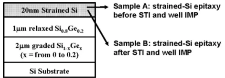
surface. After the precleaning step, the wafers were loaded into the loading chamber and then transferred to the reaction chamber for epitaxial growth. Structures first consist of a linearly graded Si1−xGexbuffers layers with the x content increased from 0 to 20% over the thickness of 2m, followed by an undoped 1-m-thick relaxed Si0.8Ge0.2virtual substrate. The SiGe epitaxial layers were
grown at 675°C. After that, same structure parameters with different process flows are adopted to identify the impact of high-temperature STI technology on the device characteristics. Herein, a 20 nm thick strained-Si layer was grown on relaxed Si0.8Ge0.2 virtual substrate. Then, the active areas were sequentially defined by the shallow trench isolation共STI兲, well implantation for the A sample. For the sample B, after STI and well implantation, selective epitaxy of strained-Si layer was then grown on the virtual substrate. The STI process included linear oxide deposition共920°C, 20 s兲, linear oxide postannealing 共990°C, 30 min兲 and high density plasma 共HDP兲-CVD oxide rapid thermal annealing 共RTA兲 共1000°C, 20 s兲. The p-well formation was implanted with 5⫻ 1013atoms/cm2 boron
and well-implant annealing was done at 1000°C for 12 s. Figure 1 shows the schematic diagram of different process flow sequences.
After that, all samples, including a Si control, were processed to produce nMOSFETs using the same Si CMOS process flow for comparison. Gate oxide of 2.2 nm was formed by wet, atmospheric pressure oxidation at 800°C for 30 min to minimize interdiffusion of the as-grown layer structure. Afterward, poly-Si gate was depos-ited and etched. This was followed by source/drain extensions and halos implants, spacer formation. After the gate spacer etching, a thin Si layer was grown in the source/drain region by a selective epitaxy growth process to reduce the contact resistance. After source/drain rapid thermal annealing共RTA兲 at 1050°C for 6 s was used to activate the implantations. Co silicides were formed in suc-cessive rapid thermal anneals at 480°C for 35 s and 830°C for 25 s. The other procedures were based on standard backend process.
z
E-mail: changsj@mail.ncku.edu.tw
Figure 1. The schematic diagram of the strained-Si transistors process
se-quences.
Electrochemical and Solid-State Letters, 10共11兲 H331-H333 共2007兲
1099-0062/2007/10共11兲/H331/3/$20.00 © The Electrochemical Society H331
Results and Discussion
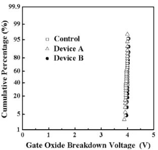
It is noted that the high-temperature thermal processing not only enhanced Ge up-diffusion into the Si6 but also induced partially strained-Si relaxation,7which are responsible for the mobility deg-radation. Ge up-diffusion becomes severe when strained-Si layer is less than 10 nm.8This is attributed to that at high-temperature pro-cess Ge from the underlying SiGe diffuse up into the strained-Si channel and segregated at the strained-Si/oxide interface. Conse-quently, it will lead to an increased fixed oxide charge and high trap density at SiO2/Si interface, which result in a reduced gate-oxide breakdown voltage. However, strained-Si layer chosen at 20 nm thickness in our devices is enough immunity against Ge out-diffusion to gate oxide and is confirmed by comparable oxide break-down voltage distribution共Fig. 2兲. Therefore, the effect of the Ge up-diffusion can be neglected in these devices.
The output current-voltage characteristics of strained-Si nMOSFET with the STI process are shown in Fig. 3. Evidently, both strained-Si nMOSFETs exhibit larger enhancement in driving cur-rent at a given degree of gate overdrive, which are responsible for the “high mobility” of the stained-Si channel共Fig. 4兲. Moreover, as compared to device A with pre-STI and well implantation, device B provides an effective enhancement in driving current of 12% for the long-channel length共L = 10 m兲 and of 6 % for the channel length down to 0.24m, at the same gate overdrive 共Vgs− Vth= 1 V兲. We believe that such an improvement in device performance is attrib-uted to the elimination of the effects of high-temperature STI pro-cess and well implantation on sample B. On the other hand, 15% degradation of channel mobility in sample A, as experimentally ob-served in Fig. 4, revealed that the strained-Si layer undergoes the additional high-temperature STI and well implantation process which leads to a decreased stress level in the Si cap layer. Conse-quently, an increase in the degree of strained-Si relaxation is accom-panied by more misfit and threading dislocations formation which not only reduced the carrier mobility by scattering but also caused an increase in the leakage currents, as mentioned by the previous report.7 Moreover, inefficient strain-induced energy band splitting also degrades mobility enhancement.
To further investigate the influence of different STI process se-quences in this paper on the electrical characteristics of the strained-Si device, the threshold voltage共VTH兲 roll-off as a function
of gate length for the strained-Si with gate width of 10m is shown in Fig. 5. Noted that the VTHroll-off characteristics for sample B is
compared to Si control. However, observed a lower VTHand sharper roll-off curve in sample A, especially at such wider gate width,
indicates that the post-STI induces partial relaxation of strained-Si layers, resulting in more misfit dislocations between source and drain, which serve as a rapid diffusion path. Therefore, the more localized diffusion along these misfit dislocations cores is respon-sible for the larger leakage current mechanism for sample A.
Conclusion
Strained-Si nMOSFET structures prepared by different STI pro-cess were fabricated. By appropriately modifying the STI propro-cess
Figure 2. Comparison of the nMOSFETs gate oxide breakdown voltage
distribution in strained-Si and Si control.
Figure 3. IDS-VDScharacteristics of the fabricated strained-Si and Si control devices with channel lengths of共a兲 10 m and 共b兲 0.24 m, respectively.
Figure 4. Effective mobility for strained-Si nMOSFETs as a function of
effective field.
H332 Electrochemical and Solid-State Letters, 10共11兲 H331-H333 共2007兲
H332
sequences, the significant drive current and mobility enhancement has been obtained. Improved characteristics in sample B indicate
that devices with new process sequences exhibit the controlled mis-fit dislocations in strained-Si layers and show a great flexibility for developing high-performance strained-Si CMOS.
Acknowledgments
This work was supported by the National Science Council 共NSC兲, Taiwan, under contract no. NSC 95-2221-E-230-031.
National Cheng Kung University assisted in meeting the publication costs of this article.
References
1. W. C. Hua, M. H. Lee, P. S. Chen, M. J. Tsai, and C. W. Liu, IEEE Electron Device
Lett., 26, 667共2005兲.
2. S. H. Olsen, A. G. O’Neill, L. S. Driscoll, K. S. K. Kwa, S. Chattopadhyay, A. M. Waite, Y. T. Tang, A. G. R. Evans, D. J. Norris, A. G. Cullis, D. J. Paul, and D. J. Robbins, IEEE Trans. Electron Devices, 50, 1961共2003兲.
3. T. Irisawa, T. Numata, N. Sugiyama, and S. Takagi, IEEE Trans. Electron Devices, 52, 993共2005兲.
4. K. Rim, J. L. Hoyt, and J. F. Gibbons, IEEE Trans. Electron Devices, 47, 1406 共2000兲.
5. N. Sugii, D. Hisamoto, K. Washio, N. Yokoyama, and S. Kimura, IEEE Trans.
Electron Devices, 49, 2237共2002兲.
6. W. C. Hua, M. H. Lee, P. S. Chen, S. Maikap, C. W. Liu, and K. M. Chen, IEEE
Electron Device Lett., 25, 693共2004兲.
7. S. B. Samavedam, W. J. Taylor, J. M. Grant, J. A. Smith, P. J. Tobin, A. Dip, A. M. Phillips, and R. Liu, J. Vac. Sci. Technol. B, 17, 1424共1999兲.
8. Y. P. Wang, S. L. Wu, and S. J. Chang, Jpn. J. Appl. Phys., Part 2, 44, L1248 共2005兲.
Figure 5. Threshold voltage as a function of gate length for the strained-Si
with gate width of 10m.
H333
Electrochemical and Solid-State Letters, 10共11兲 H331-H333 共2007兲 H333