Enhancement of the light output performance for GaN-based light-emitting diodes by bottom pillar structure
Chien-Chun Wang
Institute of Electro-Optical Science and Engineering, National Cheng-Kung University, Tainan City, Taiwan 701, Republic of China
Han Ku
Institute of Microelectronics, Department of Electrical Engineering, National Cheng-Kung University, Tainan City, Taiwan 701, Republic of China
Chien-Chih Liu
Department of Electrical Engineering, Nan Jeon Institute of Technology, Tainan County, 737 Taiwan, Republic of China
Kwok-Keung Chong
Department of Microelectronics Engineering, National Kaohsiung Marine University, Kaohsiung City, 811 Taiwan, Republic of China
Chen-I Hung
Department of Mechanical Engineering, National Cheng-Kung University, Tainan City, Taiwan 701, Republic of China
Yeong-Her Wang
Institute of Electro-Optical Science and Engineering, National Cheng-Kung University, Tainan City, Taiwan 701, Republic of China
Mau-Phon Hounga兲
Institute of Microelectronics, Department of Electrical Engineering, National Cheng-Kung University, Tainan City, Taiwan 701, Republic of China
共Received 22 June 2007; accepted 28 August 2007; published online 18 September 2007兲 A three-dimensional model with finite difference and time domain was established to investigate the enhancement of the light output intensity of GaN light-emitting diodes共LEDs兲 with bottom pillar 共BP兲 structure. Through comparing the normalized light extraction intensity of GaN LEDs with or without BP in different dimensions, the theoretical results show that the light output intensity in the LED with BP structure involved could be enhanced by about 30%. The influence of BP structure on the light output intensity of a LED could be explained by the physical model of light interaction. In addition, the experimental results also show the same trend to the theoretical calculations. © 2007 American Institute of Physics. 关DOI:10.1063/1.2786015兴
Applications of GaN-based light emitting diodes共LEDs兲 are commonly applied in traffic signals, outdoor full-color displays, backlight units in liquid crystal displays, general illumination, etc. For the demand of having higher light out- put power at a lower power consumption, the conventional GaN-based LED chips fabricated on the sapphire substrate could still not achieve such a requirement because of having a relatively low value of the external quantum efficiency 共ext兲. The main reason for such a low efficiency value is the great extent of the total internal reflection the interface of GaN/air. It thus limits the extraction efficiency to about 1 / 4n2 共about 4%兲 in the GaN semiconductor slab. Conse- quently, structural design and fabrication technology of LEDs for higher light extraction are emerged as great interests.1–3
Several approaches have been reported to improve the above mentioned situation. By using truncated inverted pyra- mid geometry, the mean photon path length within the crystal is decreased to reduce the effects of internal loss mechanisms.4 Through photonic crystals5 and random sur- face texturing,6,7 designs could allow light to escape more
easily. However, these structural modifications for the light extraction improvements are mainly focused on the top of LED chips, whereas by reducing the light escape from the substrate could also help a LED to improve its light output power to a certain extent. For example, patterned sapphire substrate 共PSS兲 has been proposed for this purpose.3,8 The original aim of PSS is to reduce the threading dislocation 共TD兲 densities during the growth of GaN epilayer. Because of reducing the TDs in the GaN microstructure, PSS could result in improving the internal quantum efficiency. In addi- tion, it has been proven that a PSS could cause the scattering light intensity associated with its surface roughness which directly improves the light output power of the LED in a certain extent.9,10 In this work, a theoretical model to study the influence of light output intensity by the substrate with geometric pattern design关bottom pillar 共BP兲 substrate兴 was proposed to achieve an optimal design for light extraction of a GaN LED. In combination with the ray-tracing method based on Snell’s law and the finite difference and time domain11 共FDTD兲 mathematical technique, a three- dimensional theoretical model is established to investigate the influences of the structural parameters, such as diameter and spacing of the bottom pillars on the light output inten-
a兲FAX: 866-6-2080598. Electronic mail: [email protected].
APPLIED PHYSICS LETTERS 91, 121109共2007兲
0003-6951/2007/91共12兲/121109/3/$23.00 91, 121109-1 © 2007 American Institute of Physics
Downloaded 05 Aug 2009 to 140.116.208.35. Redistribution subject to AIP license or copyright; see http://apl.aip.org/apl/copyright.jsp
sity. Furthermore, the experimental works were also con- ducted as for comparing the theoretical results.
In the following theoretical calculations, a three- dimensional model based on the FDTD on solving Max- well’s equations with periodic boundary condition intro- duced by the two-dimensional hexagonal array of the bottom pillar structure was employed to calculate the light field in- tensity distributed inside the LED. Such a device structure is simply shown in Fig. 1. The sapphire substrate has a two- dimensional hexagonal pillar structure. The average distance between neighboring hexagonal pillars is 1.75– 2.75m.
The stimulations are done using a commercial software package.12 By the FDTD technique, it effectively provides for studying the propagation of light in a wide variety of photonic structures. In simulating the light source of the ac- tive region, the point dipole oscillator is used as a radiating source and is continuously excited so that the total power emitted from the active region is assumed constant in all directions.13 Moreover, the thickness of this active region is relatively small as compared with the device thickness. The multiple quantum well can be treated as a single epitaxial layer with a collection of point dipoles.11 Over 10 000 TE- polarized point dipoles were used in the following analysis by locating them evenly on the active layer plane. The reason for analyzing the TE-polarized light here is due to the fact that light emitted from a quantum well sandwiched between two dielectric layers would have a similar polarization.14 There is also on experimental evidence that TE polarization dominates in the InGaN / GaN quantum-well blue LEDs.15To reduce the load of computation, the simulated LED with BP structure is subjected to a periodic boundary condition which neglects the limitations of finite x-y plane but preserves the periodic distribution of the BP structure on the surface of the sapphire substrate. Finally, the emitted light power was theo- retically evaluated by means of the Poynting vector.
In fabricating a LED as for easy comparing with the theoretical results, the sapphire substrate was etched by in- ductively coupled plasma dry etching to form an array of hexagonal patterns of BP structure with a standard photoli- thography process. The etching depth for bottom pillar struc- ture was controlled by about 3500– 4500 Å. After fabricating the BP structure, the GaN LED was grown on the etched sapphire by metal-organic chemical-vapor deposition. The
device consists of a 1m low-temperature-deposited GaN buffer layer, a 3.5m Si doped n-GaN layer 共3
⫻1018cm−3兲, five periods of InGaN/GaN multiple quantum well active layers, and a 0.2m Mg-doped p-GaN layer, as also shown in Fig1.
As clearly revealed in Fig.2, the sapphire etched with a pillar structure on its surface has a sidewall angle of 111.9°.
Additionally, the top side diameter and the height of the pil- lar are 1378.1 and 356.3 nm, respectively. For theoretical calculations, the average value of 0.45m obtained in the experiment as adopted for the depth of the bottom pillar structure in order to analyze the influence of bottom pillar structure on the light output intensity. The diameter of the pillar is a, the spacing of the pillar is b, and the pitch of the pillars is d with d = a + b. With a fix value of 1.5m for the diameter of the pillar, the value of spacing b is intentionally adjusted from 0.25 to 1.25m in the following calculations.
The normalized light intensity illustrated in Fig.3 is evalu- ated by comparing the light power of LED with BP structure to that of LED without BP structure. The LED has a peak value of about 30% enhancement at the d / b ratio of 3. The result is obtained at the condition of the spacing b just equal to a half of the diameter a. Obviously, the bottom pillar structure could enhance the light extraction of LEDs. The above simulation results could be qualitatively explained by means of the double-slit model. Based on this model, the light intensity is expressed as16
I = 4A02sin2
2 cos2␥, 共1兲
where
FIG. 1. 共a兲 Illustration of the vertical layer structure of LED with pillar structure fabricated on top of sapphire.共b兲 Schematics of three-dimensional view of the etched sapphire with pillar structure and top view of the hex- agonal array configuration of pillar structure. The anglecorresponds to the angle between the vertical z axis and the direction of diffracted light by bottom pillar structure; parameters b and d directly correspond to the spac- ing and the pitch of pillars.
FIG. 2. Scanning electron microscope of the side view of etched sapphire substrate having a sidewall angle of 111.9°. The top side diameter and the height of the pillar are 1378.1 and 356.3 nm, respectively. For theoretical calculations, the diameter of the pillar is a, the spacing of the pillar is b, and the pitch of the pillars is assigned as d with d = a + b.
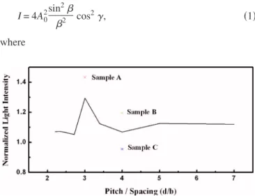
FIG. 3. Comparisons of the normalized light power extraction against pitch to spacing共d/b兲 ratio between the theoretical calculations and experimental results 共sample A: d/b=1.5/0.5, sample B: d/b=2/0.5, and sample C:
d / b = 4 / 1兲. The normalized light intensity is evaluated by the light power of LED with BP structure to that of LED without BP structure.
121109-2 Wang et al. Appl. Phys. Lett. 91, 121109共2007兲
Downloaded 05 Aug 2009 to 140.116.208.35. Redistribution subject to AIP license or copyright; see http://apl.aip.org/apl/copyright.jsp
=
b sin and
␥=
d sin.
Here I is the light field intensity, A0is the amplitude, b is the slit width, and d is the separation of the slits. For the pillar structure, parameters b and d directly correspond to the spac- ing and the pitch of pillars, as shown in Fig.2. The angle in Eq. 共1兲 corresponds to the angle between the vertical z axis and the direction of the diffracted light by bottom pillar structure, as illustrated in Fig. 1共b兲. As predicted by this equation, the factor共sin2兲/2corresponds to the width b of a slit, which is the spacing of the pillar, and the term cos2␥ is the characteristic of the interference pattern. The product result of共sin2兲/2cos2␥ is the central maximum of a slit which acts as an envelope of the interference pattern. The effect of decreasing b which causes the full width at half maximum of the envelope mainly concentrates on the loca- tion relative to the zeroth order and results in the strongest light intensity that only happened for this order. Furthermore, through the reflection induced by the scattering of the BP structure, a large amount of light power could be reflected back to the top side of a LED which could then enhance the light power output from the top side of the device.17There- fore, an initial decrease of the spacing of pillar b favors the enhancement of light power output of the LED. An optimum normalization value or a peak value of light power extraction is then obtained. After this peak value, a further decrease of b has reached to a value that it makes the term共sin2兲/2 approximately equal to 1; the light intensity is then strongly dominated by the interference term cos2␥. Under this situa- tion, the number of interference slits per unit phase angle now increases with a further decrease of b. The light inten- sity allocating to the zeroth order should be relatively dimin- ished with an increase of the d / b ratio 共because of an in- crease in the number of interference slits兲. The overall result causes the light reflection induced by the scattering of the BP structure to be reduced to a great extent. Thus, the light power vertically reflected back to the top side of a LED should be diminished with a further decrease of b.
To compare with the simulated results, three sets of samples A, B, and C were fabricated with the pitch to spac- ing ratios 共d/b, length measured in nanometers兲 of 3共d/b
= 1.5/ 0.5兲, 4共d/b=2/0.5兲, and 4共d/b=4/1兲, respectively.
The normalized light output intensity measurements of these samples are also shown in Fig.3. Since the central wave- length of the LED without BP structure is located at 450 nm, the light output intensities of the samples with BP structure are all normalized to that of the LED without BP structure at 450 nm, for comparison. Focusing on the samples A共with d / b ratio of 3兲 and B 共with d/b ratio of 4兲, sample A has a better improvement than sample B, showing the same trend to the theoretical calculations. Under the same d / b ratio of 4 for samples B and C, sample B has a higher normalization value of about 24% than sample C, which reveals the fact that sample B has better light output intensity than sample C.
It implies that the BP structure designed for sample C con- versely makes it to have lower light output intensity than the device without BP structure. Obviously, sample C is inten-
tionally fabricated with two times spacing larger than that in sample B. This result could be well explained by the periodic distribution of BP structure. Under the limit of the same size for a LED, an increase of both the diameter of the pillar and the spacing results in a decrease of the number of BP. This directly diminishes the probability of light diffraction mecha- nism caused by the BP structure. Therefore, a decrease of BP density on the sapphire substrate directly reduces the light reflection by the light scattering of the BP structure.
A three-dimensional FDTD model was implemented to investigate the enhancement of light power extraction of a GaN LEDs with bottom pillar. The relationship of the diam- eter and the spacing of bottom pillar had been discussed on the influence on the light output intensity. According to the theoretical calculations, an optimum pitch to spacing 共d/b兲 ratio of bottom pillars of 3 causes the device having the light output intensity to be enhanced by about 30%. The influence of BP structure on the light output intensity of a LED could be explained by the physical model of light interaction. In addition, the experimental results also show the same trend to the theoretical calculations.
This work was supported by the National Science Coun- cil of Taiwan under Contract Nos. NSC-95-2221-E-006- 353-, NSC-96-2221-E-006-082-MY2, and NSC-96-2221-E- 232-001-. The authors are grateful to the National Center for High-Performance Computing for computer time and facili- ties and to Shi-Qing Chen, Jan-Dar Guo, and Wei-Chih Lai, Epitech Technology Corporation workers, for experimental assistance.
1C.-C. Liu, Y.-H. Chen, M.-P. Houng, Y.-H. Wang, Y.-K. Su, W.-B. Chen, and S.-M. Chen, IEEE Photonics Technol. Lett. 16, 1444共2004兲.
2M. Yamada, T. Mitani, Y. Narukawa, S. Shioji, I. Niki, S. Sonobe, K.
Deguchi, M. Sano, and T. Mukai, Jpn. J. Appl. Phys., Part 2 41, L1431 共2002兲.
3Y. J. Lee, J. M. Hwang, T. C. Hsu, M. H. Hsieh, M. J. Jou, B. J. Lee, T. C.
Lu, H. C. Kuo, and S. C. Wang, IEEE Photonics Technol. Lett. 18, 1152 共2006兲.
4M. R. Krames, M. Ochiai-Holcomb, G. E. Höfler, C. Carter-Coman, E. I.
Chen, I.-H. Tan, P. Grillot, N. F. Gardner, H. Chui, J.-W. Huang, S. A.
Stockman, F. A. Kish, M. G. Crawford, T. S. Tan, C. P. Kocot, M. Hue- schen, J. Posselt, B. P. Loh, G. Sasser, and D. Collins, Appl. Phys. Lett.
75, 2365共1999兲.
5M. Borodilsky, T. F. Kraus, R. Coccioli, R. Vrijen, R. Bhat, and E.
Yablonovitch, Appl. Phys. Lett. 75, 1036共1999兲.
6R. Windisch, C. Rooman, S. Meinlschmidt, P. Kiesel, D. Zipperer, G. H.
Döhler, B. Dutta, M. Kuijk, G. Borghs, and P. Heremans, Appl. Phys. Lett.
79, 2315共2001兲.
7J. M. Lupton, B. J. Matterson, I. D. W. Samuel, M. J. Jory, and W. L.
Barnes, Appl. Phys. Lett. 77, 3340共2000兲.
8K. Tadatomo, H. Okagawa, Y. Ohuchi, T. Tsunekawa, Y. Imada, M. Kato, and T. Taguchi, Jpn. J. Appl. Phys., Part 2 40, L583共2001兲.
9D. S. Wuu, W. K. Wang, W. C. Shin, R. H. Horng, C. E. Lee, W. Y. Lin, and J. S. Fang, IEEE Photonics Technol. Lett. 17, 288共2005兲.
10C. C. Sun, C. Y. Lin, T. X. Lee, and T. H. Yang, Opt. Eng.共Bellingham兲 43, 1700共2004兲.
11W. J. Choi, Q.-H. Park, D. Kim, H. Jeon, C. Sone, and Y. Park, J. Korean Phys. Soc. 49, 877共2006兲.
12FULLWAVE 5.0 User’s Manual, RSoft Design Group, Inc., Ossining, NY, USA, 2006.
13L. A. Coldren and S. W. Corzine, Diode Lasers and Photonic Integrated Circuits, 2nd ed.共Wiley, New York, 1995兲, pp. 148–153 and 518–525.
14S. Fan, P. R. Villeneuve, J. D. Joannopoulos, and E. F. Schubert, Phys.
Rev. Lett. 78, 3294共1997兲.
15J. Shakya, K. Knabe, K. H. Kim, J. Li, J. Y. Lin, and H. X. Jiang, Appl.
Phys. Lett. 86, 091107共2005兲.
16F. A. Jenkins and H. E. White, Fundamentals of Optics, 4th ed.共McGraw- Hill, New York, 1976兲, p. 338.
17C.-H. Chao, S. L. Chuang, and T.-L. Wu, Appl. Phys. Lett. 89, 091116 共2006兲.
121109-3 Wang et al. Appl. Phys. Lett. 91, 121109共2007兲
Downloaded 05 Aug 2009 to 140.116.208.35. Redistribution subject to AIP license or copyright; see http://apl.aip.org/apl/copyright.jsp