IEEE Transaction on Power Electronics
Title: A Novel High Step-Up DC-DC Converter for Microgrid System Manuscript ID: TPEL-Reg-2010-06-0460
Authors: Yi-Ping Hsieh, Email: [email protected]
Jiann-Fuh Chen, Member, IEEE, Email: [email protected] Tsorng-Juu Liang, Member, IEEE, Email: [email protected] Lung-Sheng Yang, Email: [email protected]
Address:
Green Energy Electronics Research Center, Department of Electrical Engineering, National Cheng Kung University, Tainan, Taiwan, R.O.C.
Footnote of the first page:
This work made use of Shared Facilities supported by the Research Center of Ocean Environment and Technology , Ocean Energy Research Center, and the National Science Council, Taiwan, under Award Numbers NSC 97-2221-E-006-278-MY3.
Copyright © 2010 IEEE. Personal use of this material is permitted. However, permission to use this material for any other purposes must be obtained from the IEEE by sending a request to [email protected].
The authors are with the Green Energy Electronics Research Center
,
Department of Electrical Engineering, National Cheng Kung University, Tainan City, Taiwan, R.O.C. (e-mail: [email protected]).Abstract
A novel high step-up DC-DC converter for distributed generation (DG) system is proposed in
this paper. The concept is composed of two capacitors, two diodes, and one coupled-inductor. Two
capacitors are charged in parallel, and are discharged in series by the coupled-inductor. Thus, high
step-up voltage gain can be achieved with an appropriate duty ratio. The voltage stresses on the
main switch and output diode are reduced by a passive clamp circuit. Therefore, low resistance
R
DS(ON)for the main switch can be adopted to reduce conduction loss. In addition, the
reverse-recovery problem of the diode is alleviated, and thus, the efficiency can be further improved.
The operating principle and steady-state analyses of the voltage gain are also discussed in detail.
Finally, a 24-V input voltage, 400-V output voltage, and 400-W output power prototype circuit of
the proposed converter is implemented in the laboratory to verify the performance.
Index Terms – High step-up, microgrid, DG system, coupled-inductor
I. I
NTRODUCTIONThe distributed generation (DG) systems based on the renewable energy sources (RES) have
rapidly developed in recent years [1], [2]. These DG systems are powered by microsources such as
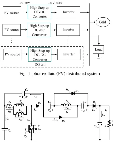
fuel cells, photovoltaic systems, and batteries [3]-[7]. Fig. 1 shows a photovoltaic (PV) distributed
system in which the solar source is low DC input voltage. PV sources can also connect in series to
obtain sufficient DC voltage for generating AC utility voltage; however, it is difficult to realize a
series connection of the PV source without incurring a shadow effect [8], [9]. High step-up DC-DC
converters are generally used as the front-end converters to step from low voltage (12-40 V) up to
high voltage (380-400 V) [10]. High step-up DC-DC converters are required to have a large
conversion ratio, high efficiency, and small volume [11]-[16].
The isolated converters such as forward, flyback, push-pull, half-bridge, and full-bridge types
can adjust the turns ratio of the transformer to achieve high step-up voltage gain. However, the main
switches of these converters will suffer a high voltage spike and high power dissipation from the
leakage inductor of the transformer [17]. To reduce these drawbacks, the non-dissipative snubber
circuits and active-clamp circuits are employed. However, the cost increases accordingly due to the
extra power switch and high side driver [18].
Theoretically, the non-isolated converters can be adopted to provide high step-up voltage gain
with extremely high duty cycle [19]. However, the step-up voltage gain is limited by the effect of
the power switches, rectifier diodes, and equivalent series resistance (ESR) of the inductors and
capacitors. The extreme duty cycle operation may also result in serious reverse-recovery problem
and electromagnetic interference (EMI) problem [20].
To improve the conversion efficiency and achieve high step-up voltage gain, many topologies
have been proposed [19]-[28]. High step-up gain can be achieved by the use of the switched
capacitor technique [22]-[25]. However, the main switch will suffer high transient current, and the
conduction loss is high. Another method for achieving high step-up gain is the use of the
voltage-lift technique [26]-[28]. However, it has the same drawback.
The converters employ the coupled-inductor technique to achieve high step-up gain by
adjusting the turns ratio [29]. However, the leakage inductor of the coupled inductor incurs a
voltage spike on the main switch and affects the conversion efficiency. For this reason, the
converters using the coupled-inductor technique with an active clamp circuit have also been
proposed [30], [31]. An integrated boost-flyback converter is presented, in which the secondary side
of the coupled-inductor is used as a flyback type [32], [33]. The leakage-inductor energy of the
coupled inductor is recycled into the load during the switch-off period, thus the voltage spike on the
main switch can be limited. Additionally, the voltage stress of the main switch can be adjusted by
the turns ratio of the coupled inductor. To achieve high step-up voltage gain, it has been proposed
that the secondary side of the coupled-inductor can be used as a flyback and a forward type
[34]-[36]. Also, several converters that combine output-voltage stacking to increase voltage gain are
proposed [37], [38]. The sepic-flyback converter with the coupled inductor and output stacking
techniques has been proposed [39]. Additionally, a high step-up boost converter that uses multiple
coupled-inductor with output stacking have been proposed [40], [41].
This paper proposes a high efficiency, high step-up voltage gain, and clamp-mode converter.
The proposed converter adds two pairs of additional capacitors and diodes to achieve high step-up
voltage gain. The coupled-inductor is used as both a forward and flyback type, thus the two
capacitors can be charged in parallel and discharged in series via the coupled-inductor. The transit
current does not flow through the main switch compared with earlier studies [22]-[28]. Thus, the
proposed converter has low conduction loss. Additionally, this converter allows significant weight
and volume reduction compared with other converters [29]-[40]. Another benefit is that the voltage
stresses on the main switch and output diode are reduced. However, the leakage inductor of the
coupled-inductor may cause high power loss and voltage spike. Thus, a passive clamping circuit is
needed to recycle the leakage-inductor energy of the coupled inductor and to clamp the voltage
across the main switch. The reverse-recovery problems in the diodes are alleviated, and thus high
efficiency can be achieved.
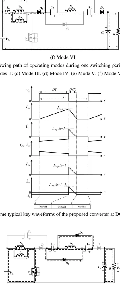
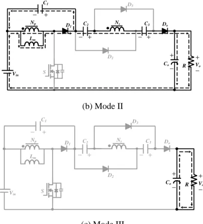
II. O
PERATINGP
RINCIPLE OF THEP
ROPOSEDC
ONVERTERFig. 2 shows the circuit topology of the proposed converter. This converter consists of DC
input voltage V
in, power switch S, coupled-inductor N
pand N
s, one clamp diode D
1, clamp capacitor
C
1, two blocking capacitors C
2and C
3, two blocking diodes D
2and D
3,output diode D
o, and output
capacitor C
o. The coupled inductor is modeled as the magnetizing inductor L
mand leakage inductor
L
k.
To simplify the circuit analysis, the following conditions are assumed:
1) Capacitors C
2, C
3, and C
oare large enough that V
c2, V
c3,and V
oare considered to be constant
in one switching period.
2) The power MOSFET and diodes are treated as ideal, but the parasitic capacitor of the power
switch is considered.
3) The coupling-coefficient of coupled-inductor k is equal to L
m/(L
m+L
k) and the turns ratio of
coupled-inductor n is equal to N
s/N
p.
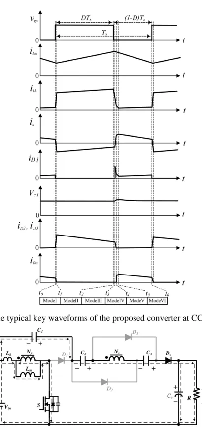
(A) Continuous-Conduction Mode (CCM) Operation
In CCM operation, there are six operating modes in one switching period of the proposed
converter. Fig. 3 shows the typical waveforms and Fig. 4 shows the current-flow path of the
proposed converter for each modes. The operating modes are described as follows:
1) Mode I [t
0, t
1]: During this time interval, S is turned on. Diodes D
1, D
2, and D
3are turned off, and
D
ois turned on. The current-flow path is shown in Fig. 4(a). The primary-side current of the
coupled inductor i
Lkis increased linearly. The magnetizing inductor L
mstores its energy from
DC-source V
in. Due to the leakage inductor L
k, the secondary-side current of the coupled
inductor i
sis decreased linearly. The voltage across the secondary-side winding of the coupled
inductor V
L2, and blocking voltages V
c2and V
c3are connected in series to charge the output
capacitor C
oand to provide the energy to the load R. When the current i
sbecomes zero,
DC-source V
inbegins to charge capacitors C
2and C
3via the coupled inductor. When i
Lkis equal
to i
Lmat t = t
1, this operating mode ends.
2) Mode II [t
1, t
2]: During this time interval, S is still turned on. Diodes D
1and D
oare turned off,
and D
2and D
3are turned on. The current-flow path is shown in Fig. 4(b). The magnetizing
inductor L
mis stored energy from DC-source V
in. Some of the energy from DC-source V
intransfers to the secondary side of the coupled inductor to charge the capacitors C
2and C
3.
Voltages V
c2and V
c3are approximately equal to nV
in. Output capacitor C
oprovides the energy to
load R. This operating mode ends when switch S is turned off at t = t
2.
3) Mode III [t
2, t
3]: During this time interval, S is turned off. Diodes D
1and D
oare turned off, and
D
2and D
3are turned on. The current-flow path is shown in Fig. 4(c). The energies of leakage
inductor L
kand magnetizing inductor L
mare released to the parasitic capacitor C
dsof switch S.
The capacitors, C
2and C
3, are still charged by the DC-source V
invia the coupled inductor. The
output capacitor C
oprovides energy to load R. When the capacitor voltage V
in+V
dsis equal to V
c1at t = t
3, diode D
1conducts and this operating mode ends.
4) Mode IV [t
3, t
4]: During this time interval, S is turned off. Diodes D
1, D
2, and D
3are turned on
and D
ois turned off. The current-flow path is shown in Fig. 4(d). The energies of leakage
inductor L
kand magnetizing inductor L
mare released to the clamp capacitor C
1. Some of the
energy stored in L
mstarts to release to capacitors C
2and C
3in parallel via the coupled inductor
until secondary current i
sequals to zero. Meanwhile, current i
Lkis decreased quickly. Thus,
diodes D
2and D
3are cut off at t = t
4, and this operating mode ends.
5) Mode V [t
4, t
5]: During this time interval, S is turned off. Diodes D
1and D
oare turned on, and D
2and D
3are turned off. The current-flow path is shown in Fig. 4(e). The energy of leakage
inductor L
kand magnetizing inductor L
mare released to the clamp capacitor C
1. The
primary-side and secondary-side windings of the coupled inductor, DC sources V
in, and
capacitors, C
2and C
3, are series to transfer their energies the output capacitor C
oand load R.
This operating mode ends when capacitor C
1starts to discharge at t = t
5.
6) Mode VI [t
5, t
6]: During this time interval, S is still turned off. Diodes D
1and D
oare turned on,
and D
2and D
3are turned off. The current-flow path is shown in Fig. 4(f). The primary-side and
secondary-side windings of the coupled inductor, DC sources V
in, and capacitors, C
1, C
2and C
3,
transfer their energies the output capacitor C
oand load R. This mode ends at t = t
6when S is
turned on at the beginning of the next switching period.
(B) Discontinuous-Conduction Mode (DCM) Operation
In order to simplify the analysis for DCM operation, leakage inductor L
kof the
coupled-inductor is neglected. Fig. 5 shows the typical waveforms when the proposed converter is
operated in DCM, and Fig. 6 shows the current-flow path of the proposed converter for each modes.
There are three modes in DCM operation. The operating modes are described as follows:
1) Mode I [t
0, t
1]: During this time interval, S is turned on. The current-flow path is shown in Fig.
6(a). The part energy of DC-source V
intransfers to magnetizing inductor L
m. Thus, i
Lmis
increased linearly. The DC-source V
inalso transfers another part energy to charge capacitors C
2and C
3via the coupled inductor. The energy of the output capacitor C
ois discharged to load R.
This mode ends when S is turned off at t = t
1.
2) Mode II [t
1, t
2]: During this time interval, S is turned off. The current-flow path is shown in Fig.
6(b). The energy of the magnetizing inductor L
mis released to the capacitor C
1. Similarly,
capacitors C
2and C
3are discharged in a series with DC source V
inand magnetizing inductor L
mto the capacitor C
oand load R. This mode ends when the energy stored in L
mis depleted at t = t
2.
3) Mode III [t
2, t
3]: During this time interval, S remains turned off. The current-flow path is shown
in Fig. 6(c). Since the energy stored in L
mis depleted, the energy stored in C
ois discharged to
load R. This mode ends when S is turned on at t = t
3.
III. S
TEADY-S
TATEA
NALYSIS OF THEP
ROPOSEDC
ONVERTER(A) CCM Operation
At modes IV and V, the energy of the leakage inductor L
kis released to the clamped capacitor
C
1. According to previous work Ref. [15], the duty cycle of the released energy can be expressed as
1 1
2(1 )
1 ,
c c
s
t D
D T n
(1)
where T
sis the switching period, D
c1is the duty ratio of the switch, and t
c1is the time of modes IV
and V.
By applying the voltage-second balance principle on L
m, the voltage across the capacitor C
1can be represented by
1
(1 ) (1 )
1 2 .
c in
D k
V V
D
k n
(2)
Since the time durations of modes I, III, and IV are significantly short, only modes II, V, and
VI are considered in CCM operation for the steady-state analysis.
In the time period of mode II, the following equations can be written based on Fig. 4(b).
1
1
II m ,
L in in
m k
v L V
L L
kV
2 1
(3)
II II .
L L in
2 3 2
c c L in
v nv nkV
(4)
Thus, the voltage across capacitors C
2and C
3can be written as
.
(5)
V V vII nkV
During the time duration of modes V and VI, the following equation can be formulated based on
Fig. 4(f).
2= 2 1 2 3 .
V VI
L L in c c c o
v v V V V V V
(6)
Thus, the voltage across the magnetizing inductor L
mcan be derived as
1 2 3
2 1= 1
VI
V VI L in c c c o
L L
V V V V V
v v v
n n
.
(7)
Using the volt-second balance principle on L
m, the following equation is given
1 1
0 s s 0.
s
DT II T VI
L DT L
v dt v dt
(8)
Substituting (2), (3), (5), and (7) into (8), the voltage gain is obtained as
1 (1
1 1 2 .
CCM
nk D k n
M nk
D D
)( 1)
(9)
The schematic of the voltage-gain versus the duty-ratio under various the coupling coefficients of
the coupled-inductor is shown in Fig. 7. It is seen that the voltage gain is not very sensitive to the
coupling-coefficient. When k is equal to 1, the ideal voltage gain is written as
1
CCM 1
M n n
D
(10)
Fig. 8 shows the voltage gain versus the duty ratio of the proposed converter as compared with
the converters in previous work [35] and [36] at CCM operation under k =1 and n =3. One can see
that the voltage gain of the proposed converter is higher than the converters in [35] and [36].
According to the description of the operating modes, the voltage stresses on the active switch S and diodes D
1, D
2, D
3, and D
oare given as
1 ,
1 1
o in
DS in
V nV
V V
D n
(11)
1
1 ,
1 1
o in
D in
V nV
V V
D n
(12)
2 3 ( )
1 1 .
D D Do in o in
n n
V V V V V nV
D n
1
(13)
Equations (11), (12), and (13) mean that with the same specifications, the voltage stresses on
the main switch and diodes can be adjusted by the turns ratio of the coupled inductor.
(B)DCM Operation
In DCM operation, three modes are discussed. The key waveform is shown in Fig. 5. During
the time of mode I, switch S is turned on. Thus, the following equations can be formulated based on
Fig. 6(a)
I ,
L in
2
v V
(14)
I .
L in
v nV
(15)
The peak value of the magnetizing-inductor current is given as
in .
Lmp s
m
I V DT
L
(16)
Furthermore, the voltage across capacitors C
2and C
3can be written as
2 3 2
c c L in
1 1
.
(17)
V V vI nV
In the time interval of mode II, the following equations can be expressed based on Fig. 6(b):
II ,
L c
2 1 2 3
v V
(18)
II .
L in c c c o
1 2
L L
v V V V V V
(19)
During the time of mode III, the following equation can be derived from Fig. 6(c):
III III 0.
v v
(20)
Applying the voltage-second balance principle on N
p, N
sof the coupled inductor, the following
equations are given as
( )
1 1 1
0 s L s (s 0.
s L s
DT I D D T II T III
L DT L D D T L
v dt v dt v dt
) )
(21)
( )
2 2 2
0 s L s (s 0.
s L s
DT I D D T II T III
L DT L D D T L
v dt v dt v dt
(22)
Substituting (14), (15), (17), (18), (19), and (20) into (21) and (22), the voltage gain is obtained as
follows:
1 ,
c L
V DV
D in
(23)
( 1) (2 1) .
(24)
o in
L
V D n n V
D
According to (24), the duty cycle D
Lcan be derived as
(1 )
(1 2 ) .
in L
o i
D n DV
V n
Vn
(25) From Fig. 5, the average current of i
cois computed as
1 .
2 1
Lmp
co L o
I D I
n
I
(26) Since I
cois equal to zero under steady state, Equations (16), (25), and I
co= 0 into (26) yields
2 2
2 (1 2 ) .
in s o
o in m
D V T V
V n V L
R
(27) Then, the normalized magnetizing-inductor time constant is defined as
m m s,
Lm s
L L f
RT R
(28)
where f
sis the switching frequency.
Substituting (28) into (27), the voltage gain is given by
2 2
1 2 (1 2 )
2 4 2 .
o DCM
in Lm
V n n
M V
D
(29)
The curve of the voltage gain, shown in Fig. 9, illustrates the voltage-gain versus the duty-ratio
under various τ
Lm.
(C) Boundary Operating Condition between CCM and DCM
If the proposed converter is operated in boundary-condition mode (BCM), the voltage gain of
CCM operation is equal to the voltage gain of DCM operation. From (10) and (29), the boundary
normalized magnetizing-inductor time constant, τ
LmB, can be derived as
(1 )2
2(1 )(1 2 ).
LmB
D D
n n nD
(30)
The curve of τ
LmBis plotted in Fig. 10. If τ
Lmis larger than τ
LmB, the proposed converter is operated
in CCM.
IV. D
ESIGN ANDE
XPERIMENT OF THEP
ROPOSEDC
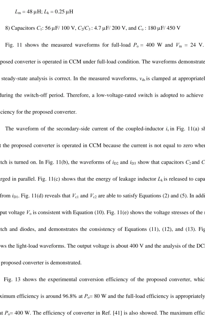
ONVERTERTo verify the performance of the proposed converter, a prototype circuit is implemented in the
laboratory. The specifications are as follows:
1) input DC voltage V
in: 24 V
2) output DC voltage V
o: 400 V
3) maximum output power: 400 W
4) switching frequency: 50 kHz
5) MOSFET S: IRFB4410ZPBF
6) Diodes D
1: SBR20A100CTFP, D
2/D
3: DESI30, and D
o: BYR29
7) Coupled inductor: ETD-59, core pc40, N
p: N
s= 1 : 4
L
m= 48 H; L
k= 0.25 H
8) Capacitors C
1: 56 F/ 100 V, C
2/C
3: 4.7 F/ 200 V, and C
o: 180 F/ 450 V
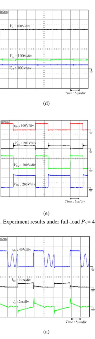
Fig. 11 shows the measured waveforms for full-load P
o= 400 W and V
in= 24 V. The
proposed converter is operated in CCM under full-load condition. The waveforms demonstrate that
the steady-state analysis is correct. In the measured waveforms, v
dsis clamped at appropriately 90
V during the switch-off period. Therefore, a low-voltage-rated switch is adopted to achieve high
efficiency for the proposed converter.
The waveform of the secondary-side current of the coupled-inductor i
sin Fig. 11(a) shows
that the proposed converter is operated in CCM because the current is not equal to zero when the
switch is turned on. In Fig. 11(b), the waveforms of i
D2and i
D3show that capacitors C
2and C
3are
charged in parallel. Fig. 11(c) shows that the energy of leakage inductor L
kis released to capacitor
C
1from i
D1. Fig. 11(d) reveals that V
c1and V
c2are able to satisfy Equations (2) and (5). In addition,
output voltage V
ois consistent with Equation (10). Fig. 11(e) shows the voltage stresses of the main
switch and diodes, and demonstrates the consistency of Equations (11), (12), and (13). Fig. 12
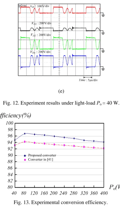
shows the light-load waveforms. The output voltage is about 400 V and the analysis of the DCM of
the proposed converter is demonstrated.
Fig. 13 shows the experimental conversion efficiency of the proposed converter, which the
maximum efficiency is around 96.8% at P
o= 80 W and the full-load efficiency is appropriately 94.2
% at P
o= 400 W. The efficiency of converter in Ref. [41] is also showed. The maximum efficiency
is 94.3% and full-load efficiency is 92.25%. The results show that the proposed converter has
promoted the efficiency about 2%.
The results verify the high efficiency of the proposed converter. Because the low input voltage
is applied in this converter, the proposed converter should experience extremely high input current
at full-load, which would leads to high conduction loss during the switch turn-on period. To further
improving the conduction loss, two of the proposed converter can be used in interleaved operation
where the input current is shared by two switches to achieve high efficiency.
V. C
ONCLUSIONSThis paper proposed a novel, high efficiency and high step-up DC-DC converter. By using the
capacitor charged in parallel and discharged in a series by the coupled-inductor, high step-up
voltage gain and high efficiency are achieved. The steady-state analyses of voltage gain and
boundary operating condition are discussed in detail. A prototype circuit of the proposed converter
is built in the laboratory. Experimental results confirm that high efficiency and high step-up voltage
gain can be achieved. The efficiency is 96.8%. The voltage stress on the main switches is 90 V, thus
low voltage ratings and low on-state resistance levels R
DS(ON)switch can be selected. Moreover, the
proposed converter has simple structure. It is suitable for renewable energy systems in microgrid
applications.
R
EFERENCES[1] Y. Li and Y. W. Li, “Decoupled power control for an inverter based low voltage microgrid in autonomous
operation,” in Proc. IEEE IPEMC, pp. 2490-2496, 2009.
[2] Y. Li, D. M. Vilathgamuwa, and P. H. Loh, “Design, analysis, and real-time testing of a controller for multibus
microgrid system,” IEEE Trans. Power Electron., vol. 19, no. 5, pp. 1195-1204, 2004.
[3] C. L. Chen, Y. W, J. S. Lai, Y.S. Lee, and D. Martin, “Design of parallel inverters for smooth mode transfer
microgrid applications,” IEEE Trans. Power Electron., vol. 25, no. 1, pp. 6-15, Jan. 2010
[4] A. Timbus, M. Liserre, R. Teodorescu, P. Rodriguez, and F. Blaabjerg, “Evaluation of current controllers for
distributed power generation systems,” IEEE Trans. Power Electron., vol. 24, no. 3, pp. 654-664, Mar. 2009.
[5] Y.A.-R.I. Mohamed and E.F. El Saadany, “Hybrid variable-structure control with evolutionary optimum-tuning
algorithm for fast grid-voltage regulation using inverter-based distributed generation,” IEEE Trans. Power Electron.,
vol. 23, no. 3, pp. 1334-1341, May. 2008.
[6] Y.A.-R.I. Mohamed and E.F. El Saadany, “Adaptive decentralized droop controller to preserve power sharing
stability of paralleled inverters in distributed generation microgrids,” IEEE Trans. Power Electron., vol. 23, no. 6,
pp. 2806-2816, Nov. 2008.
[7] Y.W. Li and C.-N. Kao, “An accurate power control strategy for power-electronics-interfaced distributed
generation units operating in a low-voltage multibus microgrid,” IEEE Trans. Power Electron., vol. 24, no. 12, pp.
2977-2988, Dec. 2009.
[8] H. Karimi, A. Yazdani, and R. Iravani, “Negative-sequence current injection for fast islanding detection of a
distributed resource unit,” IEEE Trans. Power Electron., vol. 23, no. 1, pp. 298-307, Jan. 2008.
[9] T. Shimizu, K. Wada, and N. Nakamura, “Flyback-type single-phase utility interactive inverter with power
pulsation decoupling on the dc input for an ac photovoltaic module system,” IEEE Trans. Power Electron., vol. 21,
no. 5, pp. 1264-1272, Sep. 2006.
[10] L. Palma, M. H. Todorovic, and P. Enjeti, “A high gain transformer-less DC-DC converter for fuel-cell
applications,” in Proc. IEEE PESC, pp. 2514-2520, 2005.
[11] P. Biczel, “Power electronic converters in dc microgrid,” in Proc. IEEE CPE Conf., pp. 1-6, 2007.
[12] A.M. Salamah, S.J. Finney, and B.W. Williams, “Single-phase voltage source inverter with a bidirectional
buck–boost stage for harmonic injection and distributed generation,” IEEE Trans. Power Electron., vol. 24, no. 2, pp.
376-387, Feb. 2009.
[13] A. Cid-Pastor, L. MartÕnez-Salamero, C. Alonso, A. El Aroudi, and H. Valderrama-Blavi, “Power distribution
based on gyrators,” IEEE Trans. Power Electron., vol. 24, no. 12, pp. 2907-2909, Dec. 2009.
[14] L. S. Yang, T. J. Liang, and J. F. Chen, “Transformer-less DC-DC converter with high voltage gain,” IEEE Trans.
Ind. Electron., vol. 56, no. 8, pp. 3144-3152, Aug. 2009.
[15] Q. Zhao and F. C. Lee, “High-efficiency, high step-up dc-dc converters,” IEEE Trans. Power Electron., vol. 18,
no. 1, pp. 65-73, Jan. 2003.
[16] R. J. Wai, C. Y. Lin, C. Y. Lin, R. Y. Duan, and Y. R. Chang, “High-efficiency power conversion system for
kilowatt-level stand-alone generation unit with low input voltage,” IEEE Trans. Ind. Electron., vol. 55, no. 10, pp.
3702-3714, Oct. 2008.
[17] N. P. Papanikolaou and E. C. Tatakis, “Active voltage clamp in flyback converters operating in CCM mode
under wide load variation,” IEEE Trans. Ind. Electron., vol. 51, no. 3, pp. 632-640, Jun. 2004.
[18] J. M. Kwon and B. H. Kwon, “High step-up active-clamp converter with input-current doubler and
output-voltage doubler for fuel cell power systems,” IEEE Trans. Power Electron., vol. 24, no. 1, pp. 108-115, Jan.
2009.
[19] B. Axelrod, Y. Berkovich, and A. Ioinovici, “Transformerless DC-DC converters with a very high DC
line-to-load voltage ratio,” Proc. IEEE ISCAS, pp. III435-III438, 2003.
[20] R. J. Wai and R. Y. Duan, “High-efficiency DC/DC converter with high voltage gain,” IEE Proc. Inst. Elect.
Eng.-Electric Power Applications, vol. 152, no.4, pp. 793-802, Jul. 2005.
[21] J.A. Carr, D. Hotz, J.C. Balda, H.A. Mantooth, A. Ong, and A. Agarwal, “Assessing the impact of SiC
MOSFETs on converter interfaces for distributed energy resources,” IEEE Trans. Power Electron., vol. 24, no. 1,
pp. 260-270, Jan. 2009.
[22] Fan Zhang, Lei Du, Fang Zheng Peng, and Zhaoming Qian, “A new design method for high-power high-efficiency
switched-capacitor dc–dc converters,” IEEE Trans. Power Electron., vol. 23, no. 2, pp. 832-840, Mar. 2008.
[23] O. Abutbul, A. Gherlitz, Y. Berkovich, and A. Ioinovici, “Step-up switching-mode converter with high voltage
gain using a switched-capacitor circuit,” IEEE Trans. Circuits and Systems I, vol. 50, no. 8, pp. 1098-1102, Aug.
2003.
[24] B. Axelrod, Y. Berkovich, and A. Ioinovici, “Switched-capacitor/ switched-inductor structures for getting
transformerless hybrid DC-DC PWM converters,” IEEE Trans. Circuits and Systems I, vol. 55, no. 2, pp. 687-696,
Mar. 2008.
[25] B. Axelrod, Y. Berkovich, and A. Ioinovici, “Switched-capapcitor (SC)/Switched-inductor (SL) structures for
getting hybrid step-down CUK/ZETA/SEPIC converters,” in Proc. IEEE ISCAS, pp. 5063-5066, 2006.
[26] F. L. Luo, “Six self-lift DC–DC converters, voltage lift technique,” IEEE Trans. Ind. Electron., vol. 48, no. 6, pp.
1268-1272, Dec. 2001.
[27] F. L. Luo and H. Ye, “Positive output super-lift converters,” IEEE Trans. Power Electron., vol. 18, no. 1, pp.
105-113, Jan. 2003.
[28] F. L. Luo and H. Ye, “Positive output multiple-lift push–pull switched-capacitor Luo-converters,” IEEE Trans. Ind.
Electron., vol. 51, no. 3, pp. 594-602, Jun. 2004.
[29] B. Axelrod, Y. Berkovich, and A. Ioinovici, “Switched coupled-inductor cell for DC-DC converters with very
large conversion ratio,” in Proc. IEEE IECON Conf., pp. 2366-2371, 2006.
[30] B. R. Lin and F. Y. Hsieh, “Soft-switching zeta–flyback converter with a buck–boost type of active clamp,” IEEE
Trans. Ind. Electron., vol. 54, no. 5, pp. 2813-2822, Oct. 2007.
[31] T. F. Wu, Y. S. Lai, J. C. Hung, and Y. M. Chen, “Boost converter with coupled inductors and buck–boost type of
active clamp,” IEEE Trans. Ind. Electron., vol. 55, no. 1, pp. 154-162, Jan. 2008.
[32] K. C. Tseng and T. J. Liang, “Novel high-efficiency step-up converter,” IEE Proc. Inst. Elect. Eng.-Electric Power
Applications, vol. 151, no. 2, pp. 182-190, Mar. 2004.
[33] K. C. Tseng and T. J. Liang, “Analysis of intergrated boost-flyback step-up converter,” IEE Proc. Inst. Elect.
Eng.-Electric Power Applications, vol. 152, no. 2, pp. 217-225, 2005.
[34] R. J. Wai and R. Y. Duan, “High step-up converter with coupled-inductor,” IEEE Trans. Power Electron., vol. 20,
no. 5, pp. 1025-1035, Sep. 2005.
[35] R. J. Wai, L. W. Liu, and R. Y. Duan, “High-efficiency voltage-clamped DC–DC converter with reduced
reverse-recovery current and switch-voltage stress,” IEEE Trans. Ind. Electron., vol. 53, no. 1, pp. 272-280, Feb.
2005.
[36] J. W. Baek, M. H. Ryoo, T. J. Kim, D. W. Yoo, and J. S. Kim, “High boost converter using voltage multiplier,” in
Proc. IEEE IECON, pp. 567-572, 2005.
[37] T. Dumrongkittigule, V. Tarateeraseth, and W. Khan-ngern, “A new integrated inductor balanced switching
technique for common mode EMI reduction in high step-up DC/DC converter,” in Proc. International Zurich
Symposium on Electromagnetic Compatibility, pp. 541-544, 2006
[38] Y. J. A. Alcazar, R. T. Bascope, D. S. de Oliveira, E. H. P. Andrade, and W. G. Cardenas, “High voltage gain
boost converter based on three-state switching cell and voltage multipliers,” in Proc. IEEE IECON, pp. 2346-2352,
2008.
[39] K. B. Park, H. W. Seong, H. S. Kim, G. W. Moon, and M. J. Youn, “Integrated boost-sepic converter for high
step-up applications,” in Proc. Power Electronics Specialists Conf., Rohode, Greece, pp. 944-950, 2008.
[40] G. V. T. Bascope, R. P. T. Bascope, D. S. Oliveira Jr., S. A. Vasconcelos, F. L. M. Antunes, and C. G. C. Branco,
“A high step-up DC-DC converter based on three-state switching cell,” in Proc. IEEE ISIE, pp. 998-1003, 2006.
[41] S. K. Changchien, T. J. Liang, J. F. Chen, L. S. Yang, “Novel high step-up DC-DC converter for fuel cell energy
conversion system,” IEEE Trans. Ind. Electron., vol. 57, no. 6, pp. 2007-2017, 2010.
Fig. 1. photovoltaic (PV) distributed system
Fig. 2. Circuit configure of the proposed converter
Fig. 3. Some typical key waveforms of the proposed converter at CCM operation.
Vo
Vin S Np
D2
Co R Ns
Lk
D3
C2 C3
Lm
Do
C1
D1
(a) Mode I
(b) Mode II
(c) Mode III
(d) Mode IV
Vo
Vin S Np
D2
Co R Ns
Lk
D3
C2 C3
Lm
Do C1
D1
(e) Mode V
(f) Mode VI
Fig. 4. Current flowing path of operating modes during one switching period at CCM operation.
(a) Modes I. (b) Modes II. (c) Mode III. (d) Mode IV. (e) Mode V. (f) Mode VI.
0
i
D2 ,i
D3t
0
0 t
t
DTs DLTs
Ts
i
Lmv
gs0
i
Dot
t0 t1 t2 t3
ModeI ModeII ModeIII
0 t
i
sI
Lmp0
i
cot
ILmp/n+1
-Io
ILmp/n+1
ILmp/n+1 - Io
Fig. 5. Some typical key waveforms of the proposed converter at DCM operation.
Vo
Vin S Np
D2
Co R Ns
D3
C2 C3
Lm
Do
C1
D1
(a) Mode I
Vo
Vin S Np
D2
Co R Ns
D3
C2 C3
Lm
Do
C1
D1
(b) Mode II
Vo Vin S
Np
D2
Co R Ns
D3
C2 C3
Lm
Do C1
D1
(c) Mode III
Fig. 6. Current flowing path of operating modes during one switching period at DCM operation.
(a) Modes I. (b) Mode II. (c) Modes III.
Fig. 7. Voltage-gain versus duty-ratio at CCM operation under n = 3 and various k.
Fig. 8. Voltage-gain versus duty-ratio of the proposed converter, the converters in [35] and [36] at CCM operation under n = 3 and k =1.
Vo / Vin
0 0.1 0.2 0.3 0.4 0.5 0.6 0.7 0.8 0.9 1 0
5 10 15 20 25 30 35 40 45 50
D
DCM (under ٛLm = 0.001) CCM
DCM (under ٛLm = 0.0015) DCM (under ٛLm = 0.002)
Fig. 9. Voltage-gain versus duty-ratio at DCM operation under various τ
Lmand at CCM operation under n = 3 and k = 1.
LmBFig. 10. Boundary condition of the proposed converter under n = 3.
vds: 40V/div
iLk: 20A/div
is: 5A/div
Time : 5 s/div

![Fig. 8. Voltage-gain versus duty-ratio of the proposed converter, the converters in [35] and [36] at CCM operation under n = 3 and k =1](https://thumb-ap.123doks.com/thumbv2/9libinfo/9326117.536370/26.892.213.640.102.1152/fig-voltage-versus-ratio-proposed-converter-converters-operation.webp)