GaN Metal-Semiconductor-Metal Ultraviolet Photodetectors
with Ir/Pt Contact Electrodes
C. L. Yu,aC. H. Chen,bS. J. Chang,a,zand P. C. Changc,
*
aInstitute of Microelectronics and Department of Electrical Engineering, National Cheng Kung University, Tainan 701, Taiwan
b
Department of Electronic Engineering, Cheng Shiu University, Kaohsiung 830, Taiwan c
Department of Electronic Engineering, Nan Jeon Institute of Technology, Yan-Hsui Township, Tainan County 737, Taiwan
Nitride-based ultraviolet metal-semiconductor-metal photodetectors with Ir/Pt and Ni/Au Schottky electrodes were fabricated. It was found that room-temperature effective Schottky barrier height was 0.79 eV for Ir/Pt on GaN. It was also found that we could achieve a 60 times smaller dark current and a 20 times larger photocurrent to dark current contrast ratio by using Ir/Pt contact electrodes. With a 5 V applied bias and an incident light wavelength of 350 nm, it was found that measured responsivity was 0.132 A/W for the detector with Ir/Pt contact electrodes.
© 2006 The Electrochemical Society. 关DOI: 10.1149/1.2402126兴 All rights reserved. Manuscript submitted August 7, 2006; revised manuscript received September 11, 2006. Available electronically December 18, 2006.
In recent years, III-nitride semiconductors have attracted much interest due to their excellent electrical and optical properties. Nitride-based optoelectronic devices, such as light emitting diodes 共LEDs兲1,2
and laser diodes共LDs兲3,4are also commercially available. These materials can also be used as ultraviolet共UV兲 photodetectors 共PDs兲.5
Owing to their wide direct bandgap, superior radiation hard-ness, and high temperature resistance, nitride-based UV PDs are useful in both commercial and military applications. In the last few years, various types of nitride-based UV PDs have been demonstrated.6-9Among them, metal-semiconductor-metal共MSM兲 PDs can be operated with high speed. The fabrication process of MSM PDs is also simple and compatible with field-effect transistor 共FET兲 technology.10
MSM PDs consist of inter-digitated Schottky contacts deposited on top of an active layer. To achieve high-performance MSM UV PDs, it is important to achieve a high Schottky barrier height at the metal-semiconductor interface. A large barrier height leads to small leakage current and high breakdown voltage which could result in improved photocurrent to dark current contrast ratio. To achieve a large Schottky barrier height on GaN, one can choose metals with high work functions, such as Pt 共5.65 eV兲,11
Ni共5.15 eV兲,12and Pd共5.12 eV兲.13However, many of these high work function metals are not stable at high temperatures. In other words, severe inter-diffusion often occurs at the metal-GaN interface when these high work function metals were used.14 Previ-ously, it has been reported that Iridium 共Ir, 5.46 eV兲 could form thermally stable Schottky contact on AlGaN/GaN heterostructure.15 GaN-based UV MSM PDs with IrO2and Schottky diodes with oxi-dized Ir/Ni Schottky contacts were also demonstrated.16,17 Com-pared with Ni, Pt is inert. Ir-Pt alloy is also stable and corrosion resistant. Therefore, in this paper, we report the fabrication of GaN-based UV MSM PDs with Ir/Pt Schottky electrodes. The op-tical and electrical properties of the fabricated PDs will also be discussed.
Experimental
Samples used in this study were all grown on c-face sapphire 共0001兲 substrates by metallorganic chemical vapor deposition 共MOCVD兲.18,19
The samples consisted of a 30 nm thick GaN nucle-ation layer grown at 600°C and a 2m thick undoped GaN layer grown at 1050°C. Room-temperature electron concentration in the samples was⬃1017cm−3. Prior to contact deposition, the samples
were dipped into a diluted hydrochloric acid water solution 共HCl:H2O = 1:1兲 for 5 min to remove native oxide. Ir/Pt
共10 nm/20 nm兲 contact electrodes 共i.e., PD1兲 were subsequently de-posited onto the samples by e-beam evaporation. Standard lithogra-phy and lift-off were then used for the fabrication of MSM PDs. The device consisted of two interdigitated contact electrodes. The finger sizes of the contact electrodes were 14m wide and 100 m long with 6m spacing. The active region of the fabricated PDs was 100⫻ 114 m. For comparison, MSM PDs with conventional Ni/Au共10 nm/20 nm兲 Schottky contacts 共i.e., PD2兲 were also fab-ricated. An HP 4145 semiconductor parameter analyzer was then used to measure current-voltage共I-V兲 characteristics of the fabri-cated PDs both in dark and under illumination. Spectra responses of the detectors were also measured. For spectral responsivity measure-ments, a 250 W Xe lamp and a monochromator were used. The monochromatic light, calibrated with UV-enhanced Si photodetec-tors and an optical power meter, was collimated onto the photode-tectors by using an optical fiber.
Results and Discussion
Figure 1 shows dark I-V characteristics of the MSM PDs mea-sured at various temperatures. It can be seen clearly that dark cur-rents measured from PD1 were smaller than those measured from PD2. With a 10 V applied bias, it was found that room-temperature dark leakage currents of PD1 and PD2 were 2.82⫻ 10−7 and 1.67⫻ 10−5A, respectively. In other words, room-temperature dark
current of PD1 was 60 times smaller than that of PD2. Using simple thermionic emission theory,20 we can determine Schottky barrier heights from these curves. As shown in Table I, it was found that room-temperature effective Schottky barrier heights were 0.79 and
*Electrochemical Society Active Member.
z
E-mail: [email protected]
Figure 1. The dark I-V characteristics of the MSM-PDs with Ir/Pt and Ni/Au as a function of measurement temperature.
Journal of The Electrochemical Society, 154共2兲 J71-J72 共2007兲
0013-4651/2006/154共2兲/J71/2/$20.00 © The Electrochemical Society J71
0.62 eV for the MSM PDs with Ir/Pt and Ni/Au, respectively. The much smaller dark leakage current observed from PD1 could thus be attributed to the larger Schottky barrier height between Ir/Pt and the underneath GaN. It is also possible that the metal-induced gap states 共MIGS兲 was less pronounced on PD1 with Ir/Pt contact.21,22
Previ-ously, it has been shown that the effective Schottky barrier height depends on temperature due to tunneling and other mechanisms.23,24 As shown in Table I, we found that the effective Schottky barrier height decreased by 10.4% for PD1 as we increased the temperature from 25 to 100°C. In contrast, the effective Schottky barrier height decreased by 12.9% for PD2. Such a result suggests that Ir/Pt con-tacts are more suitable for high-temperature applications as com-pared to the conventional Ni/Au contacts.
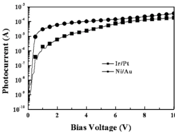
Figure 2 shows photocurrents of the two fabricated MSM PDs. It was found that photocurrent measured from PD2 was slightly larger than that measured from PD1. Photocurrent to dark current contrast ratios can thus be determined from Fig. 1 and 2. With a 5 V applied bias, it was found that photocurrent to dark current contrast ratios were 4.08⫻ 103and 1.78⫻ 102for PD1 and PD2, respectively. In
other words, we could achieve more than 20 times larger photocur-rent to dark curphotocur-rent contrast ratio from the GaN MSM UV PD with Ir/Pt electrodes. Figure 3 shows spectral response of the two fabri-cated MSM PDs. It can be seen clearly that cut-off occurred at around 360 nm for both PDs. With a 5 V applied bias and an inci-dent light wavelength of 350 nm, it was found that measured re-sponsivities were 0.132 and 0.168 A/W for PD1 and PD2, respec-tively. Here, we define UV to visible rejection ratio as the responsivity measured at 350 nm divided by the responsivity mea-sured at 450 nm. With such a definition, we found that UV to visible rejection ratios were 640 and 170, respectively, for PD1 and PD2. Such a result suggests Ir/Pt is potentially useful as the contact ma-terial of nitride-based photodetectors.
Conclusion
GaN-based UV MSM PDs with Ir/Pt and Ni/Au Schottky elec-trodes were fabricated. It was found that room-temperature effective Schottky barrier height was 0.79 eV for Ir/Pt on GaN. It was also found that we could achieve a 60 times smaller dark current and a
20 times larger photocurrent to dark current contrast ratio by using Ir/Pt contact electrodes. With a 5 V applied bias and an incident light wavelength of 350 nm, it was found that measured responsivity was 0.132 A/W for the MSM PD with Ir/Pt contact electrodes.
Acknowledgments
This work was supported by National Science Council under contract no. NSC-91-2215-E-006-012 and NSC-93-2215-E-230-001.
National Cheng Kung University assisted in meeting the publication costs of this article.
References
1. S. Nakamura, N. Senoh, N. Iwasa, and S. Nagahama, Jpn. J. Appl. Phys., Part 2,
34, L797共1995兲.
2. D. S. Wuu, W. K. Wang, W. C. Shih, R. H. Horng, C. E. Lee, W. Y. Lin, and J. S. Fang, IEEE Photon. Technol. Lett., 17, 288共2005兲.
3. S. Nakamura, Semicond. Sci. Technol., 14, R27共1999兲.
4. S. Nakamura and G. Fasol, The Blue Laser Diode, 1st ed., Springer-Verlag, Berlin 共1997兲.
5. M. Razeghi and A. Rogalski, J. Appl. Phys., 79, 7433共1996兲.
6. E. Monroy, E. Munoz, F. J. Sanchez, F. Calle, E. Calleja, B. Beaumont, P. Gibart, J. A. Munoz, and F. Cusso, Semicond. Sci. Technol., 13, 1042共1998兲. 7. E. Monroy, M. Hamilton, D. Walker, P. Kung, F. J. Sanchez, and M. Razeghi, Appl.
Phys. Lett., 74, 1171共1999兲.
8. S. L. Rumyantsev, N. Pala, M. S. Shur, R. Gaska, M. E. Levinshtein, V. Divarahan, J. Yang, G. Simin, and M. A. Khan, Appl. Phys. Lett., 79, 866共2001兲. 9. Y. K. Su, S. J. Chang, C. H. Chen, J. F. Chen, G. C. Chi, J. K. Sheu, W. C. Lai, and
J. M. Tsai, IEEE Sens. J., 2, 366共2002兲.
10. D. L. Rogers, J. Lightwave Technol., 9, 1635共1991兲.
11. S. N. Mohammad, Z. Fan, A. E. Botchkarev, W. Kim, O. Aktas, and A. Salvador,
Electron. Lett., 32, 598共1996兲.
12. J. D. Guo, F. M. Pan, M. S. Feng, R. J. Guo, P. F. Chou, and C. Y. Chang, J. Appl.
Phys., 80, 1623共1996兲.
13. A. C. Schmitz, A. T. Ping, M. A. Khan, Q. Chen, J. W. Yang, and I. Adesida,
Electron. Lett., 32, 1832共1996兲.
14. L. C. Chen, F. R. Chen, J. J. Kai, L. Chang, J. K. Ho, C. S. Jong, C. C. Chiu, C. N. Huang, C. Y. Chen, and K. K. Shih, J. Appl. Phys., 86, 3826共1999兲.
15. C. M. Jeon, H. W. Jang, and J. L. Lee, Appl. Phys. Lett., 82, 391共2003兲. 16. J. K. Kim, H. W. Jang, C. M. Jeon, and J. L. Lee, Appl. Phys. Lett., 81, 4655
共2002兲.
17. H. Jiang, T. Egawa, H. Ishikawa, Y. B. Dou, C. L. Shao, and T. Jimbo, Electron.
Lett., 39, 1604共2003兲.
18. C. H. Chen, S. J. Chang, and Y. K. Su, J. Vac. Sci. Technol. A, 22, 1020共2004兲. 19. S. J. Chang, T. K. Ko, Y. K. Su, Y. Z. Chiou, C. S. Chang, S. C. Shei, J. K. Sheu,
W. C. Lai, Y. C. Lin, W. S. Chen, and C. F. Shen, IEEE Sens. J., 6, 406共2006兲. 20. K. M. Tracy, P. J. Hartlieb, S. Einfeldt, R. F. Davis, E. H. Hurt, and R. J.
Neman-ich, J. Appl. Phys., 94, 3939共2003兲.
21. E. H. Rhoderick and R. H. Williams, Metal-Semiconductor Contacts, 2nd ed., Oxford University Press, New York共1988兲.
22. T. U. Kampen and W. Monch, Appl. Surf. Sci., 117/118, 388共1997兲.
23. L. S. Yu, Q. Z. Liu, Q. J. Xing, D. J. Qiao, and S. S. Lau, J. Appl. Phys., 84, 2099 共1998兲.
24. S. Oyama, T. Hashizume, and H. Hasegawa, Appl. Surf. Sci., 190, 322共2002兲.
Table I. Summary of electrical characteristics as a function of measurement temperature.
25°C 40°C 60°C 80°C 100°C
PD1 0.787 eV 0.774 eV 0.747 eV 0.722 eV 0.705 eV
PD2 0.619 eV 0.587 eV 0.573 eV 0.547 eV 0.539 eV
Figure 2. Measured photocurrents of the MSM-PDs with Ir/Pt and Ni/Au.
Figure 3. The responsivity spectra of the MSM-PDs with Ir/Pt and Ni/Au under 5 V bias.
J72 Journal of The Electrochemical Society, 154共2兲 J71-J72 共2007兲
J72