ZVS-ZCS Bidirectional Full-Bridge DC-DC Converter
Ching-Lung Chu Yi Chen Department of Electrical Engineering
Southern Taiwan University Tainan, TAIWAN. R.O.C. 710
Abstract—A bidirectional zero-voltage-switching (ZVS) and zero- current-switching (ZCS) full-bridge dc-dc converter is proposed in this paper. The proposed full-bridge converter topology with low ripple input current, which converts the energy from battery to DC bus (or load) and vice versa. In order to improve the overall efficiency, the proposed bidirectional converter uses the leakage inductance of the transformer and a capacitor to achieve circuit resonance. The resonant frequency is operated in about double frequencies of the primary switch. In this paper, the main switches and output synchronous rectifiers are operated in ZVS and ZCS when being switched on and switched off. Converter description and operating principles of the proposed converter are discussed in this paper. Finally, a laboratory prototype with output power 250W in both buck/charge operation mode and boost/discharge operation mode is implemented to validate the theoretical analysis.
Keywords- full-bridge DC/DC Converter, ZCS, ZVS, bi- directional Converter.
I. INTRODUCTION
Bidirectional dc-dc converters allow transfer of power between two dc sources, in either direction. There are increasing demands of bidirectional dc-dc converters in applications like dc uninterruptable power supplies (UPS) , battery charger circuits, telecom power supplies, distribution systems and computer power systems[1-8].
The control technology in bi-directional converter utilizes mostly pulse width modulation (PWM) control technology [3- 7]. Because the hard switching PWM technology leads the efficiency of converter can’t increase [9]. In the recent years, the possible implementations of bidirectional converters using soft switching are employed in the technology, such as zero- voltage-switching converters [5, 10-11], series L-L-C resonant converters [12, 13], and parallel resonant converters [14, 15], they can achieve zero-voltage-switching and increase power conversion efficiency. There are shortcomings of variable frequency in quasi-resonant converter (QRC) and multi- resonant converter (MRC) [16, 17], to solve the problems the zero-switching PWM converter is proposed.
This paper proposes a ZVS- ZCS bidirectional full-bridge dc-dc converter for application as fuel cell system, battery charger circuits and distribution systems etc. In order to improve the overall efficiency, decrease the circuit complexity and have a simple control circuit, it can be implemented in the proposed topology. The leakage inductance of the transformer and a capacitor are utilized to achieve circuit resonance. The proposed ZVS-ZCS bidirectional full-bridge dc-dc converter
can achieve both small ripple of the input current and small ripple of the output voltage. Furthermore, the main switches and output synchronous rectifiers are operated in ZVS and ZCS when being switched on and switched off.
Vin 1
Lin
1
Cr
Q1
Q2
Q3
Q4
1
Qa Qa3
2
Qa Qa4
Vbatt
io 1
CS
1
DS
2
CS
2
DS
3
CSDS3
4
CS
4
DS
1
CSa
1
DSa
2
CSa
2
DSa
4
CSa
4
DSa 3
CSa
3
DSa 1
vds
2
vds
1
vdsa
2
vdsa
2
Cr 2
Lin
NpNs Llkp Llks ip
im
is
Iin 1
icr 1
vcr
vp vs
ibatt 2
vcr
2
icr
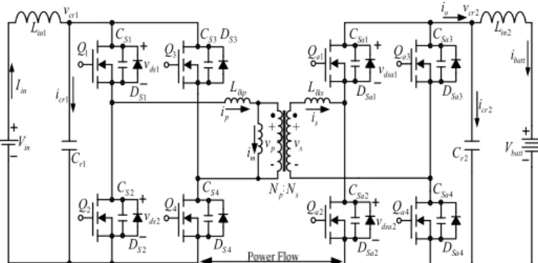
Fig. 1 Proposed ZVS-ZCS Bidirectional Full-Bridge DC-DC Converter.
II. CONVERTER DESCRIPTION
The power stage diagram of the proposed ZVS-ZCS bidirectional full-bridge dc-dc converter is shown in Fig. 1.
The converter has two modes of operation. When power flows from the low voltage side to the high voltage side, the circuit works in discharge operation (boost mode) to power the high voltage side load; otherwise, it works in charge operation (buck mode) to charge the low voltage side battery.
In the buck / charge operation mode, the energy from the dc mains charges the battery. It consists of MOSFET main switchesQ1~ Q4, input inductorL , resonant capacitorin1 C . r1
The shunt capacitors Cs1~Cs4 and the shunt body diodes
4
1~ s
s D
D are the parasitic drain-to-source capacitance and body diode of the MOSFET, respectively. The series inductor
Llkp is the leakage inductor of the main side of the transformer. The series inductor Llks is the leakage inductor of the secondary side of the transformer. The parameter values of the transformer are measured by a LCR meter, and the equivalent leakage inductor is calculated by (1).
⎥⎥
⎦
⎤
⎢⎢
⎣
⎡ ⎟⎟⎠ ×
⎜⎜ ⎞
⎝ +⎛
= lks
S P lkp
r L
N L N L
2 (1)
In the boost/discharge operation mode, the switchesQa1~Qa4are as main switches. The shunt capacitors
4 1~ sa
sa C
C and the shunt body diodes Dsa1~Dsa4 are the parasitic drain-to-source capacitance and body diode of the MOSFET respectively. Switches Q1~ Q4 are the output synchronous rectifiers.
1.83 : 1
Np
:
NsLlkp Llks
u
Lp 137.5 Ls 462.2u ip
im
Fig. 2 Transformer model
In the charge/discharge mode, utilizing the magnetizing current of the transformer and the parasitic drain-to-source capacitors, the voltage of main switches will fall to zero before the main switches are turned on. Therefore, the main switches can be operated under ZVS. When the switches are turned off, a resonant circuit is formed through the equivalent leakage- inductance and the resonant capacitor. Thus, both the main switches and the output rectifier can be operated under ZCS.
The overall efficiency of the converter will increase.
III. DescriptionofOperatingPrinciple
The gate signal of the ZVS-ZCS bidirectional full-bridge dc-dc converter is symmetric switching. Before the main switches are turned on, the switches voltage is discharged to zero, it can make the main switches turn-on under ZVS. At the same time, the resonant circuit is composed of the resonant capacitor and the resonant inductor, the current of the circuit is activated in a sinusoidal waveform that is raised from zero and falls to zero. Therefore, before the switch is turned off and the current falls to zero, both the main switches can be operated under ZCS.
The following assumptions are made to simplify the analysis of the proposed ZVS-ZCS bidirectional full-bridge dc-dc converter.
1. Input suppressed inductanceLin1, Lin2is large, therefore, the input current ripple is small.
2. The inductors and capacitors are ideal, series equivalent resistance doesn’t be considered.
3. Output capacitances are large enough, so can be considered as voltage sources.
Vin
Q1
Q2
Q3
Q4
1
Qa Qa3
2
Qa Qa4
Vbatt
io 1
CSDS1
2
CS
2
DS
3
CSDS3
4
CS
4
DS
1
CSaDSa1
2
CSa
2
DSa
4
CSa
4
DSa 3
CSa
3
DSa 1
vds
2
vds
1
vdsa
2
vdsa 1
ids ids3
2
ids ids4
1
Lin
1
Cr Cr2
2
Lin
3
idsa 3
vds
4
vds
2
idsa Llkp Llks ip
im
is
vp vs
NpNs
Iin 1
vcr
1
icr
2
vcr
2
icr ibatt
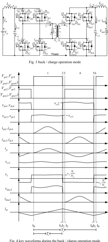
Fig. 3 buck / charge operation mode 2
1 3 4 56
t0 t1t2t3 t4t5t6
Ts
Tr
) , (
,
4 1
4 1
gsa gsa
gs gs
V V
V V
) , (
,
3 2
3 2
gsa gsa
gs gs
V V
V V
4 1, ds
ds v v
3 2, ds
ds v v
4 1,ds
ds i i
3 2,ds
ds i i
ip
1
vcr
vs
2
vdsa
2
idsa
im
1
vcr
p s pN v N 1
vcr
p s
pN
v N
Fig. 4 key waveforms during the buck / charge operation mode
A. Buck / charge operation mode
In this mode, Fig. 3, the dc mainsVin, powering the load, provides the battery charging currentio. Fig. 4 depicts the key waveforms of the proposed ZVS-ZCS bidirectional full-bridge dc-dc converter that is operated in buck / charging mode. Fig.
5 shows the six stages occur over one switching cycle in the
Vin
Q1
Q2
Q3
Q4
1
Qa Qa3
2
Qa Qa4
Vbatt
io S1
C
2
CS
3
CS
4
CS
1
CSa
2
CSa CSa4
3
CSa 1
vds
2
vds
1
vdsa
2
vdsa 1
ids ids3
2
ids ids4
1
Lin
1
Cr Cr2
2
Lin 1
idsa 3
vds
4
vds
4
idsa
Llkp
Llks
ip
im
is
vp vs
NpNs Iin
1
vcr
1
icr
2
vcr
2
icr
ibatt
Vin
Q1
Q2
Q3
Q4
a1
Q 3
Qa
a2
Q Qa4
Vbatt
io S1
C
S2
D
S3
D
S4
C
Sa1
C
2
DSa
4
CSa 3
DSa 1
vds vdsa1
1
ids ids3
2
ids ids4 1
Lin
1
Cr Cr2
2
Lin 1
idsa
4
vds
4
idsa
Llkp
Llks
ip
im
is
vp vs
NpNs
Iin 1
vcr
1
icr
2
vcr
2
icr
ibatt
Vin
Q1
Q2
Q3
Q4
1
Qa Qa3
2
Qa Qa4
Vbatt
io 1
CS
2
CS
3
CS
4
CS
1
CSa
2
CSa CSa4 3
CSa 1
vds
2
vds
1
vdsa
2
vdsa 1
ids ids3
2
ids ids4 1
Lin
1
Cr Cr2
2
Lin
3
idsa 3
vds
4
vds
2
idsa
Llkp Llks ip
im
is
vp vs
NpNs
Iin 1
vcr
1
icr
2
vcr
2
icr
ibatt
Vin
Q1
Q2
Q3
Q4
1
Qa
3
Qa
2
Qa Qa4
Vbatt
io 1
DS
2
CS
3
CS
4
DS
1
DSa
2
CSa
4
DSa 3
CSa
2
vds vdsa2
1
ids ids3
2
ids ids4 1
Lin
1
Cr Cr2
2
Lin
3
idsa 3
vds
2
idsa
Llkp Llks ip
im
is
vp vs
NpNs
Iin 1
vcr
1
icr
2
vcr
2
icr
ibatt
Vin
Q1
Q4
1
Qa
4
Qa
Vbatt
io
2
CS
3
CS
2
CSa
3
CSa
2
vds ds1
i ids3
ds2
i ids4
in1
L
r1
C Cr2
in2
L
dsa1
i
ds3
v
dsa4
i Llkp Llks
ip
im
is
vp vs
NpNs
Iin cr1
v
cr1
i
cr2
v
cr2
i ibatt
Q3
Q2
3
Qa
2
Qa
Vin
Q1
Q2
Q3
Q4
1
Qa Qa3
2
Qa Qa4
Vbatt
io 1
CS
4
CS
1
CSa
4
CSa 1
vds vdsa1
1
ids ids3
2
ids ids4
1
Lin
1
Cr Cr2
2
Lin
3
idsa
2
idsa
Llkp
Llks
ip
im
is
vp vs
NpNs Iin
1
vcr
1
icr
2
vcr
2
icr
ibatt
4
vds
Fig. 5 Equivalent circuits of the proposed converter in buck / charging mode:
(a) stage1
[
t0≤t≤t1]
, (b) stage2[
t1≤t≤t2]
, (c) stage3[
t2≤t≤t3]
,(d) stage4[
t3≤t≤t4]
, (e) stage5[
t4 ≤t≤t5]
, (f) stage6[
t5≤t≤t6]
.steady state operation in charge operation (buck mode).
Stage 1:
[
t0≤t≤t1]
At t=t0−, the parasitic capacitor voltage of main switch Q1 and Q4 are completely discharged and vds1(t) and
)
4(t
vds decreases to zero.Q1andQ4 are then turned on, as shown in Fig. 5(a), and operated under ZVS. At the same time, the parasitic capacitor voltage vds1(t) and vds4(t)of the main switch Q2andQ3 was approximately charged tovcr1. The input current Iin continues to charge the resonant capacitorCr1, and the resonant inductor current ip(t) forms a parallel LC resonant circuit loop through the equivalent leakage-inductance of the transformer. The resonant inductor current )ip(t is in a sinusoidal waveform and falls to zero at
t1
t= , which causes the main switch Q1andQ4to be turned off along with ZCS. When the gate signal is removed at t=t1,
this stage is finished. In this state, the resonant inductor current )ip(t includes the magnetizing currentim(t), which is
very small compared with the resonant current. To simplify this circuit for analysis, the magnetizing current is neglected in this stage. The equivalent resonant circuit is shown in Fig.
5(a). The resonant inductor currentip(s), resonant capacitor voltage vcr1(s) , resonant capacitor current icr1(s) , can be written as:
( ) ( ) ( )
( )
( )
[ ]
( )
( ) ( ) ( )( )
[ ]
( )
(
inr r r o inr r ino r inr o r r o in r o)
o in Lo o Lr r Lin in
o r in o r r o r in r o in r r in o r r r in
cr cr r in r o o cr r in cr in o r
o r in o r r o r in r o in r r in o r r r in
Lr r r in r o Lo o r in L in r o
o r in o r r o r in r o in r r in o r r r in
cr cr r o r in Lr r r o r in p
L L L L C L s L C L s C L L s L C L s L C L C L s s
s V i V L i L i L
L L L L C L s L C L s C L L s L C L s L C L C L s s
s V V C L C L V V C L V V L C
L L L L C L s L C L s C L L s L C L s L C L C L s s
s i L C L C L i L C L i L C L
L L L L C L s L C L s C L L s L C L s L C L C L s s
s V V C L C L s i L C L C s L
i
+ + + + + + +
+ − + + +
+ + + + + + +
+
− + +
− + + −
+ + + + + + +
+ + + +
+ + + + + + +
+
−
= +
0 2 1 2 0 2 1 2 0 1 4
0 2 1 2 0 2 1 2 0 1 4
1 0 1 0 0
1 1 0
0 2 1 2 0 2 1 2 0 1 4
2 1 0 1 0
0 2 1 2 0 2 1 2 0 1 4
3 1 0 0 1 4 0 1
(2)
( ) ( ) ( )
s i s i sicr1 = in − p (3)
( ) ( ) ( )
s V s sC
i s
v cr
r cr cr
0
1 1
1 1
1 = ⋅ + (4)
Stage 2
[
t1≤t≤t2]
At the beginning of this stage, the resonant circuit is finished and only the magnetizing current remains in the circuit. The equivalent circuit is shown in Fig. 5(b). At the same time, the main switch Q and1 Q are turned off, and the 4 main switch Q and2 Q are not turned on. Subsequently, the 3 magnetizing current im(t) charges the parasitic capacitor
1
C and s C , Thus, the parasitic capacitor s4 C and s2 C voltage s3
)
2(t
vds and vds3(t) is reduced to zero, and the parasitic diode D ands2 D become forward-biased. The parasitic s3
capacitor C and s1 C voltage s4 vds1(t) and vds1(t) are increased tovcr1(t), and this stage finishes. In this state, the equations of the parasitic capacitor C and s1 C changes and s4 C and s2 C s3
discharges can be written as:
⎪⎪
⎪⎪
⎪
⎩
⎪⎪
⎪⎪
⎪
⎨
⎧
=
−
=
−
=
=
∫
∫
∫
∫
2 1 1 4
2 3 1 1 3
2 2 1 1 2
2 1 1 1
1 ) (
1 ) ( ) (
1 ) ( ) (
1 ) (
t
t m
s ds
t
t m
s r c ds
t
t m
s r c ds
t
t m
s ds
dt C I
t V
dt C I
t v t V
dt C I
t v t V
dt C I
t V
(11)
Stage 3
[
t2≤t≤t3]
The magnetizing current im(t) passes through the parasitic diodeD and s2 D , while the main windings3 N and resonant p
capacitor form a circuit loop. The equivalent circuit is shown in Fig. 5(c). At the same time, the input current I charges in
the resonant capacitorC , and the resonant capacitor voltage r1
)
1(t
vcr increases linearly. The vp(t) voltage is nearly equal to )
1(t
vcr and increases linearly. When vs(t2)≤Vbatt and Q , a2 3
Q is not turned on, and the a vds1(t2) is equal to vds4(t2). The secondary side voltage vs(t2)of the transformer can be written as:
) ( )
(2 v 1 t2 N t N
v cr
p s
s = (12)
The models of stage 4
[
t3≤t≤t4]
, stage 5[
t4≤t≤t5]
and stage 6[
t5≤t≤t6]
are similar to the models of stage 1, 2, and 3, respectively. Therefore, the explanations are omitted in this paper.B. Boost / discharge operation mode
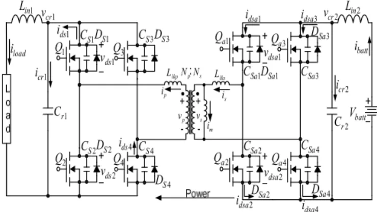
The converter operates in this mode, Fig. 6, on failure of the dc mains. The battery discharges to supply the load power.
The drive method of the switch and the operation mode of the converter in the circuit are the same as buck / charge operation mode, so we don’t discuss here.
Q1
Q2
Q3
Q4
1
Qa Qa3
2
Qa Qa4
Vbatt 1
CSDS1
2
CS DS2 3
CS DS3
4
CS
4
DS
1
CSaDSa1
2
CSa
2
DSa
4
CSa
4
DSa 3
CSa 3
DSa 1
vds
2
vds
1
vdsa
2
vdsa 1
ids
4
ids 1
Lin
1
Cr
2
Cr 2
Lin 1
idsa idsa3
2
idsa
4
idsa
ibatt 2
vcr
2
icr
iload 1
icr 1
vcr
Llkp Llks ip
im
is
vp vs NpNs
Fig. 6 boost / discharge operation mode
IV. Experimental results
In order to verify the proposed ZVS-ZCS bidirectional full-bridge dc-dc converter theoretical analysis, a 250W output power charge mode (buck mode) and a 250W output power discharge mode (boost mode) will be built and tested in the laboratory. The configuration of the proposed converter is shown in Fig 1. The experimental results are obtained with the following parameters as table 1:
Table 1 Experimental parameters
A. Buck/charge operation mode
The experimental results in charging mode at full load are shown in Fig. 7 to Fig. 9. Fig. 7 shows the waveforms of the drain-to-source voltages v and the switch current ds1 i of ds1
power MOSFET Q at the full load. It is observed that, before 1 current i starting to rise from zero, the drain-to-source ds1
voltage v is also zero. Thus, the main switches ds1 Q ~1 Q are 4 turned on under ZVS. Due to a greater equivalent induction leakage of the transformer, the switches current can’t fall to zero, as shown in fig. 7.
Fig. 8 shows the waveforms of the output synchronous rectification switches voltage vdsa1 and the current idsa1 at the full load, where the switch current idsa1 starts to rise from zero.
As shown, the output synchronous rectifiers are turned on by ZVS.
Input DC voltage
Output DC voltage
Output Power
Resonant equivalent
inductor
Resonant capacitor Buck/Charge
mode
5 . 56
~ 4 .
45 24.6~28.3 250W 1.004μH 10μF
Boost/Discharge mode
2 . 25
~ 3 .
24 39.3~46.3 250W 0.42μH 11μF
Fig. 9 shows the waveforms of the dc source input current i , resonant current of transformer in i , and resonant capacitor p
voltage v at the full load. The proposed converter can cr1
achieve a steady state and small ripple input current i in without adding any extra filter.
The efficiency of proposed converter in charging mode is shown in Fig. 10. The proposed converter has the maximum efficiency of 89% at full load condition from 50 W to 250 W.
1
ids 1
vgs
1
vds
div V
vgs1=10 / , vds1=50V/div, ids1=10A/div, div
s μ time=10 /
Fig. 7 Experimental waveforms of the ZVS-ZCS for Q1 at the full load.
1
vdsa
1
idsa
div V
vdsa1=20 / , idsa1=10A/div, time=10μs/div Fig. 8 ZCS operations for output synchronous rectifiersQa1at the full load.
1
vcr
ip
iin
div V
vcr1=40 / , iin=2A/div, ip=5A/div, time=10μs/div Fig. 9 Waveforms of vcr1,
i
in, and ip at the full load.Fig. 10 measured efficiency at different load levels at charging mode B. Boost/discharge operation mode
The experimental results in discharging mode at full load are shown in Fig. 11 to Fig. 13. Fig. 11 shows the turned-on transient waveforms ofQ includinga1 vgsa1,vdsa1andidsa1,and we confirmed that Q is turned-on in ZVS condition. The drain-a1
source voltage vdsa1 and drain current idsa1 of MOSFET Q at a1
the full load are shown in Fig.11, as shown, when the drain current idsa1 of switch decreases to zero, the drain-source voltage vdsa1 is turned on. Thus, the main switches Q ~a1 Q a4 are turned on under ZVS. Due to a greater equivalent induction leakage of the transformer, the switches current can’t fall to zero, as shown in fig. 11.
Fig. 12 shows the waveforms of the output synchronous rectification switches voltage v and the current ds1 i at the ds1
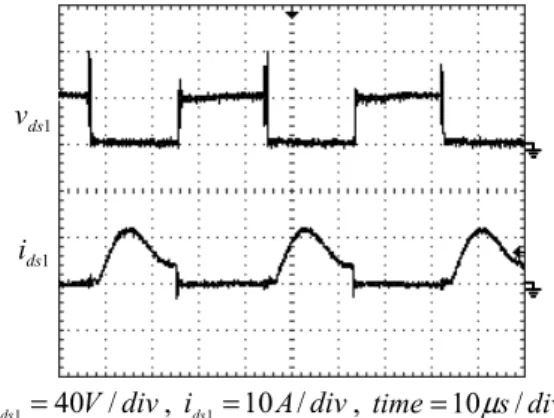
full load, where current i starts to rise from zero. As shown, ds1 the output synchronous rectifiers are turned on by ZVS.
Fig.13 shows the waveforms of the battery currenti , batt
resonant current of transformeri , and resonant capacitor s voltage vcr2 at the full load. The proposed converter can achieve a steady state and small ripple input current i batt without adding any extra filter.
The efficiency of proposed converter in discharging mode is shown in Fig. 14. The proposed converter has the maximum efficiency of 86% at full load condition from 50 W to 250 W.
1
vgsa
1
vdsa
1
idsa
div V
vgsa1=10 / ,vdsa1=50V/div,idsa1=20A/div, div
s time=10μ /
Fig. 11 Experimental waveforms of the ZVS-ZCS forQa1at the full load.
buck/charge mode of efficiency(η)
82%
84%
86%
88%
90%
92%
94%
96%
98%
100%
0 50 100 150 200 250 300
Power (W) η (%)
Duty = 45.4%