國立臺灣大學電機資訊學院光電工程學研究所 碩士論文
Graduate Institute of Photonics and Optoelectronics College of Electrical Engineering and Computer Science
National Taiwan University Master Thesis
於玻璃基板與塑膠基板上製作 高效能氧化鋅薄膜電晶體
High Performance ZnO Thin Film Transistors on Both Glass and Plastic Substrates
研究生﹕劉建承 Liu, Chien Cheng 指導教授﹕黃建璋 博士
中華民國 九十六 年 七 月
July 2007
i
謝 誌
今年早春特地赴會椰林大道上的杜鵑花季,她們仍然開得那麼理直氣壯,頗 有「乃校」之風;荏苒光陰,幾場梅子雨,幾件羽毛衣,回首兩年多在台大的研究 生涯,也曾經如此理直氣壯,漸漸,卻也學會真正用心傾聽。
由衷感謝指導老師黃建璋博士在學術研究上的悉心引導,不僅在研究主題上 給予精闢的指導及見解,也讓我有機會參與資策會無線網路感測的計畫,從中學 習到天線傳播的相關理論;另外,在協助帶領大學部光電實驗的電光調變器實驗 中,也學到不少有趣的應用,這趟碩士班的學涯,收穫良多。也感謝口試委員陳 奕君教授以及陳敏璋教授不吝指教,而讓這本論文更具完整性。
由衷感謝 402 實驗室的所有夥伴們。和育昇一起分享討論實驗、製程、原理 以及女人,挑燈夜戰馬力歐賽車為的是那些令人又愛又恨的 data;和下巴、子樸、
子揚、志豪共度豬羊變色的那些夜晚;和成熟穩重的旻諺哥以及倜儻瀟灑萬人迷 小銘討論深奧的物理;兩位博班學長正彬哥、柯董真是實驗室活力的泉源;還有 可愛的學弟們孟倫、振印、弘憲、兩儀、原禎,光中、世驊、小潘、宏禮,你們 讓 402 充滿了無盡的歡笑。
由衷感謝方瑜老師,弭平了我左腦和右腦的齟齬,讓我的生活不致分裂而得 以發展更完整的性靈。或快或慢,或理性或感性,或邏輯或用情...;學會用我的 兩種步伐,陪著我平穩前進。學會不偏廢任一種心智,隨心所欲,隨緣立善,「妻 子」和「情人」一樣,都得用力珍惜。
也感謝在台北求學階段一路相伴的所有好朋友:口條清晰報新聞的專家「查爾 頓」,適合當聊天系藝人的「大柔」學妹,走音救星吉他手「小綿羊」,十年深厚交情 小吃攤正妹「花枝」和「米粉」,遠在溫哥華的重量級笑話高手「鄧弻」,聊心事的話 匣子「痞堅」,未來的大作家「志摩」弟,大學麻吉「國勳」、「家豪」、「譽達」、「奕寰
」...,族繁不及備載;和你們一起朝馳江皐,夕濟西澨,上山下海,放任我們的 年少輕狂於歌聲笑語中,我們一起拼湊的燦爛時光,都將積澱在我的漫漫長夜裡。
最大的感謝要獻給老爸、老媽,你們無怨悔的支持以及全然的信任,使我可 以安心地去實踐我的志願及夢想;夜闌人靜時,憶起老爸的千萬交代「要活得快樂
」,竊想有這麼開明的父母親,人生就足以快活了。小時候住在家裡面,長大了之 後,我的家,反而住進了我裡面,如影隨形。
漫步在曲徑通幽的舟山路上,兩岸景色依舊青山,依舊夕陽,許多的回憶在 這美麗的台大校園裡,終不散;許多的感恩在我的心中,雖不見。滿載而歸的六 年歲月,僅以數筆,略表心意,不盡之情,就拈花微笑吧。
2007 年 7 月 25 日於台北長興街
ii
Abstract
This thesis focuses on two aspects of ZnO thin film transistors, the ZnO-TFTs fabricated on glass substrates and the flexible ZnO-TFTs fabricated on polymer substrates.
The first part demonstrates a high-performance enhancement-mode ZnO TFT on a glass substrate. Before realizing the TFT device, the characteristics of ZnO thin films are examined to find out the optimal deposition conditions. The ZnO thin film is deposited by RF magnetron sputtering with the presence of O2 at low deposition rate and low temperature. The IDS of the ZnO-TFT on glass substrates is as high as 1 mA when biased at the saturation region VDS = 10-20 V and VGS = 5 V without any post thermal anneal. The Ion/Ioff ratio is 3106. We believe the results are among the best ZnO TFTs ever obtained.
The second part focuses on the flexible ZnO-TFT on PET (polyethylene terephthalate) substrates. All the patterns are defined by standard photolithography with only two steps in order to reduce the distortion of PET substrates. The ZnO thin film is deposited by RF magnetron sputtering at low temperature in presence of O2. The gas flow ratio of Ar to O2 is based on the optimal conditions obtained in the case of the ZnO-TFTs on glass substrates. Titanium is also employed in substitution for ITO as the source and the drain layers to improve the electrical performance. The IDS–VDS curves along with optical transmission of the whole TFT are presented.
iii
摘 要
本論文研究製作於玻璃基板與塑膠基板上之氧化鋅薄膜電晶體的 特性。
在實現薄膜電晶體元件之前,本文首先探討氧缺陷對氧化鋅薄膜
導電特性的影響,藉由濺鍍沉積氧化鋅薄膜時控制 Ar 和 O2的比例,
以及利用氧電漿對氧化鋅薄膜表面進行處理,以獲得最佳製備氧化鋅 薄膜的成長環境。根據此最佳化條件,本研究在玻璃基板上製作出高
效能增強型氧化鋅薄膜電晶體,在 VDS=10–20,VGS=5V 的偏壓下,操
作電流可高達 1mA,開關電流比可達3106,是目前氧化鋅薄膜電晶體
的研究工作中,效能表現最好之一。
本文進一步探討製作於塑膠基板上之氧化鋅薄膜電晶體的特性。
採用兩步驟的黃光製程,以防止塑膠基板在化學溶劑中產生變形;而 受限於塑膠基板的玻璃轉換溫度,所有薄膜均在室溫下濺鍍成長,氧 化鋅的成長條件是利用玻璃基板上的最佳結果。另外,採用金屬鈦作 為汲極和源極,以改善接觸電阻。塑膠基板上之氧化鋅薄膜電晶體的 電特性曲線和可見光穿透率均本文中亦有論及。
iv
Table of Contents
謝誌 Abstract 摘要
page
Chapter 1 Introduction... 1
Chapter 1 Bibliography……….. 5
Chapter 2 Literature Review and Theory... 6
2.1 Transistors……….………….. 6
2.1.1 Working principle of field effect transistors... 6
2.1.2 Operation of thin film transistors... 13
2.1.3 Si-based thin film transistors... 17
2.1.4 Oxide-semiconductor-based thin film transistors... 21
2.1.5 Flexible thin film transistors... 23
2.2 Property of Materials... 26
2.2.1 Zinc oxide (ZnO)... 26
2.2.2 Indium tin oxide (ITO)... 33
2.2.3 Insulating materials... 35
2.3 Property of Substrates... 36
2.3.1 Glass substrate... 36
2.3.2 Polymer substrates... 39
2.4 Plasma Reaction and Sputtering... 44
Chapter 2 Bibliography... 47
v
page
Chapter 3 Fabrication of ZnO TFTs on a Glass Substrate... 52
3.1 Fabrication Process... 52
3.2 Results and Analysis... 55
3.2.1 Quality of ZnO thin films... 55
3.2.2 Performance of the ZnO-TFTs... 67
3.2.3 Performance of the best ZnO-TFT... 79
Chapter 4 Fabrication of ZnO TFTs on Plastic Substrates... 83
4.1 Fabrication Process... 83
4.2 Results and Analysis... 86
4.2.1 Using ITO as the source and drain... 86
4.2.2 Using Ti as the source and drain... 89
Chapter 5 Conclusions and Recommendations for Future Work.. 91
5.1 Conclusions... 91
5.2 Recommendations for Future Work... 93
vi
List of Figures
Figure page 1.1 The display application of flexible electronics. (a) Fujitsu
e-paper. (b) An e-paper newspaper. (c) E-papers look like real
sheets of paper. (d) A foldable display... 4 2.1 FETs: (a) n-channel FET; (b) p-channel FET... 7 2.2 Structure of NMOS... 7 2.3 The depletion region and the channel at different gate bias. (a)
VG=0, (b) VG<Vth, (c) VG= Vth, (d) VG>Vth... 8~9 2.4 Output characteristics when VDS is quite small... 9 2.5 Variation of channel and depletion region at a constant VG
when (a) VDS < VDsat; (b) VDS = VDsat; (c) VDS > VDsat... 11 2.6 Output characteristics... 11 2.7 (a) The cross-section of a MOS capacitor and corresponding
energy band diagrams for several biasing conditions: (b) equilibrium, (c) accumulation (VGS > 0 V), and (d) inversion
(VGS < 0 V)... 14 2.8 An n-channel accumulation-mode TFT operating in (a)
pre-pinch-off and (b) post-pinch-off regime... 15 2.9 Structure of an a-Si TFT and in the inset, the flowchart
outlines the processes for making an a-Si TFT array using a bottom-gate TFT structure and an independent storage
capacitor... 17 2.10 Cross-sectional view of a (a) MOSFET and (b) TFT... 18 2.11 Four thin-film transistor configurations: (a) staggered
bottom-gate, (b) coplanar bottom-gate, (c) staggered
top-gate, and (d) coplanar top-gate... 20 2.12 Material properties of IGZO system. Room temperature Hall
mobility and carrier concentration as functions of chemical composition. Values outside and inside parentheses show Hall mobility in cm2/Vs and carrier concentration in 1018 cm-3, respectively... 24
vii
2.13 Crystal structure of wurtzite ZnO... 28 2.14 Energy levels of native defects in ZnO. The donor defects are
2
Zni , Zni, Zni,VO2,VO,VOand the acceptor defects areVZn'',
VZn'... 28 2.15 A simplified section of the unit cell of In2O3 (ITO, as well).
The distance between the oxygen atoms varies between 2.8
and 2.9 Å ... 34 2.16 Comparison of a range of plastics by glass transition... 39 2.17 Surface roughness of (a) Teonex Q83 and (b) Teonex Q65,
films produced by DuPont... 43 2.18 The process of Ar plasma generation... 45 2.19 Magnetron sputtering... 46 3.1 The structure of the ZnO-TFT on a glass substrate. (a) A
schematic cross-sectional view of TFT structure. (b) A
perspective from top view... 52 3.2 (a) ~ (g) The flowchart of fabrication process of ZnO-TFTs
on a glass substrate... 54 3.3 XRD data of ZNO-A, ZNO-B and ZNO-C... 56 3.4 AFM images of (a) ZNO-A, (b) ZNO-B and (c) ZNO-C... 57 3.5 I-V curves of the TFTs with (a) ZNO-A, (b) ZNO-B, and (c)
ZNO-C as channel layers, respectively... 58~59 3.6 XRD data of ZNO-P, ZNO-Q, ZNO-R, and ZNO-S... 61 3.7 Resistivity of ZNO-P, ZNO-Q, ZNO-R, and ZNO-S... 62 3.8 AFM images of (a) ZNO-P, (b) ZNO-Q, (c) ZNO-R, and (d)
ZNO-S... 62~63 3.9 I-V curves of the TFTs (a) TFT-P, (b) TFT-Q, (c) TFT-R, and
(d) TFT-S. For TFT-P and TFT-R, the transfer curves are
included... 64 3.10 (a) ~ (o) The I-V curves of the ZnO-TFTs fabricated in
various conditions as listed in Table 3.2... 69~76 3.11 Electrical characteristics of the best ZnO-TFT before alloy. (a)
viii
IDS - VDS curves. (b) Log scale IDS and IGS as a function of VGS
at VDS=20V, and the (IDS)1/2-VGS curve for determining the
threshold voltage... 81 3.12 Electrical characteristics of the best ZnO-TFT subject to rapid
thermal process in N2. (a) IDS - VDS curves. (b) Log scale IDS and IGS as a function of VGS at VDS=20V, and the (IDS)1/2-VGS
curve... 82 4.1 The structure of the ZnO-TFT on a plastic substrate. (a) A
schematic cross-sectional view of TFT structure. (b) A
perspective from top view... 83 4.2 (a) ~ (e) The flowchart of fabrication process of the
ZnO-TFT on PET substrate... 85 4.3 The IDS-VDS curves of the ZnO-TFT on a PET substrate, using
ITO as the source and drain. The IDS is 70μA when biased at
VDS=20V and VGS=4V... 87 4.4 Transmittance as a function of wavelength for the ZnO TFT on
a PET substrate... 88 4.5 The IDS-VDS curves of the ZnO-TFT on a PET substrate, using
Ti as the source and drain. The IDS is 50μA when biased at
VDS=12V and VGS=3V... 90
ix
List of Tables
Table page 2.1 Wide band gap-based TFTs, processing methods employed,
and electrical performance characteristics for several different channel materials. The maximum processing temperature, deposition method, mobility, drain current on-to-off ratio, and
threshold voltage are included... 22
2.2 Flexible TFTs on plastic, substrate, processing methods employed, and electrical performance characteristics for several different channel materials. The maximum processing temperature, deposition method, mobility, drain current on-to-off ratio, and threshold voltage are included... 25
2.3 Properties of ZnO... 27
2.4 (a) For crystal MX, the symbols are defined. (b) Reactions of defect ionization in ZnO... 29~30 2.5 Dielectric constants of various insulating materials. Permittivity of free space ε0 is 8.85419×10⁻¹² C2/Jm... 35
2.6 Property of glass substrates produced by famous producer in the global world... 37
2.7 Property of Corning 1737... 38
2.8 Basic properties of plastic films used for base substrates. (Note: The information in this table is taken from different datasheets and should only be taken as illustrative.)... 40
2.9 Solvent resistance of polymer substrates... 41
3.1 ZnO thin films grown in three conditions... 56
3.2 Summary of the results obtained in various ratios of Ar to O2... 60
3.3 ZnO thin films post-passivated in four conditions... 61
3.4 Summary of the results obtained in various duration of O2 plasma treatment... 66
3.5 The ZnO-TFTs fabricated in various conditions and their related performance IDS and On-off ratio included... 68
x
3.6 The comparison of the channel behaviors and corresponding
I-V curves of an NMOS and a ZnO-TFT... 78
1
High Performance ZnO Thin Film Transistors on Both Glass and Plastic Substrates
Chapter 1 Introduction
In 1962, P. K. Weimer presented the first thin-film transistor (TFT) with a micro-crystalline cadmium sulfide semiconducting channel layer, an evaporated gate dielectric, and gold source, drain, and gate contacts [1].
In 1988, when a 14-in active-matrix (AM) TFT display was demonstrated, the electronics industries then recognized that the dream of a wall-hanging television had become a reality, thus promoting liquid crystal display (LCD) manufacturers to the “major leagues” in the electronics industry [2]. The TFT technology figured as a brilliant technology for active-matrix liquid-crystal displays (AM-LCD) with the advent of amorphous or poly-crystalline silicon as the semiconducting channel material. Nevertheless, the opaque Si-based TFTs curtailed the aperture ratio of conventional TFT-LCDs. Transparent thin film transistors thus emerged as the new focus for TFT-LCDs.
The candidates in the transparent electronics field have been mainly with respect to oxide semiconductors such as zinc oxide, tin dioxide, indium zinc oxide, etc. This thesis in the first place is devoted to the discussion of the development of fabricating zinc oxide thin film
2
transistors on glass substrates.
The cathode ray tube (CRT) and AM-LCD recently celebrated their 100th and 25th anniversary, respectively [3]. The arrival of portable electronic devices has put a premium on durable, lightweight, and inexpensive display component, which triggers the research on flexible electronics. Moreover, flexible display technology enables flexible electronics devices such as electronic papers (e-paper) to be “green”
products in substitution for paper. As we know it, “Greenhouse Effect”
concerns all human beings in the global world in the 21th century. Fig. 1.1 shows some display application of flexible electronics [4].
The convergence of state-of-the-art technologies (substrates, conducting layers, barrier layers, electro-optic materials, thin film transistor technologies, and manufacturing process) is accelerating the flexible flat panel display concept closer to commercial reality. The thesis secondly investigates the characteristics of flexible zinc oxide thin film transistors on a polymer substrate.
This thesis is organized as follows.
Chapter 2 “Literature Review and Theory” provides background information including overviews of transistors, previous work both in the Si-based and transparent TFT fields for a comparison of the work presented in this thesis, material properties, substrate properties, and sputtering technology background.
Chapter 3 “Fabrication of ZnO TFTs on a Glass Substrate” consists of
3
device fabrication procedures for glass substrates and describes results obtained with regard to the ZnO TFTs developed in this work.
Chapter 4 “Fabrication of ZnO TFTs on Plastic Substrates” consists of device fabrication procedures for polymer substrates and presents the results obtained with regard to the ZnO TFTs developed in this work.
Chapter 5 “Conclusions and Recommendations for Future Work”
consists of a summary of the conclusions drawn from the experiments performed in this thesis and recommendations for future work on ZnO-TFTs fabricated on both glass and plastic substrates.
4
Figure 1.1 (a) ~ (d) The display application of flexible electronics. (a) Fujitsu e-paper. (b) An e-paper newspaper. (c) E-papers look like real sheets of paper. (d) A foldable display.
Fig. 1.1 (a)
Fig. 1.1 (d)
Fig. 1.1 (c) Fig. 1.1 (b)
5
Chapter 1 Bibliography
[1] P. K. Weimer. “The TFT – A new thin film transistor”, Proceeding of the IEEE, 1962.
[2] H. Kawamoto, “The history of liquid-crystal displays”, Proceeding of the IEEE, 2002.
[3] Gregory P. Crawford, “Flexible Flat Panel Displays”, John Wiley &
Sons, Ltd.
[4] http://www.fujitsu.com/global/about/rd/200509epaper.html
6
Chapter 2
Literature Review and Theory
2.1 Transistors
2.1.1 Working principles of field-effect transistors
The field-effect transistor (FET) is a type of transistors and depends on an electric field to control the shape and hence the conductivity of a channel in a semiconductor material. An FET with electrons flowing in the channel in semiconductor is so called an “n-channel” FET and likewise a „p-channel‟ FET with holes flowing in the channel. Fig. 2.1(a) and (b) demonstrates the two kinds of FETs, i.e. n-channel FET and the p-channel FET respectively. The FET controls the flow of carriers by affecting the size and shape of a conductive channel created and influenced by voltage applied across the gate and source terminals.
FETs can also be categorized by the structure. Three mostly known may be “junction field-effect transistor” (JFET), “thin film transistor” (TFT) and “metal-oxide-semiconductor field-effect transistor” (MOSFET).
MOSFET is theoretically stated as follows to form a basic concept of operation principles of FETs.
An n-channel MOSFET (NMOS) along with the device structure is shown in Fig. 2.2.
7
Figure 2.1 FETs: (a) n-channel FET; (b) p-channel FET.
Figure 2.2 Structure of NMOS.
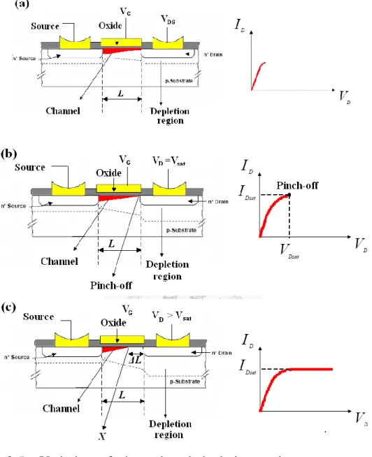
In the first instance, consider the case the voltage between source and drain (VDS) is quite small compared to the voltage between source and gate (VGS). When gate is at zero bias (relative to source), the n+-p-n+ structure can be seen as a reverse cascade of two pn junction diodes and no current flows through the path; NMOS is cut-off, as illustrated in Fig. 2.3 (a). As applying a small positive voltage to gate, the majority carriers (holes) in p-type semiconductor will be repelled and then the depletion region forms in the surface of p-type semiconductor, as illustrated in Fig. 2.3(b). Once
8
gate voltage achieves the threshold voltage (Vth), the inversion layer (channel) exactly appears in the surface of p-type semiconductor and the minority carriers (electrons) start to accumulate in the channel, as illustrated in Fig. 2.3(c). With increasing gate voltage, the number of accumulating electrons increases while the depletion region almost remains constant, as illustrated in Fig. 2.3(d). Fig. 2.4 shows the output characteristics (ID–VDS curves at different gate bias) mentioned above.
The uniform distribution (since VGSVDS) of electrons results in the same effective channel thickness (t) everywhere so the resistance described by RDS=ρL/Wt (ρ for resistivity of p-type semiconductor, L for channel length, W for channel width) is nearly constant and I–V curves looks almost linear or ohmic.
9
Figure 2.3 The depletion region and the channel at different gate bias. (a) VG=0, (b) VG<Vth, (c) VG= Vth, (d) VG>Vth.
Figure 2.4 Output characteristics when VDS is quite small.
What if VDS increases? If VDS increases, VGD becomes smaller than VGS and thus the channel thickness begins to be asymmetric. From Fig.
2.5 (a), it is obviously seen that the channel thickness beside drain is
10
thinner than that beside source. Because of the reduction of the average channel length, the resistance rises and hence the I–V curve starts bending downwards. When VDS achieves VDsat (onset of saturation), the inversion layer beside drain disappears and the channel beside drain is exactly pinched off, as illustrated in Fig. 2.5(b). Beyond VDsat, the pinched-off length of the channel slightly increases (Δ L << L) and depletion region between drain and channel comes into being, as illustrated in Fig. 2.5 (c).
To furthermore explain the saturated behavior beyond VDsat, point X is defined as the place where the inversion layer exactly disappears when VDS
> VDsat, as seen in Fig. 2.5 (c). By definition, VGX is always equal to Vth
and is independent of VDS. Therefore, VXS is also independent of VDS. In addition, the effective channel length and the carrier (electrons) concentration both are less affected by VDS sinceΔ L << L. As a result, ID remains constant when VDS > VDsat.
The typical output characteristics of NMOS are shown in Fig. 2.6 with three marked points (a), (b), and (c) corresponding to Fig 2.5 (a), Fig 2.5 (b) and Fig 2.5 (c), respectively.
Since the channel of NMOS is enhanced to be active by applied gate voltage, such NMOS is an enhancement-mode FET. On the contrary, the channel of depletion-mode FETs is depleted to be inactive by applied gate voltage.
11
Figure 2.5 Variation of channel and depletion region at a constant VG
when (a) VDS < VDsat; (b) VDS = VDsat; (c) VDS > VDsat.
Figure 2.6 Output characteristics.
12
The current-voltage relationship can be expressed as follows [1]. In the non-saturation region, we will obtain
ID = 12μnCOX WL 2 VGS − Vth VDS − VDS2 …………
and, in the saturation region, we will have
ID = 12μnCOX WL VGS − Vth 2………
where μn is the mobility of the electrons in the inversion layer and,
COX = ϵtOX
OX……….
where ϵOX is the permittivity of the oxide and tOX is the thickness of the oxide.
13
2.1.2 Operation of thin film transistors
The operation of TFT and MOSFET is similar in that the current from the source to the drain is modulated by the applied gate electric field.
Current modulation in a TFT or a MOSFET can be explained if the metal-oxide-semiconductor (MOS) part of the TFT is considered as a capacitor [2].
Fig. 2.7 shows the cross-section and energy band diagrams of a MOS capacitor with an n-type semiconductor. Fig. 2.7 (b) shows the equilibrium state, without gate bias applied, for an ideal case in which no charge is present in the insulator or at the insulator/semiconductor interface so that the energy bands are flat.
A positive voltage applied to the gate electrode, as shown in Fig. 2.7 (c), causes the energy bands to bend downwards, hence increasing the electron concentration at the insulator-semiconductor interface. The interface is therefore more conductive than the bulk of the semiconductor.
This mode of operation in which majority carriers, electrons in this case, accumulate at the insulator-semiconductor interface and give rise to the channel current is denoted as the accumulation-mode operation. When a small to moderate negative voltage is applied to the gate electrode, majority carrier electrons are repelled from the insulator-semiconductor interface so that a depletion layer is formed. When a larger negative voltage is applied the gate, as shown in Fig. 2.7 (d), the depletion layer reaches a maximum thickness after which minority carriers, holes in this case, form a conductive channel at the insulator-semiconductor interface. This conductive channel gives rise to what is denoted inversion-mode operation,
14
since the conductivity type is inverted with respect to the semiconductor bulk. MOSFETs usually operate in inversion-mode whereas TFTs operate in accumulation-mode.
Figure 2.7 (a) The cross-section of a MOS capacitor and corresponding energy band diagrams for several biasing conditions: (b) equilibrium, (c) accumulation (VGS > 0 V), and (d) inversion (VGS < 0 V).
Figure 2.8 shows a three terminal n-channel TFT for accumulation-mode operation. A positive voltage is applied to the gate electrode to attract electrons to the insulator-semiconductor interface and
15
forms an accumulation layer. The drain electrode is biased positively with respect to the source to attract electrons from the accumulation channel.
At zero or small positive voltages applied to the drain electrode, the accumulation layer formed, as shown in Fig. 2.8 (a), is uniform from the source end to the drain end of the channel. At a small drain voltage, the TFT operates as resistor where the drain current (ID) increases linearly with increase in the drain voltage (VDS). However, at slightly larger drain voltages, the linear dependence of ID on VDS changes to a quadratic dependence on VDS. This entire regime of TFT operation, where ID
increases with increasing VDS, is called triode or pre-pinch-off. As VDS is further increased, the effective voltage between the gate and drain (VGD) decreases, which decreases the electron concentration at the drain end of the accumulation layer. The drain voltage, at which the accumulation channel is fully depleted of electrons, is called the pinch-off voltage and is denoted as VDsat. When VDS ≥ VDsat, drain voltage has no effect on ID so that the drain current saturates. This is referred to as the post-pinch-off regime, and is shown in Fig. 2.8 (b).
Figure 2.8 An n-channel accumulation-mode TFT operating in (a) pre-pinch-off and (b) post-pinch-off regime.
16
Depending on the gate voltage required to form an accumulation layer, a TFT can be classified as either an enhancement-mode or a depletion-mode device. In enhancement-mode operation of an n-channel TFT, a positive voltage must be applied to the gate electrode to create an accumulation layer at the insulator-semiconductor interface. For depletion-mode operation, the accumulation layer is already present at zero gate voltage. Thus, for an n-channel TFT, a negative gate voltage has to be applied to deplete the accumulation channel and turn the device off.
Therefore, an enhancement-mode device is a “normally-off” device, whereas a depletion-mode device is “normally on”. In an ideal TFT model in which traps are neglected, the TFT would be a depletion-mode device because of the presence of zero-bias carriers (bulk carriers) available for current conduction. However, the presence of empty traps, which must be filled with carriers prior to the formation of the accumulation layer, gives rise to enhancement-mode operation of the TFT [3].
17
2.1.3 Si-based thin film transistors
The structure of conventional a-Si TFTs for commercial TFT-LCDs is illustrated as Fig. 2.9. Typically, there are five to seven steps to make commercial a-Si TFTs and the flow of the fabrication process is also outlined in the inset of Fig. 2.9 [4].
Figure 2.9 Structure of an a-Si TFT and in the inset, the flowchart outlines the processes for making an a-Si TFT array using a bottom-gate TFT structure and an independent storage capacitor.
Obviously, there are significant differences between the structure of a MOSFET and a TFT. Fig. 2.10 shows typical cross-sectional views of a MOSFET and a TFT.
18
Figure 2.10 Cross-sectional view of a (a) MOSFET and (b) TFT.
As evident from Fig. 2.10, the substrate of a TFT is an insulating material, while the substrate of a MOSFET is a semiconductor material (p-type) of opposite polarity as the source and drain diffusions (n-type).
Source and drain contacts to the semiconducting channel material are injecting contacts to the channel in a TFT structure, instead of ohmic contacts to a pn junction as in a MOSFET.
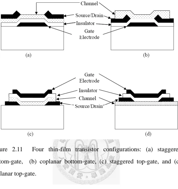
Four TFT device structures are possible, as indicated in Fig. 2.11, and are categorized as staggered or coplanar. In a staggered configuration, as shown in Figs. 2.11 (a) and 2.11 (c), the source/drain contacts are on opposite sides of the channel from the insulator, whereas in a coplanar configuration, as shown in Figs. 2.11 (b) and 2.11 (d), the source/drain contacts and the insulator are on the same side of the channel. Both the staggered and the coplanar configurations can further be classified as bottom-gate and top-gate structures. A bottom-gate TFT, also referred to an inverted TFT, has the gate insulator and gate electrode located beneath the channel, as shown in Figs. 2.11 (a) and 2.11 (b). In a top-gate device,
19
as shown in Figs. 2.11 (c) and 2.11 (d), the channel is covered by a gate insulator and gate electrode.
The coplanar structure is popular in polycrystalline silicon TFTs, whereas staggered structures are commonly used in amorphous silicon TFTs. The inverted, staggered structure is the most popular amorphous silicon TFT structure, because it gives the best transistor characteristics and offers significant process latitude [5].
Top-gate TFTs are usually fabricated with an aluminum gate since gate deposition is one of the last deposition steps in the fabrication process of this type of TFT, after which no high temperature processing is required.
Passivation of the channel material by the gate insulator is an added advantage of a top-gate structure.
20
Figure 2.11 Four thin-film transistor configurations: (a) staggered bottom-gate, (b) coplanar bottom-gate, (c) staggered top-gate, and (d) coplanar top-gate.
As for the performance of a-Si TFTs reported so far, the field-effect mobility reaches from 0.1 to 2 cm2/Vs and the threshold voltage ranges from 2 to 10 V [6-9]. For polysilicon TFTs, the reported mobility can achieve as high as 50 cm2V/s and its threshold voltage is about 1V [10].
However, the fabrication temperature and the opacity of Si-based TFTs limit the possibilities of applications for transparent and/or flexible electronics.
21
2.1.4 Oxide-semiconductor-based thin film transistors
The development of transparent and/or flexible electronics motivates the studies on oxide semiconductor materials such as ZnO [11], SnO2 [12], IGZO (indium gallium zinc oxide) [13], and IZO (indium zinc oxide) [14].
Despite the amorphous structure of these materials, they attract attention mainly due to high electron mobility. Some examples already produce devices with field-effect mobilities reaching above 50 cm2/Vs and on-off ratio of 10-6 to10-7 [11-14].
Table 2.1 summarizes the work regarding wideband gap semiconductors for use as TFTs [12], for this work is directly relevant to the research reported in this thesis.
The use of ZnO channel in the field effect transistor as one of the majority carrier devices has been demonstrated in 1968 with using a bulk single crystal [15]. Notably, it‟s the majority carrier that transports in the channel and no inversion layer is induced by applied gate voltage in the cases of ZnO-based TFTs.
22
Table 2.1 Wide band gap-based TFTs, processing methods employed, and electrical performance characteristics for several different channel materials. The maximum processing temperature, deposition method, mobility, drain current on-to-off ratio, and threshold voltage are included.
Channel Material
Max. Proc.
Temp. (℃)
Dep.
Method
Mobility (cm2/Vs)
On-Off Ratio
Threshold Voltage (V)
Ref.
ZnO Room Temp RFSa 2 106 0 [16]
ZnO 300 PLDb 7 107 0 [17]
ZnO 450 PLD 0.97 105 -1 [18]
ZnO 700 IBSc 2.5 107 10-20 [19]
ZnO 700 SCd 0.2 107 10-20 [20]
(Zn,Mg)O 600 PLD 5.32 103 3 [21]
SnO2 PLD 5 2 -2 [22]
IZO 600 RFS 45-55 106 -20 ~ -10 [14]
ZTO 600 RFS 20-50 107 -5 ~ +5 [23]
IGZO Room Temp PLD 5.6 103 1.6 [13]
a radio frequency sputtering
b pulsed layer deposition
c ion beam sputtering
d spin coating
23
2.1.5 Flexible thin film transistors
There are three main choices for flexible substrates, which include polymeric, thin glass and steel foil. As far as roll-up, lightweight, impact resistance, and cost are concerned, polymeric substrates are the first choice.
A number of issues are discussed for TFTs on polymeric substrates.
Process temperature limitations as a function of polymer type is one of the biggest challenges since polymers undergoing deformation at high temperature conditions invalid the TFTs. The detailed properties of some polymeric substrates are expounded in section 2.3.2.
The popular materials nowadays for channel layer are a-Si, pentacene (organic), and oxide semiconductor such as ZnO. a-Si deposited at limited low temperature achieves poor crystallization and hence quite low mobility, usually less than 2 cm2/Vs. Post-approaches like thermal annealing are needed to improve the electrical performance of a-Si TFTs on plastic. As for organic materials, the low mobility and poor reliability restrain its development while organic TFTs (OTFTs) need lower process temperature.
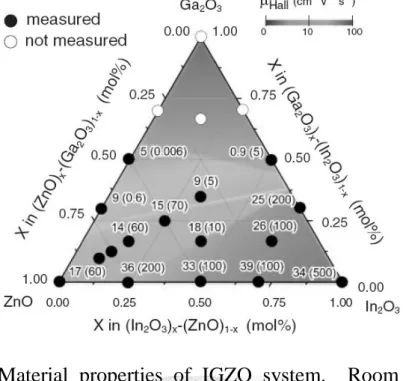
Amorphous and polycrystalline ZnO can be obtained by sputtering at room temperature with high mobility. In addition, the carrier concentration can be engineered by controlling the dopants or the O2 presence. Fig. 2.12 shows the material properties of indium-gallium-zinc oxide (IGZO) system [26].
Table 2.2 summarizes the representative work of flexible TFTs on plastic to date, kinds of popular materials and common substrates included.
24
Figure 2.12 Material properties of IGZO system. Room temperature Hall mobility and carrier concentration as functions of chemical composition. Values outside and inside parentheses show Hall mobility in cm2/Vs and carrier concentration in 1018 cm-3, respectively.
25
Table 2.2 Flexible TFTs on plastic, substrate, processing methods employed, and electrical performance characteristics for several different channel materials. The maximum processing temperature, deposition method, mobility, drain current on-to-off ratio, and threshold voltage are included.
Channel Material
Substratei Max. Proc.
Temp. (℃)
Dep.
Method
Mobility (cm2/Vs)
On-Off Ratio
Threshold Voltage
(V)
Ref.
a-Si:H PEN 120 PECVDe 0.8 106-107 4.5 [24]
a-Si:H 180 PECVD 0.8~1 106 3 [25]
a-IGZO PET Room Temp PLD 10 106 1.3 [26]
ZnO PI Low Temp RFS 50 105 3.2 [27]
ZTO PI 300 RFS 14 106 -8.8 [28]
Pentacene PEN TEg 0.67 104 -0.88 [29]
CNTh Room Temp IPf 47,662 1.08 -2.5 [30]
e plasma-enhanced chemical deposition
f inject printing
g thermal evaporation
h carbon nanotube
i also see section 2.3.2
26
2.2 Property of Materials 2.2.1 Zinc Oxide (ZnO)
ZnO material has drawn much attention recently for its good optical and electrical properties. With such potential advantages as wide bandgap (3.4eV), large exciton binding energy (60meV), high Hall mobility and so on, ZnO is widely studied in various fields such as thin film transistors, transparent conducting electrodes, varistors, ultraviolet emitting diodes, etc.
Besides, ZnO even becomes a popular material for commercial cosmetic products and sunglasses because of its capability of absorption of ultraviolet light.
The property of ZnO is listed in Table 2.3 [31]. Because the bandgap of ZnO is 3.4eV, ZnO is transparent in the visible light. Transparent oxide semiconductor materials make possible replacement of opaque Si as channel layer of TFTs and improvement of aperture ratio of TFT-LCD.
ZnO is a promising candidate among these oxide semiconductors.
Furthermore, polycrystalline ZnO thin film can be achieved at lower growth temperature by methods of sputtering, pulsed laser deposition, chemical vapor deposition, molecular beam epitaxy, and inkjet printing, etc.
Better crystallization means higher mobility and hence higher operating current. In these respects, ZnO is more attractive and feasible than organic- or Si-based TFTs when cheap and/or transparent substrates made of glass or polymer are chosen.
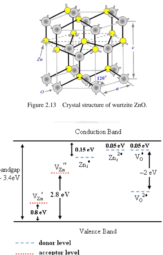
ZnO crystallizes with the wurtzite structure is shown in Fig. 2.13.
27
Table 2.3 Properties of ZnO
Property Value
Crystalline Hexagonal
Lattice parameter at 300K:
a 3.252 Å
c 5.313 Å
c/a 1.602 Å (1.633 for ideal hexagonal structure)
Density 5.606 g/cm3
Stable phase at 300K Wurtzite
Melting point 1975℃
Thermal conductivity 0.6, 1–1.2 Linear expansion coefficient (/℃) a: 6.5× 10⁻⁶
c: 3.0× 10⁻⁶ Static dielectric constant 8.656
Refractive index 2.008, 2.029
Energy gap 3.4eV, direct
Intrinsic carrier concentration < 106 cm-3
Exciton binding energy 60 meV
Electron effective mass 0.24 Electron Hall mobility at 300K for
low n-type conductivity
200 cm2/Vs
Hole effective mass 0.59
Hole Hall mobility at 300K for low p-type conductivity
5–50 cm2/Vs
28
Figure 2.13 Crystal structure of wurtzite ZnO.
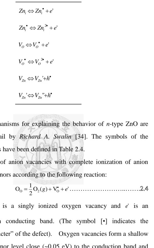
Figure 2.14 Energy levels of native defects in ZnO. The donor defects are
2
Zni , Zni, Zni,VO2,VO,VOand the acceptor defects areVZn'', VZn'.
29
For n-type ZnO, it‟s considered that zinc interstitials (Zni) and oxygen vacancies (VO) act as donors and may account for the n-channel behavior [27]. The model that Zni and VO are indentified as dominant donors in ZnO however is challenged by some novel theory and experiment [32], but others find the amount of O2 when depositing ZnO film does affect the conductivity and carrier concentration of ZnO. The reaction of defects in ZnO is listed in Table 2.4 and the related ionization energy is diagramed in Fig. 2.14 [33].
Table 2.4 (a) For crystal MX, the symbols are defined as:
MM M atom on M site
XX X atom on X site
Mi M atom on interstitial site Xi X atom on interstitial site NM Impurity N on M site VM Vacancy on M site VX Vacancy on X site Vi Vacant interstitial site
e’ Electron in conducting band h‧ Hole in valence band
30
Table 2.4 (b) Reactions of defect ionization in ZnO '
e Zn Zni i
2 ' e Zn Zni i
' e V VO O
2 ' e V VO O
V h VZn Zn'
V h VZn' Zn"
The two mechanisms for explaining the behavior of n-type ZnO are also stated in detail by Richard A. Swalin [34]. The symbols of the following equations have been defined in Table 2.4.
(a) Formation of anion vacancies with complete ionization of anion vacancy donors according to the following reaction:
' V ) ( 2O
OO 1 2 g O e………..…….
where VO is a singly ionized oxygen vacancy and e' is an electron in conducting band. (The symbol [•] indicates the
“hole-character” of the defect). Oxygen vacancies form a shallow electron donor level close (~0.05 eV) to the conduction band and are readily ionized near room temperature, contributing free electrons. This reaction can undergo further ionization with liberation of another electron into the conduction band [27]; that is,
' 2 V ) ( 2O
OO 1 2 g O2 e ………...
31
(b) Formation of ionized cation interstitials according to the following reaction:
' Zn
Zn(g) ie ………..……...
Physically, this corresponds to transferring a neutral zinc atom from the vapor phase to an interstitial position. Interstitial cations tend to act as donors and, in this case, since the donor level (~0.05 eV) lies so close to the conduction band, the interstitials would be completely ionized. There could be a second ionization step according to:
' Zn
Zni 2i e ………..……...
The equilibrium constants for the processes (a) and (b) are:
] ' ][
[ p
Ka O212 VO e ………..………..……...
Zn
i e
Zn p
] ' ][
Kb [
………..……..……...
The quantities pO2and pZn are not independent of each other, since for the reaction for the formation of ZnO,
ZnO(s) (g)
2O
Zn(s)1 2 ………..……...
there is an equilibrium constant
12
p 2
p
K Zn O ………..……...
yielding
12 b [ ][ ']p 2
KK Zni e O ……….………..……...
If pO2decreases, [e'] increases and thereby so is the conductivity .
32
Further evidence concerning the nature of the defect structure comes from self-diffusion studies of Zn in ZnO. From these studies it is found that the diffusion coefficient is very high. The activation energy for the diffusion of Zn in ZnO is 0.55 eV, or 53KJ/g-atom. This value is too low for diffusion by a vacancy mechanism. The only way to explain this fast diffusion is to postulate the existence of interstitial Zn, therefore giving support to alternative (b) above. Since interstitial Zn ions are produced in concentration equal to the electron concentration,
] ' [ ]
[Zni e ………....……...
thus, the conductivity
14
p 2
] '
[
e O
………..……...
33
2.3.2 Indium Tin Oxide (ITO)
So far, the most widely used materials for transparent conducting oxides (TCO) are zinc oxide(ZnO), tin oxide(SnO2), and indium oxide (INO). Compared to ZnO, SnO2, and INO, tin-doped indium oxide (ITO) has lower electrical resistivity (about 10-4Ω cm) and higher optical transparency (above 85% at 550 nm) . As a result, ITO is more and more significant in the field of display devices, photovoltaic cells, and opto-electronic devices.
As an n-type degenerate semiconductor with wide bandgap (3.5 eV ~ 4.3 eV) and high work-function (4.5 eV ~ 5.3 eV), the mechanisms of conductive ITO can be attributed to tin dopants and oxygen vacancies.
The two reactions are described as follows [35]:
' 2 V ) ( 2O
OO1 2 g O2 e………..……...
and
………...
where SnIn denotes the Sn+4 which replaces In+3 site in In2O3 crystal. The rest symbols in these expressions are same as what have been defined in section 2.2.1.
One oxygen vacancy donates two electrons as donors. In addition, since the atom size and mass of tin dopant close to what of indium, it‟s possible for Sn+4 to replace In+3 and then a free electron is formed as a donor. The cubic bixbyite structure of In2O3 crystal (of ITO crystal as well) is illustrated in Fig. 2.15.
34
The need for ITO thin film had led to the development of various deposition techniques. Both vacuum techniques, e.g. evaporation and sputtering, and non-vacuum techniques, e.g. sol-gel and ink-jet printing.
Among numerous methods, magnetron sputtering can deposit films over large areas at higher deposition rate than conventional evaporation and it needs lower fabrication temperature than evaporation. Magnetron sputtering is rationally considered to be one of the best methods for preparing ITO films. High quality ITO films grown by magnetron sputtering have already been reported since 1990‟s [36].
The properties of sputtered ITO are proven to be quite sensitive to sputtering environment, such as substrate temperature [37], target-to-substrate distance [38], pressure of oxygen and/or hydrogen [39], RF power [40], and post-deposition annealing treatment [41].
Figure 2.15 A simplified section of the unit cell of In2O3 (ITO, as well).
The distance between the oxygen atoms varies between 2.8 and 2.9 Å
35
2.2.3 Insulating materials
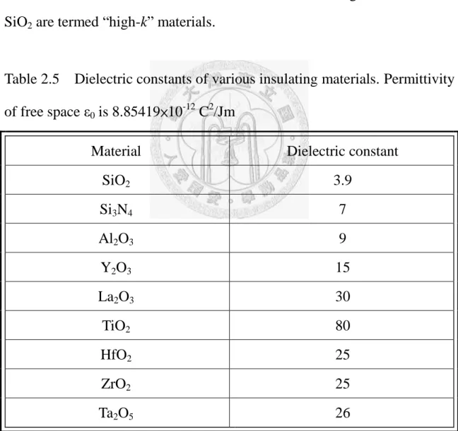
The performance of a TFT is also related with the insulating layer, which can be explained from equation , and . From equation , higher dielectric constant leads to larger capacitance and hence the TFTs can operate in ON and OFF states distinguishably; that is, high current for ON state and low current for OFF state. The dielectric constants of the most commonly used insulating materials are listed in Table 2.5. Those materials with dielectric constants higher than that of SiO2 are termed “high-k” materials.
Table 2.5 Dielectric constants of various insulating materials. Permittivity of free space ε0 is 8.85419×10⁻¹² C2/Jm
Material Dielectric constant
SiO2 3.9
Si3N4 7
Al2O3 9
Y2O3 15
La2O3 30
TiO2 80
HfO2 25
ZrO2 25
Ta2O5 26
36
2.3 Property of Substrates 2.3.1 Glass substrate
The glass substrates for fabrication of TFTs have to satisfy the following demands.
(1) To be alkali-free to prevent alkali ions from diffusing into TFT arrays.
(2) High resistance to chemical solutions such as etchant, developer and cleanser.
(3) Low coefficient of thermal expansion (CTE).
(4) Good Flatness and Surface Quality
Table 2.6 [42] summarizes the characteristics of some glass substrates produced by the main producer in the global world.
Among these glass substrate, Corning 1737 and Corning 7359 are very popular for fabrication of TFTs in lab stage. Table 2.7 provides the property of Corning 1737 [43].
37
Table 2.6 Property of glass substrates produced by famous producer in the global world.
Producer Products Density (g/cm3)
Strain Point (℃)
CTE (Multiply by 10-7cm/cm/℃)
Corning
Eagle 2000 2.370 668 32.5
1737 2.545 666 37.8
7059 2.752 593 46.6
Asahi
AN-100 2.506 670 35.5
AN-635 2.77 635 48
NEG
OA-2 -- -- --
NA-10 2.511 651 36.6
NHT
NA-45 -- -- --
NA-35 2.500 650 36.7
POI POI <2.500 645 32~37
38
Table 2.7 Property of Corning 1737.
Glass Code: Corning 1737
Type Alkali Free Borosilicate
Color Clear
Principal Use Optics & electrical substrates Thermal Expansion
Multiply by 10-7cm/cm/℃
0 - 300℃. 37.6
Viscosity Data
Strain point ℃. 666
Annealing point ℃. 721
Softening point ℃. 975
Density g/cm3 2. 54
Log10 of Volume
Resistivity ohm/cm. 250℃ 13.5
Dielectric Properties (1 KHz 20℃)
Dielectric constant 5.7
Loss factor % .10
Refractive index @ 589 nm 1. 518
Transmittance (t=0.7mm)
~70% (320 nm)
~90% (360 nm)
>90% (380-2600 nm)
39
2.3.2 Polymer substrates [44]
The plastic films that have been given serious consideration as flexible substrate for flexible electronics are show in Fig. 2.16, their abbreviations, glass transition temperature and crystallization included. The glass transition temperature limits the thermal budget of fabrication of electronic devices.
Figure 2.16 Comparison of a range of plastics by glass transition.
The clarity of the film is important for transparent electronics. A total light transmission (TLT) of >85% over 400–800 nm is typical of what is required for this application. All the base films described above meet this criterion, except for PI which is yellow; see table 2.8.
A wide range of solvents and chemicals can be used when fabricating
0 100 200 300 400 500 600
PET PEN PC PES PCO PAR PI
Tg (glass transistion temperature)
Tm (melting temperature)
Temperature (°C)
PET: polyethylene terephthalate PEN: polyethylene naphthalate PC: polycarbonate
PES: polyethersulphone PCO: polycyclic olefin PAR: polyarylates PI: polyimide Biaxially oriented
semicrystalline Amorphous
40
electronic devices on polymer substrates. Amorphous polymers in general have poor solvent resistance compared to semicrystalline polymers;
see table 2.9. This deficiency is overcome by the application of a hardcoat layer (e.g. SiO2, SiNx etc.) double-side coated to the polymer films, which significantly improves the solvent and chemical resistance.
Table 2.8 Basic properties of plastic films used for base substrates. (Note:
The information in this table is taken from different datasheets and should only be taken as illustrative.)
PET PEN PC PES PAR PCO PI
CTE
(-55 to 85 °C) ppm/°C 15 13 60-70 54 53 74 17 Transmission
at 400–700nm (%)
>85 >85 >90 90 90 91.6 yellow Water absorption
(%)
0.14 0.14 0.2-0.4 1.4 0.4 0.03 1.8 Young‟s modulus
(GPa)
5.3 6.1 1.7 2.2 2.9 1.9 2.5 Tensile strength
(MPa)
225 275 NA 83 100 50 231
41
Table 2.9 Solvent resistance of polymer substrates.
Unit PEN PET PC PES
Ketone Acetone Good Good Fair No good MEK Good Good Fair - Alcohol Methanol Good Good Good - Ethanol Good Good Good Good Isopropanol Good Good Good - Butanol Good Good Good - Ester Ethyl acetate Good Good Fair Good Hydrocarbon Formalin Good Good No good -
Tetrachroloethane Good Good - Good Acid 10% HCl Good Good - Good 10% HNO3 Good Good - Good 10% H2SO4 Good Good - Good Acetic acid Good Good - - Alkali 10% NaOH Good Fair - Good
Polymers absorb water and oxygen and the amount of water and oxygen they absorb can have a very detrimental effect on both substrate and electronic devices. In principle, a perfect layer of silica only a few nanometers thick should reduce the diffusion of water and oxygen to acceptable levels (just as the 2–3 nm native oxide layer on silicon wafers protects the wafer surface from further oxidation) although in practice thin film coatings can have defects that provide easy paths for water and oxygen molecules to penetrate. This particularly retards the progress of organic electronic devices in that they require water vapor transmission rate of
<10-6 g/m2 per day and oxygen transmission rates of <10-5 mL/m2 per day and no base polymer at present meets these extremely demanding
42
requirements.
The surface smoothness and cleanliness of the flexible substrates are essential to ensure the integrity of subsequent layers such as barrier and conductive coatings. With PET and PEN films, improvements in surface quality can be achieved through control of recipe and film process. This is demonstrated in Fig. 2.17 [45], which highlights the substantial reduction of surface defect peaks with two different grades of PEN film.
The surface defects which remain in the Teonex Q65, in Fig. 2.17 (b), however, are still detrimental to the performance of thin overlying layers.
To remove them entirely requires the application of a coating layer, typically comprised of a scratch-resistant material. This acts to smooth over all the underlying surface defeats and additionally help to prevent surface scratches on handling.
43
Figure 2.17 Surface roughness of (a) Teonex Q83 and (b) Teonex Q65, films produced by DuPont.
44
2.4 Plasma reaction and sputtering [46]
Plasma is typically a partially ionized gas and is considered to be a distinct state of matter, in contrast to gases because of its unique properties.
The reactions to form plasma in a vacuum system include dissociation, excitation, ionization and glow discharge. For gas X2, the reactions can be expressed as follows:
e−+ X2 → 2X + e− (dissociation)….…..….………
e−+ X → X∗ + e− (excitation) ….…….…………
e−+ X2 → X2∗ + e− (excitation) ….…….…..……
e− + X2 → X2++ 2e− (ionization) …….…...………
e−+ X2 → X2+ + 2e− (glow discharge) ……..……
in which electrons emitted by two parallel electrode plates under DC or AC bias collide with the gas X2 to form plasma.
Plasma generation requires electrons with high kinetic energy K:
K = F ∙ d = q ∙ Ε ∙ λ = q ∙ V
de ∙ λ ….…….…………
where E is electric field, λ is mean free path, V is electrode voltage and de is electrode distance. Thus, plasma is generated in high voltage bias to increase V and in low pressure to increaseλ . Take argon (Ar) for example; the process of plasma generation can be conceptually diagramed as in Fig. 2.18.