行政院國家科學委員會補助專題研究計畫□成果報告 ■ 期中進度報告
過渡性金屬氧化物及硫屬化合物之奈米結構與單晶製備及其特 性研究(2/3)
Growth and Characterization of Nanostructural and Bulk Single Crystals of Transition Metal Dioxide and Dichalcogenides
Compounds
計 畫 類 別 : ■ 個 別 型 計 畫 □ 整 合 型 計 畫 計 畫 編 號 : NSC 97 - 2112 - M - 011 - 0011 - MY3 執行期間: 97 年 8 月 1 日 至 100 年 10 月 31 日
計 畫 主 持 人 : 黃 鶯 聲
計畫參與人員:陳宜民、黃鎮台、林珊杉、蘇宥榛、洪筱芸、劉冠甫 魏宇宣、楊子弦
成果報告類型(依經費核定清單規定繳交):■精簡報告 □完整報告
本 成 果 報 告 包 括 以 下 應 繳 交 之 附 件 :
□ 赴 國 外 出 差 或 研 習 心 得 報 告 一 份
□ 赴 大 陸 地 區 出 差 或 研 習 心 得 報 告 一 份
□ 出 席 國 際 學 術 會 議 心 得 報 告 及 發 表 之 論 文 各 一 份
□ 國際合作研究計畫國外研究報告書一份
處理方式:除產學合作研究計畫、提升產業技術及人才培育研究計畫、列管計畫 及下列情形者外,得立即公開查詢
□涉及專利或其他智慧財產權,□一年□二年後可公開查詢
執行單位:國立台灣科技大學電子工程所
中 華 民 國 99 年 6 月 8 日
一、中文摘要
本期計畫主要使用射頻反應式濺鍍法(RF-reaction sputtering)與有機金屬化學汽相沈積 法(MOCVD)成長過渡性金屬氧化物二氧化鈦(TiO2)、二氧化釕(IrO2)及二氧化銥(RuO2)奈
米結構晶體,並利用X 光繞射(XRD)、、場發射式掃瞄式電子顯微鏡(FESEM)、場發射式
穿透式電子顯微鏡(FETEM)、拉曼散射儀(Raman spectroscopy)、X 射線光電子光譜(XPS)
來檢測所成長之奈米晶體特性。利用XRD 與 FESEM 來探討在不同基板上而產生的奈米晶體成
長方向性與表面形貌, TEM 則用來探討奈米晶體更細微的形貌與結晶結構特性,XPS 分析奈 米晶體之化學鏈結特性。此外,利用拉曼散射光譜(Raman)來檢測奈米結構,並利用 modified spatial correlation (MSC) model 來解析出因為應力與尺寸效應所個別造成拉曼光譜訊號紅移的現 象。另一方面,也利用Chemical vapor transport (CVT)方法成長層狀單晶,利用極化的光導 (photoconductivity)及吸收(absorption)來量測 MoSe2, ReS2等層狀單晶的特性,此外也利用溫度 變化(12K-300K)的實驗來量測此樣品之特性。
關鍵詞:二氧化銥 、二氧化釕、奈米晶體、場發射式電子顯微鏡、 拉曼散射光譜、層狀半導 體、二硒化鉬。
二、英文摘要
We review results of synthesis of well-aligned TiO2, IrO2 and RuO2 nanocrystals (NCs) via reactive magnetron sputtering and metal-organic chemical vapor deposition. The surface morphology and structural properties of the as–deposited NCs were characterized by X-ray diffraction (XRD), field emission scanning electron microscopy (FESEM), and field emission transmission electron microscopy (FETEM) analyzed the detail morphology and crystal structure. X-ray photoelectron spectroscopy determined the composition, chemical state of the NCs. Beside that, Raman scattering has been used as a technique for the characterization of NCs grown on a number of different oriented substrates under various conditions. The redshifts and asymmetric linewidth broadening of the Raman features of IrO2 and RuO2 NCs with respect to that of their bulk counterparts were analyzed by a modified spatial correlation (MSC) model, which includes a factor of stress-induced shift. The MSC model showed that the effects of stress and nanometric size could be separated in analyzing the observed Raman features. The usefulness of experimental RS together with the MSC model analysis as a structural and residual stress characterization technique for NCs has been demonstrated.
Chemical vapor transport (CVT) process with Br2 as a transporting agent has been utilized for growing large size MoSe2 single crystals by adding Re (rhenium) dopant (nominal concentration of 1%) during the growth process. The anisotropy of the conductivity and indirect band gap parallel and perpendicular to the crystal c-axis due to the interlayer van der Waals interaction and red shift of the indirect and direct band gaps due to doping have been measured. It is found that the conductivity anisotropy decreases drastically as a result of doping and the crystal anisotropy has a more pronounced influence on the indirect gap in comparing to the direct gap of the layered crystals. The absorption- edge anisotropy of 2H-MoSe2 was studied by photoconductivity (PC) measurements as a function of temperature in the range of 12–300 K. A significant shift towards lower energies has been observed in the PC spectra on the edge plane with respect to those corresponding to the van der Waals (VdW) plane. The parameters also describe by the temperature dependence of the absorption edges.
Keywords : IrO
2 、 RuO2 、nanocrystals、field emission scanning electron microscopy、 Raman Scattering、layer crystals、MoSe2。三、計畫緣由與目的
近年來,二氧化鈦(TiO2) 也有廣大研究團對投入研究,二氧化鈦具金紅石結構 (Rutile
structure; 簡稱 R-TiO2)與銳鈦礦結構(Anatase structure; 簡稱 A-TiO2) 。此兩不同結構具有不同
的物理與化學特性。近幾年來,在光電、化學及綠色能源工業應用頗受歡迎。其中當為 A-
TiO2,因其化學較強特性,常被用來作為光觸媒應用。R-TiO2,因為有高的介電常數與反射 係數,常被用來當作光學元件或是光電轉換應用。近年來奈米結構之二氧化鈦,因其獨特構 造與及光電、電化學特性使其成為熱門研究主題之一。
IrO2、RuO2 是近來廣為受到注目的新興電極材料。因其氧化物具有導電性,且易於蝕
刻,並可改善PZT 的疲勞及 Pb 的擴散現象,故為目前下一代電極材料的研究重點。屬於釕金
屬的氧化物,二氧化釕(RuO2),在電子工業方面的運用,在 1975 年以後漸受重視,因其本身
雖是氧化物,但具有金屬性的導電性且化性穩定,故受到重視,如以 RuO2 與 CdS 組成蕭特
基界面應用於積體光學,與玻璃混合燒結製成厚膜電阻,利用 RuO2薄膜作為 VLSI 中阻擋鋁
擴散之屏障,利用 RuO2 薄膜與 SrTiO3 製作高效率的 DRAM。雖然二氧化銥及二氧化釕薄膜
有如此多的應用價值,但是研究有關其基本特性之文獻並不多也不完整。有些屬於工業相關 應用之資料,也多被列入專利範圍。可知該材料的確具備相當潛力,也值得做深入研究。然 而,高品質且穩定的二氧化釕與二氧化銥奈米薄膜獲得不易,所以薄膜成長以及檢定技術將 成為本計劃之研究主軸。反應式濺鍍法(reactive sputtering)成長二氧化釕與二氧化銥奈米薄膜 已是目前最廣為研究單位採用以及較為成熟的技術;有機金屬化學汽相沉積法(metal organic chemical vapor deposition;簡稱 MOCVD)則是現今在工業製程上用於大量生產以矽與三五族 化合物半導體為基礎之最佳與最廣泛的晶片製作技術。本計劃將試著藉由反應式濺鍍法及有 機金屬化學汽相沉積法,這兩種技術來比較並取得最適當的薄膜成長方式,並探討其應用在 鐵電記憶體之可能性。
過渡金屬硫屬化合物(Dichalcogenides),層狀結構者:如、二硒化鉬(MoSe2)、 二硫化
鎢(WS2)、 二硒化鎢(WS2)等皆具有半導體之特性。近幾年來,在光電化學及能源工業應用方
面,頗受重視。其中二硫化鉬的用途甚廣,因其本身質軟,潤滑性佳,對高溫高壓的穩定性 好,是其他潤滑劑所無法比擬的。而用於碳氫化合物中,則是加氫、去氫的良好催化劑。近 年來更被用為作石油中加氫去硫(Hydrodesulfurization)的主要觸媒。而在照光後產生 d-d 能 帶間的轉換,不須破壞化學鍵,即不產生光腐蝕(Photocorrosion)的現象,可作為光電化學 太陽電池的理想電極。因此若能有效的探討其基本物性,對於實際應用上極有價值。
四、研究方法
利用有機金屬化學汽相沉積(MOCVD)製作 TiO2、RuO2、IrO2系列之導電性氧化物奈米 晶體乃是以有機金屬作為先驅反應物(precursor),藉由反應氣體(reactive gas)或載氣(carrier gas) 將氣態之先驅反應物帶至欲成長之基板處進行化學反應,並在此過程中藉由固態反應物的沈 積而進行磊晶成長。利用適當地控制進氣流量、基板的反應溫度、成長壓力及其他可控制之 參數,即可蒸鍍出平整度高、化學配比適當以及結構性良好之奈米晶體。濺鍍法製備奈米晶 體乃是以金屬鈦板(99.99 %)、金屬銥板(99.99 %)、金屬釕板(99.99 %)作為靶材。在金屬原子 被離子撞出後,先與氧氣反應成二氧化鈦、二氧化銥、二氧化釕,或在基板上氧化成金屬氧
化物。系統含兩個真空室,使用噴射幫浦及機械式迴轉幫浦,最高真空度約為5 ×10⁻⁵ mbar。
配合 1 英吋、2 英吋兩種靶之直徑,控制基板的反應溫度,另使用純度 99.95 %之氧氣及氬
氣,提供離子與反應氣體。化學汽化傳導法(CVT)為利用過渡性金屬化合物粉末作為長晶
的起始材料,在 1000 ℃以上的溫度下分解後由添加的化性活潑的傳導劑帶到稍微低溫的區域
再結合形成晶體。
X 光繞射分析中使用的是 Japan Rigaku D/Max-RC ,40kV 電壓與 100mA 電
流,散射角度為 20-100°,用以分析在不同基板上而產生的奈米晶體成長方向性。場發射
式掃瞄式電子顯微鏡(FESEM)使用的是 Japan JEOL JSM6500F,電壓為 15kV,用以分析探討 成長方向性與表面形貌。場發射式穿透式電子顯微鏡(FETEM)使用的是於 200kV 的加速電壓
下的Phillips G2 F20 FETEM ,用以提供奈米晶體更細微的形貌與結晶結構特性。在拉曼散射
光 譜 分 析 中 , 使 用 的 是 Renishaw inVia micro-Raman 來 檢 測 奈 米 結 構 , 其 中 包 含 1800grooves/mm 的光柵,50x 的光學透鏡,1.5mW 的 Ar+雷射,譜線將利用 modified spatial
correlation (MSC) model 來解析出因為應力與尺寸效應所個別造成拉曼光譜訊號紅移的現象。
X 光光電子能譜儀為利用 X 光將電子擊出分析此電子能量而得到原宿種類與化學態的資訊,
實驗中使用的是英國VG ESCA Scientific Theta Probe,光源為 Al 靶之 Kα(1486.6eV),配有氬
離子鎗。光吸收與光導可以用來判定樣品的能隙與缺陷,利用Varshni 及 Bose-Einstein 方程式
來得到其溫度變化之相關係數並加以討論。調制光譜量測技術係將待測樣品的外在物理量
(如溫度、壓力、電場或磁場)做微小的週期性改變,或是不改變待測樣品之條件,僅將量 測系統(如入射光波長)做微小的週期性變化,因而得到微分形式的譜線。此具微分形式的 特性,可抑除背景信號及雜訊,使許多難以分辨的微細結構得以清晰分辨,能靈敏地檢測材 料特性,如量子井束縛能階間的躍遷能量,合金成份、材料均勻度、內建電場強度、界面品 質、深階缺陷及其活化能(activation energy)等均可分析求得
六、研究計畫相關成果:
1. Yeh, C. N., Y. M. Chen, C. A. Chen Y. S. Huang, D. S. Tsai, and K. K. Tiong, “Growth and characterization of well-aligned densely-packed rutile TiO2 nanocrystals on sapphire (100) and (012) substrates via reactive magnetron sputtering”, Thin Solid Films, Vol.518, pp.4121~4125 (2010).
Well-aligned densely-packed rutile phase TiO2 nanocrystals (NCs) have been grown on sapphire (100) and (012) substrates by reactive magnetron sputtering using Ti metal target. The surface morphology, structural and spectroscopic properties of the as- deposited NCs were characterized using field-emission scanning electron microscopy (FESEM), X-ray diffraction (XRD), X-ray photoelectron spectroscopy (XPS) and micro-Raman spectroscopy. FESEM micrographs reveal the growth of vertically aligned NCs on sapphire (100), whereas the NCs on sapphire (012) were grown with a tilt angle of 33° from the normal to substrate.
The XRD results reveal TiO2 NCs with either (002) orientation on sapphire (100) substrate or (101) orientation on sapphire (012) substrate. A strong substrate effect on the alignment of the TiO2 NCs growth has been demonstrated and the probable mechanism for the formation of these NCs has been discussed. XPS analyses show the oxygen vs. titanium ratio of 2.0 ± 0.1 for the as-grown TiO2 NCs. Raman spectra of NCs exhibit a slight redshift in the peak position and a small broadening in linewidth with respect to that of the bulk counterpart. The results indicate the formation of good quality of nanocrystalline rutile phase TiO2.
2. Chung, W. H., C. C. Wang, D. S. Tsai, J. C. Jiang, Y. C. Cheng, L. J. Fan, Y. W. Yang, and Y. S.
Huang, “Deoxygenation of IrO2(110) surface: core-Level spectroscopy and density functional
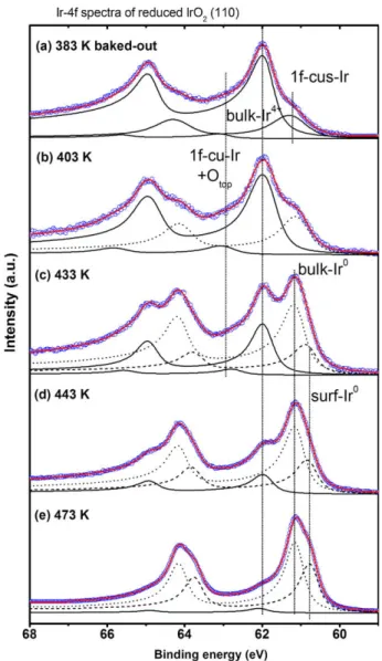
theory calculation”, Surf. Sci., Vol.604, pp.118~124 (2010).Deoxygenation of the IrO2(1 1 0) surface is investigated at 403–493 K, using the core-level spectroscopy and density functional theory (DFT) calculation. The Ir-4f7/2 signals of 1f-cus-Ir with and without on-top oxygen (Otop) emerge as surface features of the baked-out surface, whose positive and negative shifts in binding energy are in line with the DFT computation results.
Progressively increasing the reduction temperature, the 1f-cus-Ir feature quickly disappears and the signal of 2f-cus-Ir emerges at 403 K. Meanwhile the feature of 1f-cus-Ir + Otop diminishes but persists when the Ir metal signal is evident. The intriguing coexistence of 1f-cus-Ir + Otop and Ir metal at 433–443 K is elucidated in the theoretical pathway study. DFT calculation reveals that O2 desorption via pairing two neighboring Otop atoms is the rate-determining step of surface deoxygenation. Under the UHV conditions, Otop is replenished via migration of the surface oxygen species, including the threefold coordinated oxygen (O3f) of a reduced surface. Hence the Otop atom is an active and long-lived surface species, which does not vanish until O3f is consumed and surface Ir begins to cluster. Under the realistic pressure conditions, Otop can also be refreshed via the dissociative adsorption of gas-phase oxygen. In either pathway, Otop is a critical intermediary of IrO2(1 1 0) oxidation catalysis.
3.
Chen, Y. M., C. A. Chen, Y. S. Huang, K. Y. Lee, and K. K. Tiong, “Characterization and enhanced field emission properties of IrO
2-coated carbon nanotube bundle arrays”, Nanotechnology, Vol.21, pp.035702-1~035702-7 (2010).
Low operating electric field and stable emission current have been achieved in IrO2 nanocrystal coated carbon nanotube bundle arrays (CNTBAs). Patterned vertically aligned CNTBAs were synthesized using thermal chemical vapor deposition followed by the deposition of IrO2 nanocrystals by reactive radio frequency magnetron sputtering using an Ir target. The structural and spectroscopic properties were characterized by field emission scanning and transmission electron microscopy, and Raman spectroscopy. The current density versus electric field measurements yielded a low turn-on field of 0.7 V/μm at a current density of 0.1 μA/cm2, a low threshold field of 2.3 V/μm at a current density of 1 mA/cm2, and a high field enhancement factor of 1 x 10⁴ for the IrO2-coated CNTBAs. Long-term stability was also demonstrated. The enhancement of field emission characteristics are attributed to the combined effects of the geometrical structure of the IrO2-coated CNTBAs, and the natural conducting and enhanced resistance to oxidation properties of IrO2.
4. Dumcenco, D. O., Y. M. Chen, Y. S. Huang, and C. H. Ho, “Optical properties of rhenium diselenide single crystals doped with transition metals”, Moldavian Journal of the Physical
Sciences, Vol.8, pp.271~278 (2009).
In this paper, we focus on optical properties of rhenium diselenide (ReSe2) single crystals doped with Au, W, and Nb. The doping effect of the material was characterized by polarization- dependent piezoreflectance (PzR) and photoreflectance (PR) measurements in the temperature range of 15–300 K. The low temperature PzR and PR spectra reveal the observation of E1ex feature at E||b polarization as well as two features E2ex and E3ex at E⊥b polarization. In comparison with the undoped ReSe2, the excitonic transition energies remain practically unchanged, while the broadening parameter of the excitonic transition features slightly increases due to impurity scattering. The angular dependence of the excitonic features amplitudes agree well with the Malus law.
5. Lin, Y. S., K. Y. Lee, K. Y. Chen, and Y. S. Huang, “Superior capacitive characteristics of RuO2
nanorods grown on carbon nanotubes” Appl. Surf. Sci., Vol.256, pp.1042~1045 (2009).
Carbon nanotubes (CNTs) were used as the electric double layer capacitor (EDLC) material and were synthesized by using thermal chemical vapor deposition (TCVD). To enhance the EDLC capacity, the ruthenium dioxide (RuO2) nanorods were grown on CNTs by using metal organic chemical vapor deposition (MOCVD). The synthesized CNTs were the principal part and template, and the RuO2 nanorods were grown outwardly from CNTs. The increase of effective specific area between electrode and electrolyte played an important role in enhancing the capacitance. Different concentrations of KOH were used as electrolyte to measure the capacitance to find the variation of capacitance. Moreover, the RuO2/CNT composites demonstrated a stable cycle life. The results showed that the RuO2/CNT composites were a promising supercapacitor device material.
6. Chen, Y. M., C. A. Chen, Y. S. Huang, K. Y. Lee, and K. K. Tiong, “Synthesis of IrO2
nanocrystals on carbon nanotube bundle arrays and their field emission characteristics”, J. Alloys Compd., Vol. 487, pp.659~664 (2009).
IrO2 nanocrystals (NCs) were deposited on patterned carbon nanotube (CNT) bundle arrays via metal-organic chemical vapor deposition (MOCVD) using (C6H7)(C8H12)Ir as a source reagent. The structural and spectroscopic properties of the IrO2/CNTs composite were characterized by field-emission scanning electron microscopy, Raman spectroscopy and transmission electron microscopy. The combined effects of the geometrical structure of IrO2/CNTs, and the natural conducting and enhanced resistance to oxidation properties of IrO2 lead to a low turn-on field of 0.9 V/μm at a current density of 0.1 μA/cm2, a low threshold field of 2.7 V/μm at a current density of 1 mA/cm2, a high field enhancement factor of 7.4 x 10³, and long-term stability for the IrO2/CNTs composite. The results indicate that the IrO2/CNTs composite can be a potential candidate for field emission devices.
7.
Chen, C. A.,Y. M. Chen, Y. S. Huang, D. S. Tsai, K. K. Tiong, and P. C. Liao, “Synthesis and characterization of well-aligned anatase TiO
2nanocrystals on fused silica via metal organic vapor deposition”, CrystEngComm, Vol.11, pp.2313~2318 (2009).
Well-aligned anatase (A)–TiO2 nanocrystals (NCs) were grown by cold-wall metalorganic chemical vapor deposition (MOCVD) on fused silica using titanium-tetraisopropoxide (Ti(OC3H7)4) as the source reagent. Field emission scanning electron microscopy (FESEM) micrographs showed the growth of vertically aligned NCs. X-ray diffractometry (XRD) pattern revealed the aligned A–
TiO2 with a preferential orientation of (220). Raman spectrum confirmed the deposition of pure anatase phase TiO2 on fused silica. Luminescence of self-trapped excitons and oxygen vacancies were observed in anatase NCs. The indirect band gap of A–
TiO2 was determined to be 3.14 ± 0.01 eV by analyzing the surface photovoltage spectrum. Energy-dispersive X-ray spectroscopy (EDS) and X ray photoelectron spectroscopy (XPS) analyses showed oxygen vs. titanium ratio of 2.0 ± 0.1 for the as-deposited TiO2 NCs. Further structural characterization of the well-aligned A–TiO2 NCs was studied using transmission electron microscopy (TEM) technique. The formation of building units bonded along {112} facets with preferred (220) orientation of the well-aligned A–TiO2 NCs on fused silica were presented and the probable growth mechanisms were discussed.
六、計畫成果自評
本期計畫進行間共發表 7 篇與計劃相關論文(詳見附錄),成果豐碩。研究成果皆發表於
知名的SCI 期刊中,研究成果可供實際運用參考,具學術應用價值。
七、參考文獻
[1] G. R. Patzke, F. Krumeich, and R. Nesper, Angewandte Chemie International Edition, 41 (2002) 2446.
[2] J. Hu, T. W. Odom, and C. M. Lieber, Accounts of Chemical Research, 32 (1999) 435.
[3]
Y. Q. Zhu, W. B. Hu, W. K. Hsu, M. Terrones, N. Grobert, J. P. Hare, H. W. Kroto, D. R. M.
Walton, and H. Terrones, Journal of Materials Chemistry, 9 (1999) 3173.
[4] S. K. Pradhan, P. J. Reucroft, F. Yang, and A. Dozier, Journal of Crystal Growth, 256 (2003) 83.
[5] Y. Liu, J. Dong, and M. Liu, Advanced Materials, 16 (2004) 353.
[6] Z. G. Bai, D. P. Yu, Z. H. Zhang, Y. Ding, Y. P. Wang, X. Z. Gai, Q. L. Hang, G. C. Xiong, and S. Q. Feng, Chemical Physics Letters, 303 (1999) 311.
[7] Y. C. Choi, W. S. Kim, Y. S. Park, S. M. Lee, D. J. Bae, Y. H. Lee, G. S. Park, W. B. Choi, N. S.
Lee, and J. M. Kim, Advanced Materials, 12 (2000) 746.
[8] H. J. Muhr, F. Krumeich, U. P. Schonholzer, F. Bieri, M. Niederberger, L. J. Gauckler, and R.
Nesper, Advanced Materials, 12, (2000) 231.
[9] R. S. Chen, H. M. Chang, Y. S. Huang, D. S. Tsai, S. Chattopadhyay, and K. H. Chen, Journal of Crystal Growth, 271, (2004) 105.
[10] L. F. Mattheiss, Physical Review B, 13, (1976) 2433.
[11] C. U. Pinnow, I. Kasko, N. Nagel, S. Poppa, T. Mikolajick, C. Dehm, W. Hosler, F. Bleyl, F.
Jahnel, M. Seibt, U. Geyer, and K. Samwer, Journal of Applied Physics, 91 (2002) 9591.
[12] J. A. Wilson, A. D. Yoffe, Adv. Phys. 18 (1969) 193.
[13] J. M. Martin, C. Donnet, J. L. Mogne, Phys. Rev. B 48 (1993) 10583.
[14] K. K. Kam, B. A. Parkinson, J. Phys. Chem. 86 (1982) 463.
[15] P. Grange, B. Delmon, J. Less Common Met. 36 (1974) 353.
[16] W. Kautek, J. Phys. C: Solid State Phys. 30 (1982) L519.
[17] H. B. Lian, K. Y. Lee, K. Y. Chen, and Y. S. Huang, Diamond Relat. Mater. 18 (2009) 541
[18] Y. Liu, W. Zhao, and X. Zhang, Electrochim. Acta 53 (2008) 3296
附錄:
Growth and characterization of well-aligned densely-packed rutile TiO
2nanocrystals on sapphire (100) and (012) substrates by reactive magnetron sputtering
C.N. Yeha, Y.M. Chena, C.A. Chena, Y.S. Huanga,
⁎
, D.S. Tsaib, K.K. TiongcaDepartment of Electronic Engineering, National Taiwan University of Science and Technology, Taipei 106, Taiwan
bDepartment of Chemical Engineering, National Taiwan University of Science and Technology, Taipei 106, Taiwan
cDepartment of Electrical Engineering, National Taiwan Ocean University, Keelung 202, Taiwan
a b s t r a c t a r t i c l e i n f o
Article history:
Received 20 March 2009
Received in revised form 5 September 2009 Accepted 9 November 2009
Available online 17 November 2009
Keywords:
Titanium dioxide Oxides
Reactive magnetron sputtering X-ray photoelectron spectroscopy Raman scattering
Well-aligned densely-packed rutile phase TiO2nanocrystals (NCs) have been grown on sapphire (100) and (012) substrates by reactive magnetron sputtering using Ti metal target. The surface morphology, structural and spectroscopic properties of the as-deposited NCs were characterized usingfield-emission scanning electron microscopy (FESEM), X-ray diffraction (XRD), X-ray photoelectron spectroscopy (XPS) and micro-Raman spectroscopy. FESEM micrographs reveal the growth of vertically aligned NCs on sapphire (100), whereas the NCs on sapphire (012) were grown with a tilt angle of∼33° from the normal to substrate. The XRD results reveal TiO2
NCs with either (002) orientation on sapphire (100) substrate or (101) orientation on sapphire (012) substrate. A strong substrate effect on the alignment of the TiO2NCs growth has been demonstrated and the probable mechanism for the formation of these NCs has been discussed. XPS analyses show the oxygen vs. titanium ratio of 2.0 ± 0.1 for the as-grown TiO2NCs. Raman spectra of NCs exhibit a slight redshift in the peak position and a small broadening in linewidth with respect to that of the bulk counterpart. The results indicate the formation of good quality of nanocrystalline rutile phase TiO2.
© 2009 Elsevier B.V. All rights reserved.
1. Introduction
Nanostructured TiO2has been widely studied as a very promising material for applications in photocatalysis[1–5], gas sensors[6–10], solar energy conversion[11–13]and optical devices[14–16]. As a result of these diverse applications, there is a growing need to develop easy and reliable methods for growing different TiO2phases of micro- and nano-crystallized forms. Various techniques have been used for the growth of nanostructured TiO2: magnetron sputtering[17,18], sol–gel processing[19–21], hydrolysis[22,23], thermal evaporation[24–26]
and metal organic chemical vapor deposition (MOCVD) [27–31]. Recently we have successfully grown well-aligned 1D nanostructured TiO2 on different substrates by MOCVD [31]. However, MOCVD generally requires multiple processing steps to fabricate nanostructures.
Proper control of these processing steps can be difficult. For example, the properties of the precursor might change due to oxidation after a few running of the growth process. To overcome such deficiency, we have developed the technique of reactive radio frequency magnetron sputtering. The technique is a simple method to fabricate large area structures and has several advantages including better control of the growth conditions and a single deposition step to obtain the nanostructures.
In this work, we report the deposition of 1D well-aligned densely- packed rutile (R)-TiO2 NCs by reactive radio frequency magnetron sputtering using a Ti metal target on sapphire (100) and (012) sub- strates. The growth behavior of TiO2is found to be highly correlated with the pressure, radio frequency (rf) power, substrate temperature, and orientations of the substrates. The surface morphology, structural and spectroscopic properties of the as-deposited NCs were examined by using field-emission scanning electron microscopy (FESEM), X-ray diffraction (XRD), X-ray photoelectron spectroscopy (XPS) and micro- Raman spectroscopy. A strong substrate effect on the alignment of the TiO2NRs has been observed, and the probable mechanisms for the formation of NR structures are discussed.
2. Experimental details
2.1. Deposition of R-TiO2nanocrystals
Rutile phase TiO2NCs deposition was carried out using a home-made high vacuum radio frequency magnetron sputtering system. The sputtering gun has a standard circular planar magnetron. The sputtering target was a 2-inch Ti (99.95%) metal. The substrates used in this study were sapphire (100) and (012). The substrates had the dimensions
∼10×10 mm2and one side polished. Each substrate was pretreated through a standard cleansing procedure: consecutive cleansing with acetone and methanol in an ultrasonic bath for 10 min to prevent any contamination on the substrate surface. A manually controlled shutter Thin Solid Films 518 (2010) 4121–4125
⁎ Corresponding author. Tel.: +886 2 27376385; fax: +886 2 27376424.
E-mail address:[email protected](Y.S. Huang).
0040-6090/$– see front matter © 2009 Elsevier B.V. All rights reserved.
doi:10.1016/j.tsf.2009.11.014
Contents lists available atScienceDirect
Thin Solid Films
j o u r n a l h o m e p a g e : w w w. e l s e v i e r. c o m / l o c a t e / t s f
was located in front of the target. The sputtering power supply had a maximum output of 300 W. Two separate gas lines, each equipped with a massflow controller, were used to control the Ar and O2flow rates with an accuracy of 0.1 standard cubic centimeters per minute (sccm) for both gases. The sample holder was approximately 45 mm from the target and can be heated to a maximum temperature of 550 °C. To promote uniform transfer of heat to the substrates, a thin coating of melted In was placed between the substrate and the sample holder. Care was being taken to confine all the In metal only to the back of the substrate.
The sputtering chamber was evacuated with a turbo-molecular pump and had a base pressure of∼3×10⁻³Pa. Reactive sputtering was carried out in a mixture of argon and oxygen. For better oxidation of reactive sputtered Ti atom under the surface of the samples, the oxygen line was extended to the substrate holder. Thus O2was introduced over the substrate into the sputtering chamber with Ar atmosphere.
The sputtering parameters for sapphire (100) and sapphire (012) were O2/Ar = 1/1 and 1/5 (rate of O2flow of 10 and 2 sccm, respectively for the two substrates) corresponding to sputtering pressures of 14 and 8 Pa, respectively. The applied rf power was 230 W and the deposition time was 180 min. The substrate temperature Ts was maintained at 400 °C throughout the entire sputtering process.
2.2. Characterization of R-TiO2nanocrystals
The TiO2NCs morphology was studied with a JEOL-JSM6500Ffield- emission scanning electron microscope with an accelerating voltage of 15 kV. The dimensions and growth rates of various TiO2samples were estimated according to the recorded 90° cross-sectional FESEM images.
Crystal structures and overall out-plane orientation of the samples were analyzed using a Rigaku D/Max-RC X-ray diffractometer (XRD) equipped with Cu Kα radiation source, Ni filter and scintillation counter probe SC-30 as a detector. XRD data was collected in Brag Brentano configuration with a step size 2Θ=0.01°. The chemical binding state of the TiO2samples was investigated from Ti 2p and O 1 s spectra obtained by XPS using the Al Kα1486.68 eV as a radiation source in a Thermo VG Scientific Theta Probe system under the base pressure of 10−7Pa. The Ag 3d5/2 line at 368.26 eV was the calibration reference. XPS peak positions and integrated intensities were obtained through curvefitting, using Thermo VG Scientific: Avantage v3.2 software. The Raman spectra were recorded at room temperature utilizing the back-scattering mode on a Renishaw inVia micro-Raman system with 1800 grooves/mm grating and an optical microscope with a 50× objective. The Ar+laser beam of the 514.5 nm excitation line with a power of∼1.5 mW was focused onto a spot size∼5 μm in diameter. Prior to the measurement, the system was calibrated by means of the 520 cm−1Raman peak of a polycrystalline Si.
3. Results and discussion
3.1. Structure of R-TiO2 nanocrystals on sapphire (100) and (012) substrates
3.1.1. R-TiO2on sapphire (100)
As illustrated inFig. 1(a), the FESEM images show the growth of densely populated and vertically well-aligned columnar structure with lateral size of about 55 nm and an average length of about 680 nm TiO2
NCs on sapphire (100) substrate. The typical XRD pattern of the vertically aligned rutile TiO2NCs grown on sapphire (100) depicted in Fig. 1(b) shows the preferable orientation of the nanostructures along TiO2[001] (2θ ∼62.8°). Here we observe anisotropic growth and as a result, NCs formation is restricted by the in-plane mismatch. Thus, the deposited Ti and O atoms are stacked into a 1D nanostructure along c-direction with TiO2plane formation following the substrate orien- tation. Similar growth behavior of R-TiO2, IrO2and RuO2grown on sapphire (100) by MOCVD were observed by our group earlier[31–33].
The preferable oriented growth of R-TiO2(001) along [001] can be explained by examining the TiO2and sapphire (100) planar structure at the atomic level. The unidirectional growth of the NCs is correlated to the epitaxial relation between the rutile lattice of TiO2 and the underlying single-crystal sapphire (001) substrate. The main assump- tion is that there are oxygen vacancies at the sapphire (100) surfaces.
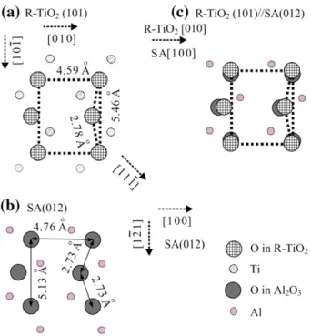
The schematic diagrams illustrated inFig. 2show the atomic arrange- ments on TiO2(001) and sapphire (100) planes. The lattice parameters for TiO2 are a =b = 4.59 Å and c = 2.96 Å [JCPDS No.21-1276], for sapphire they are a =b = 4.76 Å and c = 12.99 Å [JCPDS No. 10-0173].
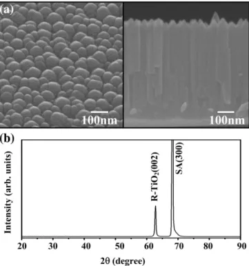
The incoming Ti atoms have sufficient mobility to minimize the lattice Fig. 1. (a) FESEM images (30º perspective- and cross-sectional-view) and (b) XRD pattern of rutile TiO2(001) NCs grown on sapphire (SA) (100) substrate by reactive magnetron sputtering.
Fig. 2. Schematic plots of the lattice relationships between vertically aligned rutile TiO2
NCs and sapphire (SA) (100) substrate: (a) R-TiO2(001); (b) SA(100); (c) R-TiO2(001) on SA(100).
4122 C.N. Yeh et al. / Thin Solid Films 518 (2010) 4121–4125
misfit and align themselves in TiO2(001) arrangement because of the similar oxygen arrangement of underlying substrates and that of TiO2
(001). Thus, the growth relationship can be described as TiO2(001) [100] // sapphire (100)[010]. These alignments produce residual stress due to mismatch values of −3.57% {[(4.59–4.76)Å/4.76 Å]} along sapphire [010], and +5.76% {[(4.59–4.34)Å/4.34 Å]} along sapphire [001] for the NCs grown on sapphire (100). Therefore, we conclude that the vertical growth of TiO2NCs on sapphire (100) substrate, on which the template for TiO2(001) planes formation is facilitated, is dictated by the c-axis directional growth together with the lattice mismatch minimizing mechanism[32].
3.1.2. R-TiO2on sapphire (012)
The micrographs of densely-packed TiO2NCs on sapphire (012) are illustrated inFig. 3(a). The FESEM images reveal the growth of titled columnar structure with lateral size of about 85 nm and an average length of about 860 nm TiO2NCs on sapphire (012) substrate.
These column-like nanostructures exhibit regularly tilted NCs with identical tilt angle (∼33°) from the normal to substrate. The possible explanation of this unique directional growth will be discussed below.
Fig. 3(b) shows typical XRD patterns of the regularly tilted TiO2NCs deposited on sapphire (012). Two peaks can be indexed as (101) and (202) diffraction planes at 2θ around ∼36.0° and ∼76.2°, respectively.
The observation indicates parallel in-plane TiO2(101) orientation. For this particular case, anisotropic growth has been observed resulting in NCs formation restricted by the in-plane mismatch mechanism. Thus, the deposited Ti and O atoms are stacked into 1D nanostructure alongc- direction with TiO2plane formation following the substrate orientation with the growth relation TiO2(101) // sapphire (012).
To determine the directions of planar deposition we have to examine the atomic arrangements of appropriate surfaces.Fig. 4illustrates the schematic plots of the atoms arrangements and lattice relationships between TiO2 (101) and sapphire (012) surfaces. According to the argument of the minimization of the oxide sublattice structural mismatch, the possible NCs-substrates alignment can be described as TiO2(101)[010] // sapphire (012)[100]. The alignments mentioned
above produce directional mismatches of−3.57% {(4.59 Å–4.76 Å)/
4.76 Å} and +6.43% {(5.46 Å–5.13 Å)/5.13 Å} along TiO2[010] and TiO2
[101̅], respectively, on sapphire (012). Concluding this part of the study, we noted that the mechanisms responsible for conversion fromfilm to nanocrystal and the well-aligned directional growth of the nanocrystals are guided by internal and/or external factors. The c-directional growth mechanism is referred as the internal factor and has it origin from the anisotropy of the crystal structure and results in different growth rate along different directions of NCs. The other parameters such as deposition conditions (RF power, substrate temperature, sputtering pressure) and substrate orientations are classified as the external factors. The minimization of the oxide sublattice structural mismatch as dictated by the substrate orientation and the c-directional growth mechanism are the two main driving forces which can determine the alignment and the formation of either tilted or vertical TiO21D NCs.
The external factors of substrate orientation, substrate temperature, and sputtering pressure are responsible for conversion fromfilm to nanocrystals. It is quite apparent that these external factors have an overlapping influence on the internal factor of energetically favorable surface for the incoming atoms (c-directional growth mechanism) and initiate the preferable plane orientation of TiO2 NCs, whereby the incoming atoms will stick onto the lower energy sites.
3.2. XPS investigation
X-ray photoelectron spectroscopy is frequently used as a comple- mentary technique for assigning oxidation states and the stoichiometry of the oxides. TiO2has been reported to be relative easy to handle experimentally[34]. Although it has a bulk band gap of 3.1 eV, no charging problems occur during XPS measurements due to possible oxygen dissociation under ultra-high vacuum and/or surface carbon contamination of the samples.Fig. 5depicts slow scan XPS spectra in the vicinity of (a) C 1 s, (b) Ti 2p and (c) O 1 s regions before (curve I) and after (curve II) Ar ion bombardment. The Gaussian and Lorentzian mixing line shape after the treatment of background by Shirley function has been used in thefitting to determine the accurate peak positions.
As shown inFig. 5(a) a carbon C 1s peak at a binding energy of 284.5 ± 0.1 eV is observed before ion bombardment (curve I). The Fig. 3. (a) FESEM images (30º perspective- and cross-sectional-view) and (b) XRD
pattern of rutile TiO2(101) NCs grown on sapphire (SA) (012) substrate by reactive magnetron sputtering.
Fig. 4. Schematic plots of the lattice relationships between rutile TiO2(101) NCs and sapphire (SA) (012) substrate: (a) R-TiO2(101); (b) SA (012); (c) R-TiO2(101) on SA (012).
C.N. Yeh et al. / Thin Solid Films 518 (2010) 4121–4125 4123
presence of this peak is related to surface pollution which corresponds to the fact that the sample is exposed to air before the XPS measure- ments. The area of the C 1s peak decreases upon ion bombardments (see curve II). This signature persists even after a prolonged ion bombardment of duration much longer than the one known to be necessary for removal of the surface pollution on single crystal titanium dioxide surfaces[35].
It can be seen inFig. 5(b), before Ar ion bombardment the Ti 2p3/2
curve is composed of a single peak at a binding energy of 459.1 ± 0.1 eV,
with a fullwidth at half maximum of 1.3 ± 0.1 eV. The separation between the Ti 2p3/2and Ti 2p1/2is 5.6 ± 0.2 eV. The O 1s binding energy is 530.2 ± 0.1 eV. These results are in good agreement with that of single crystal TiO2(110)[36]. The stoichiometry is determined by the relative areas of the total Ti 2p and O 1s XPS peaks with the correction of the relative sensitivity factors. The oxygen vs. titanium ratio of 2.0 ± 0.1 is obtained. After argon bombardment, the Ti 2p3/2 peak showed a shoulder on the low binding energy side, which was evidenced by the presence of Ti3+[37], indicating that the surface has become non- stoichiometric. The result is a consequence of the removal of oxygen from the surface caused by the preferential sputtering phenomenon [38].
InFig. 5(c), two oxide states attributed to O2−and OH−species are observed from the as-deposited NCs (curve I). However, the OH− shoulder disappeared after Ar ion sputtering (curve II) and the main O 1s feature shifted its binding energy to the reference value of O2−peak [36]. This indicates that the OH−peak is just a surface contamination peak probably due to water adsorption in the air. Similar XPS spectra (peak positions and broadening parameters) were also obtained for TiO2 NCs grown on sapphire (012) substrate. However, the intensity of the O 1 s and Ti 2p core level emissions for TiO2NCs grown on sapphire (012) substrate is about 20% lower than that grown on (100) plane.
This difference in intensity is expected in view of the different surface morphology of the (001) and (101) orientated NCs.
3.3. Raman scattering investigation
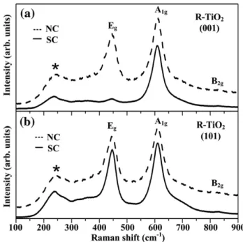
Fig. 6(a) and (b) shows the Raman spectra (dashed curves) of as- deposited R-TiO2NCs samples on sapphire (100) and (012), respec- tively. For comparison purpose, the Raman spectra (solid curves) for R- TiO2(001) and (101) single crystal plates (MTI crystals, Richmond, CA, USA) are also included inFig. 6. Rutile TiO2is tetragonal and belongs to the space group D4h14with two TiO2molecules per unit cell. There are four Raman-active modes with symmetry of A1g, B1g, B2g, and Eg[39]. These four Raman-active modes of rutile TiO2single crystal were detected at 143 cm− 1(B1g), 447 cm−1(Eg), 612 cm− 1(A1g), and 826 cm−1(B2g) by Porto et al.[40]. In addition several second order Raman bands were also observed. As can be seen inFig. 6, the spectra exhibit three distinct broad peaks and a broad weak underlying continuum tailing off at higher
Fig. 5. Slow scan XPS spectra in the vicinity of (a) C 1 s, (b) Ti 2p and (c) O 1 s regions before (curve I) and after (curve II) Ar ion bombardment for R-TiO2(001).
Fig. 6. Raman spectra of (a) R-TiO2(001) NCs on sapphire (100) (dashed curve) and R- TiO2(001) single crystal plate (solid curve), and (b) R-TiO2(101) NCs on sapphire (012) (dashed curve) and R-TiO2(101) single crystal plate (solid curve).
4124 C.N. Yeh et al. / Thin Solid Films 518 (2010) 4121–4125
Raman shifts, and are in good agreement with the features corresponding to rutile TiO2[40]. The major features are the Egand A1g modes located at 445 and 608 cm−1 with full width at half maximum (FWHM) of 38 and 49 cm− 1, respectively, along with the two-phonon bands at∼237 cm−1(marked as *). The Raman spectra exhibits soft B2gmode located at around 823 cm−1and B1gmode is completely absent. The results of Raman scattering measurements confirm the rutile phase of the as-deposited NCs. NCs exhibit a slight redshift in the peak position and a slight broadening in linewidth as compared with the SC (Egat 447 cm− 1, FWHM∼35 cm− 1; A1g at 610 cm− 1, FWHM∼39 cm−1). The results indicated the formation of good quality rutile phase nanocrystalline TiO2. Relative Raman intensities of the Eg, A1g, and B2g phonon modes for the various polarization configurations for R-TiO2are similar to that for IrO2and RuO2and can be found elsewhere[41]. The selection rules maintain that Eg, A1g, and B2gmode are allowed for all polarization configurations for the (101) plane, and the Egmodes is forbidden for all configurations from the scattering of (001) planes. The appearance of Raman signal of the normally forbidden mode might indicate observation of the scattering from the other planes of the NCs as evidenced from the pyramidal shape of the nanostructures' tips.
4. Summary
Well-align densely-packed TiO2NCs have been grown on sapphire (100) and (012) substrates via by reactive radio frequency magnetron sputtering using Ti metal target. We demonstrate that reactive radio frequency magnetron sputtering is a simple method which has several advantages including better control of the growth conditions and a single deposition step to obtain the nanostructures. The results of the structural study reveal that the vertically aligned NCs were deposited on sapphire (100), while the NCs on the sapphire (012) were grown with a tilt angle of∼33° from the normal to substrates. The strong substrates effect on the TiO2NCs alignment can be explained by the effects of minimization of the oxide sublattice structural mismatch overlapped with the c-directional growth mechanism. XPS analyses reveal oxygen vs. titanium ratio of 2.0 ± 0.1 for the as-grown TiO2NCs.
The Raman spectra show the formation of good quality rutile-phase nanocrystalline TiO2.
Acknowledgements
The authors wish to acknowledge the support of the National Science Council of Taiwan under Contract No. NSC 97-2112-M-011- 001-MY3.
References
[1] S.P. Albu, A. Ghicov, J.M. Macak, R. Hahn, P. Schmuki, Nano Lett. 7 (2007) 1286.
[2] X. Zhang, M. Jin, Z. Liu, D.A. Tryk, S. Nishimoto, T. Murakami, A. Fujishima, J. Phys.
Chem. C 111 (2007) 14521.
[3] A.R. Armstrong, G. Armstrong, J. Canales, R. Garcia, P.G. Bruce, Adv. Mater. 17 (2005) 862.
[4] K. Hashimoto, H. Irie, A. Fujishima, Jpn. J. Appl. Phys. Part 1 44 (2005) 8269.
[5] A. Fujishima, T.N. Rao, D.A. Tryk, J. Photochem. Photobiol. C 1 (2000) 1.
[6] L. Francioso, D.S. Presicce, M. Epifani, P. Siciliano, A. Ficarella, Sens. Actuators B 107 (2005) 563.
[7] A. Kolmakov, M. Moskovits, Annu. Rev. Mater. Res. 34 (2004) 151.
[8] O.K. Varghese, C.A. Grimes, J. Nanosci. Nanotechnol. 3 (2003) 277.
[9] C. Garzella, E. Bontempi, L.E. Depero, A. Vomiero, G. Della Mea, G. Sberveglieri, Sens. Actuators B 93 (2003) 495.
[10] C. Garzella, E. Comini, E. Tempesti, C. Frigeri, G. Sberveglieri, Sens. Actuators B 68 (2000) 189.
[11] K. Fujihara, A. Kumar, R. Jose, S. Ramakrishna, S. Uchida, Nanotechnology 18 (2007) 365709.
[12] B. Tan, Y.Y. Wu, J. Phys. Chem. B 110 (2006) 15932.
[13] B. O'Regan, M. Grätzel, Nature 353 (1991) 737.
[14] O.V. Sakhno, L.M. Goldenberg, J. Stumpe, T.N. Smirnova, Nanotechnology 18 (2007) 105704.
[15] R. Rabady, I. Avrutsky, Appl. Opt. 44 (2005) 378.
[16] A. Richel, N.P. Johnson, D.W. McComb, Appl. Phys. Lett. 76 (2000) 1816.
[17] P. Zeman, S. Takabayashi, Thin Solid Films 433 (2003) 57.
[18] G.R. Gu, Z. He, Y.C. Tao, Y.A. Li, J.J. Li, H. Yin, W.Q. Li, Y.N. Zhao, Vacuum 70 (2003) 17.
[19] S. Cerneaux, X. Xiong, G.P. Simon, Y.B. Cheng, L. Spiccia, Nanotechnology 18 (2007) 055708.
[20] D. Liu, M.Z. Yates, Langmuir 23 (2007) 10333.
[21] Z. Miao, D. Xu, J. Ouyang, G. Guo, X. Zhao, Y. Tang, Nano Lett. 2 (2002) 717.
[22] S. Qourzal, A. Assabbane, Y. Ait-Ichou, J. Photochem. Photobiol. A 163 (2004) 317.
[23] W.F. Zhang, M.S. Zhang, Z. Yin, Phys. Status Solidi A 179 (2000) 319.
[24] J.M. Wu, H.C. Shih, W.T. Wu, Chem. Phys. Lett. 413 (2005) 490.
[25] J.M. Wu, W.T. Wu, H.C. Shih, J. Electrochem. Soc. 152 (2005) G613.
[26] J.M. Wu, H.C. Shih, W.T. Wu, J. Vac. Sci. Technol. B 23 (2005) 2122.
[27] P. Evans, M.E. Pemble, D.W. Sheel, Chem. Mater. 18 (2006) 5750.
[28] L.A. Brook, P. Evans, H.A. Foster, M.E. Pemble, A. Steele, D.W. Sheel, H.M. Yates, J. Photo. Chem. A 187 (2007) 53.
[29] M.K. Lee, J.J. Huang, T.S. Wu, Semicond. Sci. Technol. 20 (2005) 519.
[30] J.J. Wu, C.C. Yu, J. Phys. Chem. B 108 (2004) 3377.
[31] C.A. Chen, Y.M. Chen, A. Korotcov, Y.S. Huang, D.S. Tsai, K.K. Tiong, Nanotechnology 19 (2008) 075611.
[32] R.S. Chen, A. Korotcov, Y.S. Huang, D.S. Tsai, Nanotechnology 17 (2006) R67.
[33] C.C. Chen, R.S. Chen, T.Y. Tsai, Y.S. Huang, D.S. Tsai, K.K. Tiong, J. Phys., Condens.
Matter 16 (2004) 8475.
[34] J.T. Mayer, U. Diebold, T.E. Madey, E. Garfunkel, J. Electron Spectrosc. Relat. Phenom.
73 (1995) 1.
[35] S. Bourgeois, P. Le Seigneur, M. Perdereau, Surf. Sci. 328 (1995) 105.
[36] S. Pétigny, B. Domenichini, H. Mostéfa-Sba, E. Lesniewska, A. Steinbrunn, S.
Bourgeois, Appl. Surf. Sci. 142 (1999) 114.
[37] W. Göpel, J.A. Anderson, D. Frankel, M. Jaenig, K. Phillips, J.A. Schäffer, G. Rocker, Surf. Sci. 139 (1984) 333.
[38] G. Betz, G.K. Wehner, Sputtering by Particle Bombardment II, in: R. Behrisch (Ed.), Topics in Applied Physics, vol. 52, Springer-Verlag, Berlin, 1983, p. 11.
[39] R. Loudon, Adv. Phys. 13 (1964) 423.
[40] S.P.S. Porto, P.A. Fleury, T.C. Damen, Phys. Rev. 154 (1967) 522.
[41] A.V. Korotcov, Y.S. Huang, K.K. Tiong, D.S. Tsai, J. Raman Spectrosc. 38 (2007) 737.
C.N. Yeh et al. / Thin Solid Films 518 (2010) 4121–4125 4125
Deoxygenation of IrO
2(1 1 0) surface: Core-level spectroscopy and density functional theory calculation
Wen-Hung Chunga, Chia-Ching Wanga, Dah-Shyang Tsaia,*, Jyh-Chiang Jianga, Yu-Chang Chenga, Liang-Jen Fanb, Yaw-Wen Yangb, Ying-Sheng Huangc
aDepartment of Chemical Engineering, National Taiwan University of Science and Technology, Taipei 10607, Taiwan
bNational Synchrotron Radiation Research Center (NSRRC), Hsinchu Science Park, Hsinchu 30076, Taiwan
cDepartment of Electronic Engineering, National Taiwan University of Science and Technology, Taipei 10607, Taiwan
a r t i c l e i n f o
Article history:
Received 10 September 2009
Accepted for publication 29 October 2009 Available online 31 October 2009
Keywords:
Iridium Catalysis Surface reaction Core-level spectroscopy
Density functional theory calculations
a b s t r a c t
Deoxygenation of the IrO2(1 1 0) surface is investigated at 403–493 K, using the core-level spectroscopy and density functional theory (DFT) calculation. The Ir-4f7/2signals of 1f-cus-Ir with and without on-top oxygen (Otop) emerge as surface features of the baked-out surface, whose positive and negative shifts in binding energy are in line with the DFT computation results. Progressively increasing the reduction tem- perature, the 1f-cus-Ir feature quickly disappears and the signal of 2f-cus-Ir emerges at 403 K. Meanwhile the feature of 1f-cus-Ir + Otopdiminishes but persists when the Ir metal signal is evident. The intriguing coexistence of 1f-cus-Ir + Otopand Ir metal at 433–443 K is elucidated in the theoretical pathway study.
DFT calculation reveals that O2desorption via pairing two neighboring Otopatoms is the rate-determining step of surface deoxygenation. Under the UHV conditions, Otopis replenished via migration of the surface oxygen species, including the threefold coordinated oxygen (O3f) of a reduced surface. Hence the Otop
atom is an active and long-lived surface species, which does not vanish until O3fis consumed and surface Ir begins to cluster. Under the realistic pressure conditions, Otopcan also be refreshed via the dissociative adsorption of gas-phase oxygen. In either pathway, Otopis a critical intermediary of IrO2(1 1 0) oxidation catalysis.
Ó 2009 Published by Elsevier B.V.
1. Introduction
The research interest on deoxygenation of IrO2surface and its spectroscopic signatures stems from curiosity on the reputed cata- lytic properties of Ir and IrO2. The metallic Ir clusters supported by CeO2were reported to exhibit high activity and desirable selectiv- ity in the preferential CO oxidation by O2in excess hydrogen[1].
The strong support effect was understood as CeO2fed the Ir metal with oxygen under an oxygen lean condition. Other support effects have also been described in Ir catalysis toward the CO oxidation and the simultaneous oxidation of soot and NOx[2]. In studying the structural effect on CO oxidation, an oxidized Ir(1 1 0) surface was demonstrated to sustain the rapid reaction rate at steady state [3]. The surface oxide of oxidized Ir was assumed responsible for such an activity toward CO oxidation reaction. One probable struc- ture for this surface oxide is the rutile of IrO2bulk phase, which has been verified on the oxidized Ir(1 1 1) facet[4]. IrO2 is the only solid oxide of iridium with sufficient stability, also known as an
electrocatalyst for oxidation reaction. When incorporated with RuO2in the dimensionally stable anode, IrO2is considered more corrosion resistant but slightly less active than RuO2[5].
Recent studies on the pressure gap of platinum group metals have pointed out that the surface oxide is an integral part of their oxidation catalysis under realistic pressure conditions. Evidences of the Ru[6], Pt[7], Pd[8]surface oxides, which were often ignored under ultrahigh vacuum (UHV) conditions, bridged the gap be- tween the knowledge gathered under UHV and that under the real- istic pressure conditions. The catalytic role of RuO2is a prominent example. A combination of UHV surface techniques and density functional theory (DFT) calculations have achieved an atomic-level understanding on the active sites of RuO2[9]. Being an oxide of platinum group metal, IrO2 shares many similarities with RuO2. Our previous studies on the catalysis of Pt/Ir/IrO2 and Pt/Ru/Ir/
IrO2 in methanol and ethanol electro-oxidation have motivated us to further explore the fine details of IrO2surface and its reduced surface[10]. In this work, we subtract oxygen of the IrO2(1 1 0) surface step by step and study the Ir-4f features of core-level spec- tra (CLS) at various oxidation states. The DFT calculation assists in identifying the CLS features meanwhile sheds light on the path- ways in surface deoxygenation process.
0039-6028/$ - see front matter Ó 2009 Published by Elsevier B.V.
doi:10.1016/j.susc.2009.10.027
*Corresponding author. Address: Department of Chemical Engineering, National Taiwan University of Science and Technology, 43, Keelung Road, Section 4, Taipei 10607, Taiwan. Tel.: +886 2 27376618; fax: +886 2 27376644.
E-mail address:[email protected](D.-S. Tsai).
Contents lists available atScienceDirect
Surface Science
j o u r n a l h o m e p a g e : w w w . e l s e v i e r . c o m / l o c a t e / s u s c
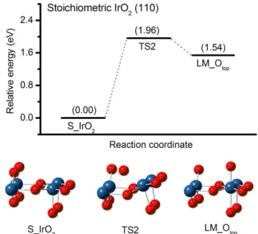
![Fig. 1a presents the atomic model of an oxygen rich (O-rich) sur- sur-face, on which two on-top oxygen (O top ) atoms are adsorbed along the [0 0 1] direction of rutile crystal](https://thumb-ap.123doks.com/thumbv2/9libinfo/9123749.408306/13.892.478.836.753.1080/presents-atomic-oxygen-oxygen-adsorbed-direction-rutile-crystal.webp)