行政院國家科學委員會專題研究計畫成果報告
對以智財單元為基系統晶片設計之驗證與測試技術開發研究---子計畫
二:以智財為基系統晶片設計之功能驗證技術研究
計畫編號:NSC 89-2215-E-009-120
執行期限:89 年 8 月 1 日至 90 年 7 月 31 日
主持人:陳盈安助理教授 交通大學資訊科學系
一、中文摘要 在這個計畫中,我們提出去發展解決 功能驗證問題的演算法,以此來建立一個 適當的驗證系統以作系統晶片設計驗證之 用,並用它來驗證系統晶片中幾個重要 IP 單元及系統匯流排以說明所發展之驗證系 統的用處和效率。我們相信要有效率的驗 證不同階層的 IP 需要不同的驗證方法,所 以我們會將研究集中在幾個重要的 IP 類 別,如內建處理器、數位信號處理器及系 統匯流排。對每一種類別的 IP 設計,我們 會探討個別的驗證問題及提出驗證方法, 最後應用這些方法對一個設計實例來作驗 證。我們也會將我們個別的研究整合在一 起成為一個系統架構,在解決幾個重要的 IP 設計的驗證工作之後,我們要更進一步 探討循序電路相等性檢查在 RTL 階層以及 在系統階層上的問題,以確定系統在 RTL 階層及系統階層確實是相吻合,而這些保 證了 RTL 階層及系統階層的一致性。 關鍵詞:系統晶片,正規驗證,處理器, 數位信號處理器,系統匯流排,功能驗證, 模擬,測試. AbstractIn this project, we propose to investigate the algorithms for solving functional verification problems, to build a suitable verification system for SOC designs, and to verify several important IP blocks and the system bus in a SOC design to illustrate the usefulness and efficiency of our verification system. We believe that different class of IPs needs different verification techniques and approaches to perform the verification tasks
efficiently. Thus, we will concentrate on our research work on the important classes of IPs such as embedded processors, DSP, and system buses. For each class of IP designs, we will investigate the verification problem, propose verification techniques and then apply these techniques to verify a real design. We also integrate all of our research work together into a system framework. After solving the verification problems of important IP designs, we will further investigate the sequential equivalence- checking problem of the RTL level design against the system level design to ensure the RTL design match the system level design. This will ensure the consistence between the RTL design and its system level design.
Keywords: System-on-a-chip (SOC),
Formal Verification, Functional Verification, IP, Processor, DSP, Bus Protocol, Testing, Simulation.
二、緣由與目的
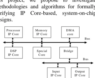
Hardware designs have reached a mammoth scale today, with over ten million transistors integrated on a single chip. This breakthrough in technology has, in fact, reached the point, where it is hard to design a complete system from scratch. Industry has already started designing a circuit from a large repertoire of Intellectual Property (IP) Components or IP Cores sold by many vendors. System-on-chip designs usually involve the integration of heterogeneous components on a standard bus as shown in Figure 1. Designers often do not have complete knowledge of the implementation details of each component. For example,
vendors may want to protect their IP Cores by only providing interface specifications. Consequently, the validation of such designs is becoming more and more challenging. In this project, we propose to investigate methodologies and algorithms for formally verifying IP Core-based, system-on-chip designs.
P roc essor IP Co re
Figure 1 A ty pical S OC desig n. M em o ry IP Co re D M A co re D SP IP Co re Spec ial C ore B rid ge In put IP Core O utp ut IP Co re B us B us
Figure 1 shows a typical IP Core based system using a collection of various IP cores, with interconnecting buses running among them. Since the cores may be obtained from different vendors, there is a need for standard buses to connect them. We also envision some kind of interface logic to connect IP Cores to the standard buses. In some cases IP Cores are designed to be compliant to a standard bus protocol and can be connected directly to the bus without glue. Bridges are used to extend such systems in a hierarchical fashion by connecting buses.
IP Cores are often pre-validated. This increases the confidence of system designer in third party IP Cores. The validation of IP Cores must be part of the IP Core design itself. So in this scenario, where we have a) pre-verified IP Cores with certain guarantees and confidence, b) a standard bus protocol, and c) IP Core specific glue to connect cores to the bus, we can decompose the task of verifying system-on-chip designs into three parts as follows:
1. Verify the interconnecting buses and bus bridges;
2. Verify the IP Core specific glue logic; 3. Given the verification guarantees of interconnecting buses and IP Cores, verify the
complete system.
Since the bus protocol is standard, it needs to be verified once and for all. Glue logic is IP Core specific. If we have a collection of protocols for IP Cores, then we can design an abstraction of the glue between the standard bus and each IP Core protocol. This abstract model is designed once. Then, we intend to check if the actual glue implementation refines the abstract model of the glue [7]. Thus, we have reduced the complexity of verifying the glue to checking refinement. When this is completed for all IP Cores and their glues, we can proceed to the third step.
Experience in industry with IP Core based ASIC designs shows that most of the bugs are found in the bus or glue logic. To our knowledge, there is still no agreement on a standard bus protocol for system-on-chip designs. However, the PCI Local Bus protocol [12, 13, 14] is widely accepted by many microprocessor based systems (eg. Pentium and Alpha) and IP Core companies. Therefore, we focus in this paper on verifying system-on-chip designs using the PCI Local Bus. This will provide insight into questions like, what basic functionality is required of the buses, what kind of standard interfaces are needed for IP Core based designs, and how glue logic may be designed and verified for heterogeneous IP Cores. We have formally verified the correctness of the PCI bus protocol using symbolic model checking [5].
In many cases, bus protocols can be verified with current for-mal verification techniques as demonstrated by [4] and [6]. We concentrate more on the functional properties of the PCI local bus and bridges rather than performance issues. A formal treatment of PCI bus performance is given by Campos, et al. in [4]. In a recent paper [11], theorem proving techniques have been used to validate a proposed solution for a bug in the PCI bus protocol, but this approach requires considerable expertise in modeling the bus and is not easily automated.
The increasing complexity and circuit size of designs have made function verification task as one of bottlenecks in VLSI design cycle. In recent conferences, many panelists claimed that functional verification takes about 60%-70% of design cycle.
The tasks of functional verification include detecting errors in designs and finding the causes of the errors (debugging process). To detect errors in designs, verification engineers and designers may generate test vectors manually, write test benches using tools, and write properties. Currently, formal verification tools checks whether the design satisfies their properties. If not, a set of counter-examples (``error traces'') can be generated to debug the design.
Usually, formal verification tools can generate good error traces to make the debugging process easier. Test vectors and test benches are mainly used in simulators and emulators to detect errors in designs. If errors are found, error traces are written out for debugging process. In general, these error traces produced by random/ pseudo-random test benches contain very long cycles and many redundant states. It is very difficult for users to debug using these traces and to take long simulation time to verify the bug fixes. Thus, we are inspired to develop the technique to compact error trace generated by random/pseudo-random test benches.
The main reason for compacting error traces generated by pseudo random simulations is that they may contains very long cycles and many redundant states. In the debugging process, users need to find the causes of bugs from the information in the error trace. Thus, The longer cycles of simulation trace are, the more time users spend to debug. Moreover, after finding the causes of bugs and fixing them, users perform the same simulation run to verify the bug fixes. Then, users put the simulation run into the daily regression suites to prevent the same bugs happen again. Therefore, shorter error traces not only reduce the simulation time required to verify bug fixes, but also reduce the simulation time for daily regression.
A digital circuit can be formulated as a finite state machine (FSM) and the circuit behavior can be viewed as the sequences of state traversal. The error trace contains all information of a sequence of state traversal from an initial state to an error state. The problem of compacting the error trace can be defined as follows: Given a digital circuit design and its simulation error trace information containing the initial state and the error state, the problem is to find other error trace as shorter as possible.
Our approach to solve compacting the error trace is based on the following three techniques: First, an efficient technique is used to eliminate the redundant states and to generate the unique states of the error trace. Then, the connected graph of these unique states is generated by computing the reachable states by one cycle for each unique state. The Dijkstra's shortest path algorithm is applied on the connected graph to find out the shortest error trace. Finally, the corresponding input/output test patterns are automatically generated for the new error trace. This algorithm is named as SET1. In experiments, we found out that not all of the unique states are needed to compute their reachable next states. Thus, algorithm SET2, modified from SET1, only computes the reachable states by one cycle for those unique states, when they are needed in Dijkstra's shortest path algorithm to find the shortest error trace.
四、結果與討論
We have implemented our SET1 and SET2 algorithms in C++ language with the CUDD (Colorado University Decision Diagram) package. The experiments were performed on a 1.4 GHz AMD Athlon machine with 2GB main memory.
Circuit CPU Time (sec) Mem (MB)
-Trace# SET1 SET2 Speedu
p SET1 SET2 B4-1 2847.40 183.58 15.5 12.28 11.79 B4-2 4882.02 933.54 5.2 17.47 16.65 B4-3 6864.21 1005.14 6.8 24.11 22.92 B4-4 8180.27 221.32 37.0 27.88 26.37 B4-5 8937.08 558.03 16.0 29.12 27.56
B11-2 272.43 153.58 1.8 92.18 51.38
Table 1. The results of SET1 and SET2.
Table 1 shows the CPU time and memory usage of SET1 and SET2 algorithms for cases in circuit ``b4'' and case ``b11-2'', which requires longer CPU times to find the shortest error trace. SET2 found the same length of shortest error trace as SET1 did. In general, SET2 used less memory usage to achieve the same quality as SET1 did, while SET2 improve the CPU time dramatically for cases in ``b4''. The CPU time improvement is contributed by that the number of states to compute the next states in SET2 is reduced from the number of unique states to the number states with length not greater than the length of the shortest error trace. For instance, in case ``b4-4'', SET1 compute the reachable next states for 9380 states, SET2 only compute the reachable next states for states with length less than 167 from initial state. Thus, SET2 has 37 times speedup than SET1 for this case.
We have published three papers based on this research work:
1. Jiunn-Chern Chen, Yirng-An Chen, "Equivalence Checking of Integer Multipliers", in Proceedings of ASP-DAC'01, 2001.
2. Chien-Pang Lu, Wen-Chien Liu, Yirng-An Chen,
“High Probability High Density Finite State Traversal”, in proceeding of IEEE/ ACM 10th International Workshop on Logic & Synthesis, 2001.
3. Yirng-An Chen, Fang-Sung Chen, “Algorithms for
Compacting Error Traces”, to be appeared in Proceedings of ASP-DAC'03, 2003
五、參考文獻
[1]. A. Aharon, D. Goodman, M. Levinger, Y Lichtenstein, Y. Malka, C. Metzger, M. Molco, G. Shurek, “Test Program Generation for Functional Verification of PowerPC Processors in IBM” In proceeding of ACM/IEEE Design Automation Conference 1995
[2] S. Berezin, A. Biere, E. Clarke, and Y. Zhu.
“Combining symbolic model checking with
uninterpreted functions”, In Proceeding of the Conference of Formal Methods in Computer Aided Design, Nov., 1998
[3] V. Bertacco, M. Damiani, S. Quer, “ Cycle-based symbolic simulation of gate-level synchronous circuits”, In Proceeding of the 36th Design Automation
Conference, June, 1999
[4] BROCK, B., KAUFMANN, M., AND MOORE, J.
S. “ACL2 theorems about commercial
microprocessors.” In Proceedings of the Formal Methods on Computer-Aided Design (November 1996), pp. 275-293.
[5] S. Campos, E. Clarke, W. Marrero, M. Minea. “Verifying the performance of the PCI Local Bus using Symbolic Techniques”, IEEE Intl. Conf. in Comp. Design, Oct. 1995.
[6] R. Chandramouli and S. Pateras, Testing Systems on a Chip," IEEE Spectrum, pp. 42-47, Nov. 1996. [7] P. Chauhan, E. Clarke, Y. Lu, D. Wang “Verifying IP-Core based System-On-Chip Designs”, IEEE Intl. Conf. in Comp. Design, Oct. 1999
[8] CLARKE, E. M., GERMAN, S. M., AND ZHAO, X. Verifying the SRT division using theorem proving techniques. In Computer-Aided Verification, CAV –96, Springer-Verlag, pp. 111-122.
[9] CLARKE, E.M., AND ZHAO, X. Analytica: A theorem prover for Mathematica. In The Journal of Mathematica (1993).
[10] L. Fournier, A. Koyfman, M. Levinger, “Developing an architecture validation suite – Application to the PowerPC architecture”, In Proceeding of the 33rd Design Automation Conference, June, 1999.
[11] R. Hosabettu, M. Sirvas, and G. Gopalakrishnan, “Decomposing the proof of correctness of pipelined microprocessors”, In Proceeding of the Computer Aided Verification Conference, June, 1998
[12] H. Iwashita, S. Kowatari, T. Nakata, F. Hirose “Automatic Test Program Generation for Pipelined Processors”, In Proceedings of the International Conference on Computer Aided Design, November 1994
[13] M. Kantrowitz and L.M. Noack, “ I’m Done Simulating: Now What? Verification Coverage Analysis and Correctness Checking of the DECchip 21164 Alpha Microprocessor”, In Proceeding of the 33rd Design Automation Conference, June, 1996. [14] MCMILLAN, K. L. Symbolic Model Checking. Kluwer Academic Publishers, 1993.
[15] K. McMillan, “ Verification of an implementation of Tomasulo’s algorithm by compositional model checking”, In Proceeding of the Computer Aided Verification Conference, June, 1998
[16] MCSORLEY, O. L. High-Speed arithmetic in binary computers. In Proceedings of IRE (1961), pp. 67-91.
[17] A. Mokkedem, R. Hosabettu, and G.
Gopalakrishnan. “Formalization and Proof of a Solution to the PCI 2.1 Bus Transaction Ordering Problem”, In Proceeding of the Conferenceof Formal Methods in Computer Aided Design, Nov., 1998 [18] J. Sawada, W. A. Hunt., “Processor verification with precise exceptions and speculative execution”, In Proceeding of the Computer Aided Verification Conference, June, 1998
[19] J. U. Skakkebak, R. B. Jones, D. L. Dill, “Formal verification of out-of-order execution using incremental flushing”, In Proceeding of the Computer Aided Verification Conference, June, 1998
[20] M. Velev, R. E. Bryant, “ Exploiting positive equality and partial non-consistency in the formal
verification of pipelined microprocessors”, In
Proceeding of the 36th Design Automation Conference, June, 1999.
[21] “VSI Alliance”, Architecture Document, version 1.0, 1997