1/
f
noise measurements on indium antimonide metal–oxide–semiconductor
field-effect transistors
U. H. Liaw and Y. K. Su
Department of Electrical Engineering, National Cheng Kung University, Tainan, Taiwan, Republic of China ~Received 20 July 1998; accepted for publication 5 March 1999!
We performed the 1/f noise measurements on n-channel indium antimonide~InSb! metal–oxide– semiconductor field-effect transistors~MOSFETs! biased in linear and saturation regions operated at 77 K. Through the investigation of the dependence of drain voltage noise power spectral density on gate and drain bias, we have estimated the oxide–semiconductor interface trap density as a function of energy. In this analysis, both the noise magnitude and the spectral shape were studied. In this study, the frequency span was performed from 150 Hz to 5 kHz. The noise behavior of the device was modeled using the modified McWhorter Model, originally developed for silicon FETs. The interface trap concentration values computed from the low-frequency noise measurements using the previous model were found to agree closely with InSb/SiO2 interface properties measured by capacitance and conductance methods. © 1999 American Institute of Physics.
@S0021-8979~99!05911-3#
INTRODUCTION
Indium antimonide ~InSb! is a direct, narrow band gap semiconductor which has important applications in infrared ~IR! radiation detection as charge transfer devices, linear and two-dimensional charge injection device arrays, and charge-coupled device imagers.1–3 As with other analog devices made of silicon or III–V semiconductors, InSb devices also suffer from excess 1/f noise. However, due to the relatively limited applications of this material, the noise properties of InSb devices have not been extensively studied as silicon devices have. Therefore, origin of 1/f noise in these InSb devices is still unknown and there are no theories to model their noise behavior. Moreover, when these devices are op-erated at low frequencies for IR radiation detection and sig-nal processing, 1/f noise usually dominates their operation.
Most of the experimental work on 1/f noise in silicon or III–IV, semiconductor devices has concentrated on p-n photodiodes.4–9 Although the value of band gap energy, as well as the type of surface passivation play important roles in the origin of excess noise, most researchers came to the com-mon conclusion that fluctuations in the generation-recombination ~G-R! current in the surface depletion region are responsible for the 1/f noise in these devices.4–6Among the theories to account for these fluctuations, the most popu-lar one has been the surface-trap induced-carrier fluctuation model that has been first introduced by McWhorter10 and later applied to p-n junctions by Hsu.11 It should be noted that 1/f noise fluctuations originating from the bulk depletion region have also been observed.7 In addition, bulk charge carrier mobility fluctuations,12 as well as Umklapp and co-herent state quantum fluctuations8,13 have been offered as models for the origin of 1/f noise in III–V semiconductor diodes.
Other investigations on excess noise of silicon and III–V semiconductor devices include photoconductors where the roles of grain boundaries and contacts on the magnitude of noise have also been examined.14–16However, to our
knowl-edge, there is no published work to date on the noise mea-surements and responsible mechanisms for InSb metal– oxide–semiconductor ~MOS! devices. Although one might be tempted to assume that the models developed for other metal–oxide-semiconductor field-effect transistor ~MOSFET! devices such as silicon and III–V semiconductor devices could be applied as well to InSb MOS devices, cau-tion should be exercised to include the unique material prop-erties of InSb such as its direct, narrow band gap and unique operation conditions of the IR devices, such as cryogenic temperatures and extreme low-noise requirements. Espe-cially, since the surface properties of InSb-dielectric inter-faces have not been extensively characterized, any surface noise model developed for Si–SiO2 should be applied with extreme care.
In this article, we present the results of 1/f noise mea-surements on InSb MOSFETs. In the next section, experi-mental procedures and results will be presented, followed by the detailed discussion of the results. Modified McWhorter model originally developed for MOSFETs will be applied to the experimental data with appropriate changes. InSb/SiO2 interface properties obtained through the fitting parameters of this model will be compared to the interface characteris-tics obtained by capacitance–voltage and conductance meth-ods.
EXPERIMENT
The MOSFETs on which the 1/f noise measurements were performed were fabricated in Texas Instruments on bulk InSb which corresponds to an energy band gap of 0.23 eV and a cut-off wavelength of 5.4mm at 77 K. The devices were n-channel and enhancement type. The p-type InSb sub-strates were Cd-doped with a background concentration of 331014cm23, while the n-type drain and source regions were obtained by doping with silicon to 831016cm23. The channel length was 25 mm, and the channel width varied between 25–75 mm. The surface was passivated with direct
8485
photo-chemical vapor deposition oxide followed by 1200 Å of SiO2 deposition as a gate dielectric.
1,3
The gate metal was chromium and gold with thicknesses of 300 and 800 Å, re-spectively.
A typical low-frequency noise measurement set-up, con-sisting of a PAR-113 preamplifier and a HP 3561 A dynamic signal analyzer, has been used. The details of the experimen-tal configuration can be found elsewhere.17The devices were loaded into a liquid N2double-jacket Dewar where they were cooled down to 77 K. All measurements were taken in dark. As with all noise measurements, a major concern in this experiment was the spurious noise sources. Since a shielded room was not available, special care had to be taken to mini-mize the extraneous noise sources in the laboratory. The double-jacket liquid nitrogen Dewar provided an adequate shield against most of the electrical radiation. The use of short BNC cables, metal-film resistors, and Al shielding boxes also helped to minimize the extraneous noise. More-over, the thermal noise of the device and the background noise were subtracted from the device noise measurements.
Depending on the purpose of the investigation, many ways to measure and express the excess noise of a MOSFET exists. The spectral density of drain-to-source voltage SVdor current SIdcan be measured. This can be referred to the input in the form gate-voltage noise SVg or expressed as output noise: SVd3SId. In our experiments, we chose to measure the drain-to-source voltage noise spectrum instead of drain current noise spectrum, since this is a direct way of observ-ing output noise without the use of an additional resistor. Furthermore, it is preferable to evaluate SVdinstead of SIdfor the simplicity of computations.17 The results were not con-verted to input gate noise, since it has been previously shown that this could lead to erroneous results at low drain voltages.18 However, this conversion can be easily done if needed.
The drain voltage noise power spectral density was mea-sured in the frequency range of 500 Hz–2 kHz. The lower frequency cut-off was chosen such that 60 Hz-line voltage and its first three harmonics were not visible in the measure-ments. The higher cutoff was set according to the levels of device thermal and background noise.
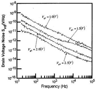
Figure 1 shows the typical noise spectra obtained at four different gate voltages of 1.0, 1.5, 2.0, and 2.5 V. The drain voltage was kept at a constant 0.2 V. Each spectrum corre-sponds to 1500 fast Fourier transform averages and follows a form of 1/fg where 0.7,g,1.1. Contrary to the noise ex-periments on silicon MOSFETs,17,19,20 we did not observe any dependence of g on either the gate bias or the drain voltage. The frequency exponent seemed to vary arbitrarily between the above limits, without following any trend. De-tailed discussion of this behavior will be done in the next section.
The gate voltage dependence of the noise power was investigated by measuring the drain voltage noise spectral density as a function of gate bias at a constant drain voltage of 0.2 V. The low-drain voltage was adopted for the ease of calculations and to avoid recombination-generation noise that is known to emerge at the drain end of the channel in the saturation region. Figure 2 depicts SVdat 500 Hz vs Vg at 77
K. The noise power decreases with increasing gate bias simi-lar to the trend observed in silicon MOSFETs, however, at a much slower pace. Similar behavior was noted for different frequencies and drain voltages. The data can be accounted for using modified McWhorter theory that will be explained in the next section.
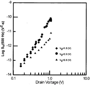
In addition to the gate voltage dependence, drain bias dependence of 1/f noise has also been studied with gate volt-age kept constant in the linear and saturation regions of op-eration. SVd( f5500 Hz) vs drain voltage is shown in Fig. 3 for the gate voltages of 1.5, 2.0, and 2.5 V. In the linear region of operation, the noise power consistently showed a clear Vd
3
dependence for all gate voltages. This is contrary to the predictions of the classical theory of resistance fluctua-tions where a quadratic dependence would be expected.17,20
FIG. 1. Typical noise spectra obtained at four different gate voltages of 1.0, 1.5, 2.0, and 2.5 V, respectively. The drain voltage was kept at a constant 0.2 V.
FIG. 2. The gate voltage dependence of the noise power at 500 Hz. The drain voltage was kept constant at 0.2 V. The line represents the theoretial curve fitted withj5210 ~eV21! and Ni5331019(cm23eV21).
At this point, we cannot fully account for this behavior. Some of the possibilities are the existence of contact noise— especially since the sample has a two-probe geometry which is inherently prone to contact noise—heating effects, or other anomalies.
In the next section, the experimental findings will be explained with a noise model developed for the linear opera-tion region of the MOSFETs. No attempt has been made to quantitatively analyze the saturation region data in this study.
THEORY AND DISCUSSION
In order to account for the data, modified McWhorter theory that has been originally developed for silicon surface-conduction devices such as MOSFETs was applied to InSb MOSFETs. According to this noise model, the responsible mechanism for 1/f noise is the fluctuations in the number of charge carriers due to trapping and detrapping of these car-riers by the surface states at the semiconductor-dielectric in-terface. The interaction between carriers and the trapping states in the dielectric occurs by tunneling at a constant en-ergy. The details of the model and the full derivation of the expression for the current noise power spectral density SI is given in previous articles.17,19 Here, only some aspects as they apply to the InSb MOSFETs are discussed.
As shown previously, in the linear region of transistor operation, the power spectral density for the drain current SId can be written as SI d5 2Wm2q2 L3 Vd~2Vds2Vd! 3
E
0 VdE
En EcE
d1 d2Nt~E,y!ft~E,V!@12 ft~E,V!#
3@11v2t2t~E,V,y!#~V~E,V,y! ds2V!
dy dE dV, ~1!
where W is the channel width,mis the mean electron mobil-ity in the channel, q is the elementary charge, L is the chan-nel length, Vds5Vg2VTis the drain saturation voltage, V(z)
is the potential at point z in the channel, Ecis the conduction band edge, En is the valence band edge, E is the trap energy level, Ntis the density of interface traps, ftis the occupancy of the traps,tis the tunneling time constant for the traps, y is the distance into the oxide, andv is the angular frequency. Using the elementary MOSFET theory and gradual channel approximation, an expression for the drain voltage noise power is obtained as SVd5
S
L WmCoVdsD
2 SId. ~2!Here, Co is the gate oxide capacitance.
Generally speaking, traps are distributed over space in-side the insulator, as well as in energy over the band gap. Any nonuniformity in the spatial distribution of the traps would cause a deviation in the shape of the pure 1/f power spectrum. For example, if there is a net increase in the trap concentration further in the insulator from the semiconductor interface, this would cause the carriers to encounter more traps as they tunnel into the insulator. Since the traps located further in the insulator correspond to higher time constants and therefore to lower frequencies, this would cause the noise power in the low frequency region of the spectrum to increase. Hence, the spectrum will be steeper than 1/f . In other words, the frequency exponent g in the 1/fg spectral form will be greater than one. Even if there is no intrinsic nonuniformity in the spatial distribution of the traps, band-bending due to gate bias will ‘‘pull down’’ the traps, effec-tively causing a nonuniform distribution relative to the car-riers tunneling at a constant energy. Consequently, a net increase or decrease in g will be observed with increasing gate bias depending on the energy distribution of the traps.19,20Since no such increase or decrease is observed in our experiment and gwas independent of gate bias, we as-sumed Nt to be only a function of energy E in our calcula-tions. Physically, the fact thatgis independent of bandbend-ing implies that in the range of gate bias we have performed our experiments, the Fermi level does not sweep a large en-ergy range such that the trap concentration does not change significantly. It might also imply that the interface trap den-sity remains constant in the whole band gap. The latter pos-sibility can be checked by the gate bias dependence of the 1/f noise magnitude. This point will be explained later in this section.
For our calculations, we assumed an exponential energy distribution of interface traps
Nt~E!5Niexp@j~E2Ei!#. ~3!
Here, Ni is the trap concentration at mid-gap, and jis the exponential factor. Negative, as well as positive values of j were considered. Negativejvalues correspond to an increas-ing trap concentration towards the mid-gap from the conduc-tion band-edge. Positive jvalues, on the other hand, corre-spond to the opposite trend. It should be noted that the factor ft(12 ft) in Eq.~1! ensures that the most significant contri-bution from the traps occurs in a narrow energy range. Therefore, any functional form of Nt can be chosen for that small energy range.17 We chose an exponential form for the ease of calculations.
FIG. 3. The drain voltage dependence of the noise power at 500 Hz for different gate biases.
Since the interface trap distribution does not depend on the distance y in the insulator, the inner integral with respect to y can be readily evaluated if t(E,V, y ) is known. The probability of penetration of the carriers in the insulator de-creases exponentially with distance from the interface, fol-lowing the Wentzel–Kramer–Brillouin approximation. Hence, the tunneling time constant tcan be expressed as21
t5t0exp~ay!. ~4! Although values for t0 and a are readily available for a Si–SiO2system, no such calculations have been done for the InSb–SiO2 interface. Here, we follow the approximate method used by Christensson, Lundstrom, and Svensson21to find afrom the barrier heightDE as
a54p
h
A
2m*DE, ~5!where, m* is the electron effective mass and h is Planck’s constant. The calculated a value of 33107 for InSb–SiO
2 interface is lower than that for Si–SiO2interface. Computing
t0, on the other hand, is harder, since the capture coefficient of surface-state traps at the InSb–SiO2 interface is still un-known. For our calculations we assumed a value of 1029s. This is reasonable in the light of other semiconductor inter-faces and agrees closely with the g-r relaxation times ob-served in InSb.22 If t0 is of the order of 1029s and a'4 3107cm21, for traps distributed up to 100 Å, the inner in-tegral of Eq.~1!
E
d1 d2 t11v2t2dy ~6!
can be approximated as p/2av for frequencies of 1026– 107Hz. This is a common approximation done in modeling 1/f noise in silicon devices. However, such short cuts are not apparent for InSb devices. All parameters have to be reevaluated. And all approximations that are routine for silicon devices have to be reconsidered.
The term ft(12 ft) in expression~1! behaves almost like a delta function around the quasi-Fermi level Fn for electrons.21 Therefore, the energy integral can be approxi-mated as
E
En EcNt~E!ft~12 ft!dE'4kTNt~Fn!ft~Fn!@12 ft~Fn!#. ~7! Here k is the Botzmann constant, and T is the temperature. Combining Eqs.~1!, ~2!, ~6!, and ~7!, one obtains the expres-sion for drain voltage noise power spectral density
SVd5 2q2kTN i Ci2LWaf Vd~2Vds2Vd! Vds2 3
E
0 Vd 1 ~Vds2V! exp@j~kTUs2qV/2!# 21exp@2~2Us2qV/kT!#2dV, ~8! where Us is the unitless measure of band-bending at the semiconductor-insulator interface defined as23Us5 1
kT
S
2Ei1~Fn1Fp!
2
D
. ~9!Here Fp is the quasi-Fermi level for holes. The exponential term in the denominator of the integral in Eq.~8! comes from the factor ft(12 ft) in Eq. ~7!, whereas the numerator is derived from the interface trap distribution
Nt~Fn!5Niexp@j~Fn2Ei!#5Niexp@j~kTUs2qV/2!#. ~10! The band-bending, Usis essentially the surface potential and therefore a function of the gate bias, as well as the chan-nel potential. This term can be evaluated for each Vg and V using conventional charge technique.23 Expression ~8! is a simple numerical integration with respect to channel voltage V. We used Simpson’s method to evaluate the integral for different gate and drain voltages.
There are two fitting parameters, namelyjand Ni, to fit the theory to the experimental findings. In our analysis, we first found the optimum value of j such that the computed change of noise spectral density with respect to gate bias agrees with the data. Then, the absolute magnitude of 1/f noise was fitted to the data by varying the trap concentration at mid-gap Ni. The calculated curve in Fig. 2 corresponds to
j5210 ~eV21! and Ni5331019(cm23eV21) and agrees very well with the measured values for the drain voltage of 0.2 V. The only discrepancy occurs at the lowest gate biases where the transistor is in saturation. Since the model is valid for the linear region of FET operation, this should be ex-pected. If the traps are distributed in the SiO2 layer up to a few angstroms, Ni value of 331019(cm23eV21) corre-sponds to an interface state density of 1011(cm22eV21) at mid-gap.
It should be noted, however, that at the bias conditions we operated the devices, the quasi-Fermi level for the elec-trons was at or above the conduction band edge, 0.10(eV) <(Fn2Ei)<0.15(eV). Therefore, the trap concentration values obtained from the fitting parameters are actually valid for that energy interval. The midgap interface state density Niis merely an extrapolation. Using the above values of Ni and j, one can extract the trap concentration for the above energy range from the measured gate bias dependence of noise magnitude. This is shown in Fig. 4. The computed interface trap density for the conduction band edge is 9 31010(cm22eV21) which is in close agreement with the values obtained by Yang et al. using capacitance and con-ductance methods.24Moreover, the general trend of increas-ing trap density from the conduction band edge towards the mid-gap, i.e., the negative j value in our model, has also been observed by the same researchers.
We also attempted to predict the drain voltage depen-dence of the power spectral density. As discussed previously, the model yields a quadratic dependence on drain voltage, whereas the measurements showed a clear Vd3 dependence for the linear region. The computed curve using the fitting parameters found from Fig. 2 is compared to the measured values for the gate bias of 2.0 V in Fig. 5.
As a last point to this section, we would like to discuss the effect of considering correlated carrier mobility
fluctua-tions in the model, as well as the carrier density fluctuafluctua-tions. The trapping centers in the semiconductor–oxide interface and in the dielectric may cause fluctuations in the mobility of the channel carriers through coulombic scattering by the fluctuating trapped charge in these centers.25 Since both the carrier number fluctuations and the mobility fluctuations are due to the trapping and detrapping events at the interface, they are correlated. Detailed derivation of the correlated model has been done by Jayaraman and Sodini,26 and inde-pendently by Hung et al.27 Given a measured level of 1/f noise, the extracted trap densities from the data are lower for the correlated model than the pure number fluctuation model. However, since the difference is small,26i.e., well within the same magnitude, in this study we did not attempt to include
mobility fluctuations in our model. The error introduced into the calculated trap density values due to this omission is well within the experimental error.
CONCLUSION
We have performed low-frequency noise measurements on InSb. MOSFETs at 77 K. The modified McWhorter theory originally developed for silicon MOSFETs is shown to give the correct dependence of 1/f noise spectral density on gate bias. However, contrary to the predicted quadratic dependence on the drain voltage, we have observed a Vd3 dependence in our measurements. We believe the increase in noise magnitude at high drain voltages is due to heating ef-fects. The interface trap distribution extracted from the mea-surements using the McWhorter model agrees closely with independent measurements on InSb MOS structures using capacitance and conductance techniques.
ACKNOWLEDGMENTS
This work was supported by the National Science Coun-cil and Chung Shan Institute of Science and Technology of the Republic of China under Contract No. NSC 85-2215-E150-006.
1Y. K. Su and U. H. Liaw, J. Appl. Phys. 76, 4719~1994!.
2S. L. Tu, K. F. Huag, and S. J. Yang, Jpn. J. Appl. Phys., Part 2 28, L1874
~1989;!.
3
Y. K. Su, C. J. Hwang, R. L. Leuand, and F. M. Pan, Solid-State Electron.
34, 107~1991!.
4P. Tobin, S. Lwasa, and T. J. Tredwell, IEEE Trans. Electron Devices
ED–27, 43~1980!.
5W. A. Radford and C. E. Jones, J. Vac. Sci. Technol. A 3, 183~1985!. 6
H. K. Chung, M. A. Rosenberg, and P. H. Zimmmermann, J. Vac. Sci. Technol. A 3, 189~1985!.
7J. Baja, G. M. Williams, N. H. Sheng, M. Hinnrichs, D. T. Cheung, J. P.
Rode, and W. E. Tennant, J. Vac. Sci. Technol. A 3, 192~1985!.
8
X. Wu, J. B. Anderson, and A. van der Ziel, IEEE Trans. Electron Devices
ED–34, 1971~1987!.
9W. W. Anderson and H. J. Hoffman, J. Vac. Sci. Technol. A 1, 1730
~1983!.
10A. L. McWhorter, Semiconductor Surface Physics~University of
Pennsyl-vania Press, Philadelphia, 1957!.
11S. T. Hsu, Solid-State Electron. 13, 843~1970!.
12T. G. M. Klienpenning, J. Vac. Sci. Technol. A 3, 176~1985!. 13P. H. Handel, in Noise in Physical Systems and 1/f Noise, edited by M.
Savelli, G Lecoy, and J. P. Nougier~Elsevier, New York, 1983!, p. 97.
14
H. I. Hanafi and A. van der Ziel, Solid-State Electron. 21, 1019~1978!.
15H. I. Hanafi and A. van der Ziel, Solid-State Electron. 21, 1019~1978!. 16H. I. Hanafi and A. van der Ziel, Physica B & C 94, 351~1978!. 17Z. Celik and T. Y. Hsiang, IEEE Trans. Electron Devices ED–32, 2797
~1985!.
18A. van der Ziel, H. S. Park, and S. T. Liu, Appl. Phys. Lett. 35, 942
~1979!.
19Z. Celik-Butler and T. Y. Hsiang, Phys. Rev. B 33, 4898~1986!. 20C. Surya and T. Y. Hsiang, Phys. Rev. 35, 6343~1987!. 21
S. Christensson, I. Lundstrom, and C. Svensson, Solid-State Electron. 11, 797~1968!.
22R. N. Sharma, Ph.D. thesis, University of Minnesota, 1969.
23J. W. Haslett and F. N. Trofimenkoff, Solid-State Electron. 15, 117
~1972!.
24
M. J. Yang, C. H. Yang, M. A. Kinch, and J. D. Beck, Appl. Phys. Lett.
54, 265~1989!.
25C. Surya and T. Y. Hsiang, Phys. Rev. 35, 6343~1987!.
26R. Jayaraman and C. G. Sodini, IEEE Trans. Electron Devices ED–36,
1773~1989!.
27K. Hung, P. Ko, C. Hu, and Y. Cheng, Tech. Dig. Int. Electron Devices
Meet.~1988!, p. 34. FIG. 4. Extracted trap density vs energy. The curve was obtained from the
fitting parameters and Niin Fig. 2.
FIG. 5. The computed drain voltage dependence of the noise power at 500 Hz is compared to the data obtained at the gate bias of 2.0 V. The same fitting parameters of j5210 ~eV21! and Ni5331019(cm23eV21) have