Buckling characterization of vertical ZnO nanowires using nanoindentation
Liang-Wen Jia兲
Institute of Electro-Optical and Materials Science, National Formosa University, Yunlin 632, Taiwan, Republic of China
Sheng-Joue Young
Institute of Microelectronics, National Cheng Kung University, Tainan 701, Taiwan, Republic of China and Department of Electrical Engineering, National Cheng Kung University, Tainan 701, Taiwan, Republic of China
Te-Hua Fang and Chien-Hung Liu
Institute of Electro-Optical and Materials Science, National Formosa University, Yunlin 632, Taiwan, Republic of China
共Received 3 August 2006; accepted 11 December 2006; published online 17 January 2007兲 Nanomechanical characterization of vertical well-aligned single-crystal ZnO nanowires on ZnO:Ga/ glass templates was performed by nanoindentation technique. The buckling loads were found to be 1465 and 215N for the ZnO nanowires of 100 and 30 nm diameters, respectively. Furthermore, the buckling energies for the ZnO nanowires of 100 and 30 nm diameters were 3.62⫻10−10and
3.69⫻10−11J, respectively. Based on the Euler buckling model, Young’s modulus of the individual
ZnO nanowire has been derived from two possible modes in this work. © 2007 American Institute of Physics. 关DOI:10.1063/1.2431785兴
One-dimensional 共1D兲 materials such as nanowires 共NWs兲, nanobelts, and nanorods have attracted considerable interest in recent years.1–3They present the utmost challenge to semiconductor technology, making possible fascinating novel devices. These 1D materials have been demonstrated to exhibit superior electrical, optical, mechanical, and ther-mal properties, and can be used as nanoscale interconnects, active components of optical electronic devices, and nano-electromechanical systems. However, it is important to un-derstand the mechanical characteristics of these nanowires prior to any feasible applications. For example, mechanical properties of carbon nanotubes have been extensively studied by tensile loading, bending, and buckling.2,3
1D oxide systems such as SnO2, SiO2, GeO2, indium tin
oxide, Al2O3, and ZnO nanowires have also attracted much attention in recent years.4–12Among them, ZnO is a n type direct-gap semiconductor with a large exciton binding energy of 60 meV and wide band gap energy of 3.37 eV at room temperature. Hence, ZnO is regarded as a promising photo-nic material.13However, only few reports on the mechanical properties of ZnO nanowires can be found in the literature.4–8In this work, the buckling instabilities in verti-cal ZnO NWs have been characterized by nanoindentation tests. Based on Euler buckling model, we also estimated Young’s modulus共elastic modulus兲 of individual NW.
The ZnO NWs used in this study were grown on ZnO:Ga/glass templates, the synthesis of NWs was per-formed by a modified self-catalyzed vapor-liquid-solid method without any metal catalyst.12Detailed growth proce-dures can be found elsewhere.9,10 The photoluminescence 共PL兲 and x-ray diffraction 共XRD兲 were then used to charac-terize the optical and crystallographic properties of the as-grown ZnO NWs. Surface morphologies of samples and size distribution of the NWs were characterized by a LEO 1530
field-emission scanning electron microscope共FESEM兲, oper-ated at 5 keV. The investigation on the buckling behavior of the NWs was performed by means of a Hysitron nanoinden-tation system. Uniaxial compression on the exposed NWs was accomplished with a diamond indenter of 2m diameter.
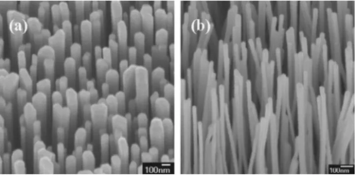
The FESEM images of the as-grown ZnO NWs in samples A and B were shown in Fig.1共a兲and1共b兲. We found the typical diameter, length, and density of the ZnO NWs in sample A were approximately 100 nm, 2000 nm, and 8.2 ⫻109cm−2while the ones of sample B were estimated to be
30 nm, 800 nm, and 1.2⫻1010cm−2, respectively. Note that
we can tune the oxygen stream during NW growth to obtain the different size of ZnO NWs. It was found that these ZnO NWs were distributed uniformly across the entire substrate and the tops of these NWs were hexagonal with the c axis perpendicular to the substrate surface.12 As shown in Fig. 1共a兲, the FESEM image reveals that some wires are stuck together for the 100-nm-diameter wires. For the 30-nm-diameter wires, the same phenomenon is observed, and the wires are also bending and not perfectly straight, as shown in Fig. 1共b兲. The stuck wires will cause smaller dis-placement than the single vertical wires under the same
load-a兲Author to whom correspondence should be addressed; electronic mail: [email protected] and [email protected]
FIG. 1. FESEM images of共a兲 sample A with the 100-nm-diameter ZnO NWs, and共b兲 sample B with the 30-nm-diameter ones.
APPLIED PHYSICS LETTERS 90, 033109共2007兲
0003-6951/2007/90共3兲/033109/3/$23.00 90, 033109-1 © 2007 American Institute of Physics
ing force. Furthermore, it will also result in higher critical buckling loads and Young’s modulus of the NW samples. From x-ray diffraction and photoluminescence measure-ments 共Fig.2兲, it was found that the ZnO nanowires were preferred oriented in the 共002兲 c axis direction with good crystal quality.
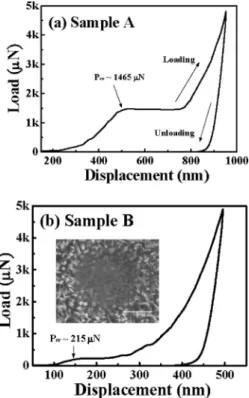
Samples A and B with the vertical ZnO NWs of 100 and 30 nm diameters were used in the nanoindentation tests. The NWs were loaded to a prescribed force and then unloaded in a force-controlled mode. Because each test was destructive in nature, several tests on different areas of the sample were conducted to check for repeatability. As shown in the inset of Fig.3, it can be seen that the distorted ZnO NWs共sample B兲 appeared after the nanoindentation experiments. Note that the opening angle of the conical indenter is estimated to 70°. We predict that the effect of opening angle could result in an increase of larger contact areas and higher critical buckling loads for NWs; therefore Young’s moduli will be evaluated slightly higher.
It is well known that the behavior of an ideal column and/or nanowire compressed by an axial load P can be sum-marized as follows: 共1兲 if P⬍ Pcr, the column is in stable
equilibrium in the straight position;共2兲 if P= Pcr, the column
is in a neutral equilibrium in either the straight or a slightly bent position; and共3兲 if P⬎ Pcr, the column is in unstable equilibrium in the straight position and will buckle under the slightest disturbance. Such a type of buckling is called Euler buckling.14 Figure3 shows load-displacement curves of the ZnO NW samples, in which each plot represents a loading-unloading cycle. The loading portion consists of three stages: an initial increase共P⬍ Pcr兲, followed by a sudden drop in the
slope and the curve becomes flat共P= Pcr兲, and a third stage
comprising an increasing load 共P⬎ Pcr兲. Where sample B
shows less contact force than sample A in the initial elastic regions of the load-displacement curves, the behavior of buckling instability is observed in the flat regions. Hence, the individual ZnO NW in this work can be regarded as an ideal column. The collapse force is 1465N for sample A, whereas it is 215N for sample B, as shown in Fig.3. The critical buckling loads of the ZnO NWs are therefore found to be 1465 and 215N for samples A and B, respectively. Furthermore, the buckling energies were 3.62⫻10−10 and
3.69⫻10−11J for samples A and B, respectively.
By the FESEM images of the buckled ZnO NWs in top view, as shown in the inset of Fig.3, we can easily estimate the average critical buckling loads of individual ZnO NW for samples A and B at about 5.68 and 0.57N, respectively. This value is important in determining Young’s modulus of a single ZnO NW.
The critical load for an ideal elastic column is often called the Euler load and is given by Pcr=2EI / Le
2
, where E is Young’s modulus and the moment of inertia is I =R4/ 4
for the column共vertical ZnO NW兲. The effective length Leis expressed in terms of an effective-length factor K: Le= KL, where L is the actual length of the column. The buckling behavior of ZnO NWs in this work can be approached by two possible conditions as follows:共1兲 K=0.5, a nanocolumn with both ends fixed against rotation is called a fixed-fixed column, where Pcr= 42EI / L2; 共2兲 K=0.7, a nanocolumn
fixed at the base and pinned at the top is called a fixed-pinned column, where Pcr= 2.0462EI / L2. For an Euler
buckling column, the critical buckling strain is given bycr
=cr/ E, where critical buckling stresscr= Pcr/ A.14
As shown in TableI, we can estimate critical stress共cr兲, critical buckling strain 共cr兲, and Young’s modulus 共E兲 of
ZnO NWs by critical buckling load of individual ZnO NW. It should be noted that the value of Young’s modulus for single-crystal ZnO bulk is 111.2 GPa,15and smaller than the values of ZnO NWs. Based on Euler buckling, it was found that Young’s modulus of ZnO NWs increases with decreas-ing diameter whether we evaluate the ones by fixed-fixed
FIG. 2. Room temperature PL spectra of the as-grown ZnO NWs共samples A and B兲. Inset exhibits XRD spectra for samples A and B.
FIG. 3. Force vs displacement curve of sample A共a兲 and sample B 共b兲. Inset shows a FESEM image of the buckled ZnO NWs共sample B兲 in top view.
TABLE I. Critical stress, critical buckling strain, and Young’s modulus of the ZnO NWs.
Sample description共length: L, diameter: D兲 cr 共MPa兲 K cr 共%兲 E 共GPa兲 A共ZnO NWs兲 L = 2000 nm, D = 100 nm 723 0.5 0.62 117 723 0.7 0.32 229 B共ZnO NWs兲 L = 800 nm, D = 30 nm 806 0.5 0.35 232 806 0.7 0.18 454
Single-crystal bulk wurtzite ZnO 111.2a
aReference15.
033109-2 Ji et al. Appl. Phys. Lett. 90, 033109共2007兲
column 共K=0.5兲 or fixed-pinned column 共K=0.7兲 mode. These results correspond with the work of molecular dynam-ics simulations performed by Kulkarni et al.,6as well as the experimental revelation of Chen et al.7This behavior can be attributed to high compressive internal stress levels resulting from the surface stress and high surface-to-volume ratios at the nanoscale.6,7 In other words, because our experimental NWs are high quality single crystals with few defects, it is expected that such a phenomenon of size dependence may originate from surface modification of NWs, as the surface effect becomes significant due to the large surface-to-volume ratio.
In summary, we report the experimental observations of buckling instabilities of vertical well-aligned single-crystal ZnO nanowires prepared on ZnO:Ga/glass templates. The critical buckling loads of the ZnO NWs are found to be 1465 and 215N for samples A共100 nm diameter兲 and B 共30 nm diameter兲, respectively. Furthermore, the buckling energy was 3.62⫻10−10 and 3.69⫻10−11J for samples A and B,
respectively. Euler buckling model can be employed in evaluating Young’s modulus 共E兲 and the critical buckling strain共cr兲 of individual ZnO NW.
This work was supported by National Science Council of Taiwan under Contract No. NSC-95-2221-E-150-077-MY3.
The authors would like to thank the Advanced Optoelec-tronic Technology Center, National Cheng Kung University, Taiwan for the support through equipment and cooperation.
1L. W. Ji, T. H. Fang, S. C. Hung, Y. K. Su, S. J. Chang, and R. W. Chuang, J. Vac. Sci. Technol. B 23, 2496共2005兲.
2P. Poncharal, Z. L. Wang, D. Ugarte, and W. A. de Heer, Science 283, 1513共1999兲.
3M. F. Yu, O. Lourie, M. J. Dyer, K. Moloni, T. F. Kelly, and R. S. Ruoff, Science 287, 637共2000兲.
4H. Saitoh, Y. Namioka, H. Sugata, and S. Ohshio, Jpn. J. Appl. Phys., Part 1 40, 6024共2001兲.
5S. X. Mao, M. H. Zhao, and Z. L. Wang, Appl. Phys. Lett. 83, 993共2003兲. 6A. J. Kulkarni, M. Zhou, and F. J. Ke, Nanotechnology 16, 2749共2005兲. 7C. Q. Chen, Y. Shi, Y. S. Zhang, J. Zhu, and Y. J. Yan, Phys. Rev. Lett. 96,
075505共2006兲.
8Z. L. Wang and J. H. Song, Science 312, 242共2006兲.
9V. Valcarcel, A. Souto, and F. Guitian, Adv. Mater.共Weinheim, Ger.兲 10, 138共1998兲.
10Z. W. Pan, Z. R. Dai, and Z. L. Wang, Science 291, 1947共2001兲. 11Z. R. Dai, Z. W. Pan, and Z. L. Wang, Adv. Funct. Mater. 13, 9共2003兲. 12C. L. Hsu, S. J. Chang, H. C. Hung, Y. R. Lin, C. J. Huang, Y. K. Tseng,
and I. C. Chen, IEEE Trans. Nanotechnol. 4, 649共2005兲.
13Z. X. Mei, X. L. Du, Y. Wang, M. J. Ying, Z. Q. Zeng, H. Zheng, J. F. Jia, Q. K. Xue, and Z. Zhang, Appl. Phys. Lett. 86, 112111共2005兲. 14S. P. Timoshenko and J. M. Gere, Theory of Elastic Stability
共McGraw-Hill, New York, 1961兲, p. 46.
15S. O. Kucheyev, J. E. Bradby, J. S. Williams, C. Jagadish, and M. V. Swain, Appl. Phys. Lett. 80, 956共2002兲.
033109-3 Ji et al. Appl. Phys. Lett. 90, 033109共2007兲