國立交通大學
材料科學與工程研究所
博士論文
增強型
磷化銦鎵/砷化鋁鎵/砷化銦鎵
假晶高電子遷移率電晶體之研究
研 究 生:褚立新
指導教授:張 翼 博士
中華民國九十六年一月
增強型磷化銦鎵/砷化鋁鎵/砷化銦鎵假晶高電子遷移率電晶
體之研究
The study of Enhancement-mode InGaP/AlGaAs/InGaAs
Pseudomorphic High Electron Mobility Transistor
研 究 生:褚立新 Student: Li-Hsin Chu 指導教授:張 翼 博士 Advisor: Dr. Edward Yi Chang
國立交通大學
材料科學與工程研究所
博士論文
A Dissertation
Submitted to Department of Materials Science and Engineering College of Engineering
National Chiao Tung University In Partial Fulfill of the Requirements
For the Degree of
Doctor of Philosophy in Engineering 2007
Hsinchu, Taiwan, Republic of China
增強型磷化銦鎵/砷化鋁鎵/砷化銦鎵假晶高電子遷移率電晶體之研究
研究生:褚立新 指導教授:張 翼 博士 國立交通大學材料科學與工程研究所 摘要 近年來無線通訊(wireless communication)科技日新月異,已為世界科技產業重 要之一環。無線通訊系統已由類比無線通訊進入數位無線通訊,同時數位無線通 訊系統是世界公認的無線通訊系統發展主力。本論文即在研究應用於數位無線通 訊系統之增強型砷化鎵高電子遷移率電晶體,以期提高其功能的相關元件及製程 技術。 在此論文中,由磷化銦鎵/砷化鋁鎵/砷化銦鎵 所組成的結構首次應用於製造 增強型的高電子遷移率元件。以磷化銦鎵/砷化鋁鎵/砷化銦鎵 所組成的結構取 代傳統結構可進一步提升元件的特性。此磷化銦鎵/砷化鋁鎵/砷化銦鎵 結構優 於傳統的磷化銦鎵/砷化銦鎵 有下列原因:第一, 砷化鋁鎵/砷化銦鎵 的導電 帶的不連續性比磷化銦鎵/砷化銦鎵 來的高,對於電子的侷限性會較佳,此現象 將可以增進元件的輸出功率。第二, 砷化鋁鎵/砷化銦鎵 的介面比磷化銦鎵/砷化 銦鎵 更平滑,因為在磷化銦鎵/砷化銦鎵 的介面砷原子及磷原子會有交互擴散 行為產生。此結果造成磷化銦鎵/砷化鋁鎵/砷化銦鎵 的高電子遷移率電晶體的0.5×160 μm2 元件展現出很低的0.3V knee voltage, 且當元件的偏壓在 VDS=2.5V 時,汲極電流為 375mA/mm(閘極電壓在 0.7V)和最大的轉導為 550mS/mm 。 此元件亦展現及優之高頻特性;截止頻率為60GHz 且 最大震盪頻率為 128GHz. 此增強型的磷化銦鎵/砷化鋁鎵/砷化銦鎵元件,在 2.4GHz 的頻率下亦展現很高 的輸出功率密度453mW/mm 及極高的線性增益 30.5 dB 。另外此增強型元件其 最大的功率增加效率為70%。 另 一 方 面 , 先 進 的 無 線 數 位 通 訊 系 統 , 例 Wide-band Code-Division Multiple-Access (W-CDMA), 需要元件擁有高效率、良好的線性度及低消耗電壓 等特性。因此,高效率且高線性度的增強型磷化銦鎵/砷化鋁鎵/砷化銦鎵元件極 有發展的必要性。元件能夠在低電壓下操作必須有極低的knee voltage ;線性度 方面的改善,則需源自雙載子摻雜濃度的最佳化。本論文所製作之元件,當元件 偏壓在VDS = 2V 時,最大轉導值為 448 mS/mm。 在 10 GHz 的頻率下,其最低
雜訊指數為 0.86 dB 且增益為 12.21 dB 。此元件的 high output third order intercept point (OIP3)-P1dB 為 13.2 dB ,且在 WCDMA 的調變訊號下有著極高的
功率增加效率35%。
另外,此論文也探討利用鉑作為蕭基接觸金屬的增強型的磷化銦鎵/砷化鋁 鎵/砷化銦鎵元件。在依序濺鍍鉑/鈦/鉑/金為閘極金屬後,在 325 ℃ 下做退火處 理,使得閘極金屬擴散下沈。退火後,元件的 threshold voltage (Vth) 自 0.17V 正
上的改善源自於Schottky barrier height 的增高;在退火後,因為鉑擴散下沈的製 程,使得閘極至通道的距離減低。而且threshold voltage 的偏移非常均勻且具有 相當高的再現性,並且在退火後,元件有著更好的RF 功率特性。 最後,鉑金屬與磷化銦鎵 的界面反應也在此論文中討論。在濺鍍鉑金屬後, 會有著約 7.5nm 厚的非晶系層存在。由穿透式電子顯微鏡的影像顯示,在 325℃ 下經過一分鐘的退火後,鉑 金屬會往磷化銦鎵層擴散至約 12.8nm 。且在 325℃ 下,經過十分鐘的退火後,成核現象開始於磷化銦鎵層中產生。另外,在相同溫 度下,經過三小時的退火,即可發現新的相 Ga2Pt (422) 及 GaPt3 (422) 生成在 鉑及磷化銦鎵的介面中。
The study of Enhancement-mode InGaP/AlGaAs/InGaAs Pseudomorphic High Electron Mobility Transistor
Student: Li Hsin Chu Advisor: Dr. Edward Yi Chang Department of Materials Science and Engineering
National Chiao Tung University
Abstract
In recent years, digital wireless communication technology develops rapidly around the world. It is believed that the digital wireless technologies are the major trends for the future wireless communication systems. The purpose of this dissertation is to develop the Enhancement-mode high-electron-mobility transistor (HEMT) for the digital wireless communication systems with improved device structures and the related process technologies.
In this dissertation, the InGaP/AlGaAs/InGaAs structure was used to fabricate the enhancement-mode high-electron-mobility transistors with the goal of further enhancement of the HEMT device performance. The attempt on using the InGaP/AlGaAs/InGaAs heterojunction instead of the InGaP/InGaAs is due to: Firstly, the conduction band discontinuity of the AlGaAs/InGaAs interface is superior to those form at the InGaP/InGaAs interface, the carrier confinement would be better.
the interface between the AlGaAs/InGaAs interface is smoother than the InGaP/InGaAs interface due to the interdiffusion behavior of As and P atoms in the InGaP/InGaAs interface. As a result, the electron mobility of the InGaP/AlGaAs/InGaAs PHEMTs is higher than the electron mobility of the InGaP/InGaAs PHEMTs. The fabricated InGaP/AlGaAs/InGaAs HEMT 0.5×160 μm2
device shows low knee voltage of 0.3V, a high drain-source current (IDS) of
375mA/mm and a maximum transconductance of 550mS/mm when drain-source voltage (VDS) was bias at 2.5V. High-frequency performance was also evaluated; the
cut-off frequency (Ft) was 60GHz and the maximum oscillation frequency (Fmax) was
128GHz. The E-mode InGaP/AlGaAs/InGaAs PHEMT also exhibited high output power density of 453mW/mm with high linear gain of 30.5dB at 2.4GHz. The maximum power-added-efficiency (PAE) of the device was 70%, when tuned for the maximum power added efficiency.
On the other hand, advanced digital wireless application systems, such as Wide-band Code-Division Multiple-Access (W-CDMA) system, has imposed stringent requirements on the devices while include high efficiency and high linearity operation with minimum DC power consumption
.
Thus, a high linearity and high efficiency Enhancement-mode InGaP/AlGaAs/InGaAs PHEMT has to be developed. The low voltage operation is achieved by the very low knee voltage of the device andthe linearity is improved by optimizing the concentrations of the two delta-doped layers. Biased at a drain-to-source voltage VDS = 2V, the fabricated device exhibited a
maximum transconductance of 448 mS/mm. The measured minimum noise figure (NFmin) was 0.86 dB with 12.21 dB associated gain at 10 GHz. The device shows a
high output third order intercept point (OIP3)-P1dB of 13.2 dB and a high power
efficiency of 35% when under wideband code-division multiple-access (W-CDMA) modulation signal.
In addition, an Enhancement-mode InGaP/AlGaAs/InGaAs PHEMT using Platinum (Pt) as the Schottky contact metal was investigated for the first time. Following the Pt/Ti/Pt/Au gate metal deposition, the devices were thermally annealed at 325 for gate sinking. After the annealing, the device showed a positive threshold ℃ voltage (Vth) shift from 0.17V to 0.41V, and a very low drain leakage current of
0.16μA/mm which was reduced from 1.56μA/mm before gate sinking. These improvements are attributed to the Schottky barrier height increase and the decrease of the gate to channel distance as Pt sink into the InGaP Schottky layer during gate sinking process. The shift in the Vth was very uniform across a four inch wafer and
was reproducible from wafer to wafer. The device also showed excellent RF power performance after the gate sinking process.
in a Schottky diode structure. There was a 7.5 nm-thick amorphous layer formed at the interface between Pt and InGaP after metal deposition. After annealing at 325 ℃ for one minute, this amorphous layer increased to 12.8 nm and the reverse leakage current also decreased. The diffusion of Pt atoms and crystallization of amorphous layer took place after annealing at 325℃ for 10 minutes. Prolonging the annealing to 3 hours led to formation of Ga2Pt and GaPt3 phases in InGaP and Schottky diodes
誌謝
本論文能夠如期的完成,要感謝許多人的幫忙。首先要感謝我的指導教授張 翼博士,在我博士班的研究生活當中,不但帶領我進入砷化鎵高頻元件的領域, 提供完整的訓練及儀器資源,使我能夠參與建立實驗室高電子遷移率子電晶體製 程及相關量測設備建立。同時在待人處事和生活態度上,也給予很多寶貴的建 議,使我這幾年的求學生涯有著美好及愉快的回憶。 其次我要感謝李承士學長、陳仕鴻學長、張晃崇學長、王聖評學長在元件製 程上提供寶貴的經驗,使我利用正確且有效率的方法,去完成我的實驗。另一方 面,許恆通博士及研究員 李哲倫先生在電性量測上所提供的精闢的建議,也使 我獲益良多,而吳岳漢學弟在材料分析上的幫助,使得我的論文能夠以更完整的 形式呈現。 在研究生涯中,張尚文學長、連亦中同學、李晃銘同學、謝炎章同學在實驗 上的建議及生活上的扶持,是我最難忘的回憶。另外我要感謝曾孟修學長、何吉 真學姐、顧成芳學長、游智仲學長、黃瑞乾同學、陳克弦同學、張羅橫同學、徐 金鈺同學、沈伯村同學、吳偉成同學、張家源同學、郭建憶同學、彭怡瑄同學、 呂宗育同學、曾建堯同學、黃珍樺同學、吳玓雯同學、胡盈竹同學、林美璇同學、 唐士軒同學、詹前璋先生等,對於大家對我的協助與關懷致上最深的謝意。這幾 年,當我遇到挫折時,如果沒有曾士峰同學、陳昱嘉同學、尤似錦同學,還有安 亭一直給我的鼓勵與支持,我無法順利的完成學業,謝謝你們。 最後,我要特別感謝我的父母親,感謝你們的關心、支持、包容與鼓勵,使 我無後顧之憂,能夠專心順利完成學業,願這份榮耀與您們分享。Contents
Abstract (in Chinese)---I
Abstract (in English)--- IV
Acknowledge (in Chinese)--- VIII
Table Captions---XII
Figure Captions---XIII
Chapter 1 Introduction
1-1 GaAs Material Propriety---1
1-2 Pseudomorphic HEMT---2
1-3 Enhancement-mode Pseudomorphic HEMT---3
1-4 Outline of the Dissertation---4
Chapter 2 Fabrication of Pseudomorphic HEMT
2-1 Introduction---112-2 Device Isolation---14
2-3 Ohmic contact---15
2-4 Gate formation---19
2-5 Device passivation---22
2-6 Planting and Bridge interconnection---23
2-7 Back- side process---24
Chapter 3 Device Characterization
3-1 DC Characteristics---493-2 Scattering Parameters---51
3-3 Ft and Fmax---54
3-4 Noise Figure---55
3-5 Power and Power Added Efficiency---58
Chapter 4 Enhancement-mode InGaP/AlGaAs/InGaAs PHEMT
4-1 Introduction---724-2 Device Structure and Fabrication---74
4-3 DC Characteristics---75
4-4 RF Performance---76
4-5 Power Performance---76
4-6 Summary---78
Chapter 5 Double δ-Doped Enhancement-Mode Pseudomorphic
HEMT for high Linearity Application
5-1 Introduction---905-2 Device Structure and Fabrication---91
5-3 DC and RF Performance---92
5-4 Third-Order Inter-Modulation istortion---93
5-5 Wideband Code-Division Multiple-Access Power Performance---94
5-6 Summary---95
Chapter 6 Effect of gate sinking on the device performance of the
InGaP/AlGaAs/InGaAs E-mode PHEMT
6-1 Introduction---106
6-2 Device Structure and Fabrication---107
6-3 Gate sinking process and Schottky Characteristics---109
6-4 DC Characteristics---110
6-5 RF and Power Performance---111
6-6 Summary---112
Chapter 7 Interfacial reactions of Pt-based Schottky contacts on
InGaP
7-1 Introduction---1207-2 Schottky Diodes Fabrication---121
7-3 Experiment Results and Discussions---123
7-4 Summary---126
Chapter 8 Conclusions
---133Reference
---136Vita (in Chinese)
---146Table Captions
Chapter 1
Table 1-1 Advantages of GaAs HEMT ---8
Chapter 2
Table 2-1 Selectivity by using different solutions with various x values of the GaAs/AlxGa1-xAs structures. ---26
Chapter 3
Table 3-1 The most frequency used RF parameters for device haracterization[10]-61 Table 3-2 The y and h parameters in terms of the S-parameters[10].---62
Chapter 4
Table 4-1 2DEG sheet carrier concentration and mobility for the PHEMT structure [22]---79 Table 4-2 The electron mobility of InGaP/AlGaAs/InGaAs PHEMT and
InGaP/InGaAs PHEMT---80
Chapter 5
Table 5-1 Comparison of two tone output power performance for the two different structures.---99
Figure Captions
Chapter 1
Figure 1-1 The structure of the low noise Pseudomorphic AlGaAs/InGaAs HEMT ---9 Figure 1-2 The energy band diagram of the E-PHEMT with no bias applied [6]---10 Figure 1-3 The band diagram of the E-PHEMT at three different gate voltages
[6].---10
Chapter 2
Figure 2-1 Schematic of the cross section of the conventional HEMT [3].---27 Figure 2-2 The energy-band diagram of the conventional HEMT [3].---28 Figure 2-3 Lattice constant versus band-gap for III-V materials[3].---29 Figure 2-4 Schematic of the lattice of the Pseudomorphic HEMT structure [3].----29 Figure 2-5 The comparison of the structure and the band diagram of conventional HEMT and Pseudomorphic HEMT [3].---30 Figure 2-6 Schematic of the device layout.---31 Figure 2-7 The ideal mesa edge profiles produced on (100) GaAs surfaces using HF solution.---32
Figure 2-8 The test key for device isolation.---33
Figure 2-9 Device isolation I-V characteristic.---33
Figure 2-10 Band diagram for an idealized ohmic contact for a metal –N type-semiconductor junction (a) before contact and (b) after contact[9].---34
Figure 2-11 Ideal energy-band diagram of a metal- n type semiconductor ohmic contact. (a) with a positive voltage applied to the metal and (b) with a positive voltage applied to the semiconductor[9].---34
Figure 2-12 Energy band diagram of a heavily doped n-semiconductor to metal junction[9].---35
Figure 2-13 Alloyed AuGe/Ni/Au contacts, showing typical patterns if (a) under-alloyed; (b) alloyed correctly; (c) over-alloyed.---36
Figure 2-14 Ohmic contacts are separated by increasing distances.---36
Figure 2-15 Plot of measured resistance as a function of contact separation.---37
Figure 2-16 Plot of the contact resistance as a function of alloy temperature.---38
Figure 2-17 Process flow of the T-shape gate using Deep-UV aligner.---39
Figure 2-18 SEM image of the 0.5μm tri-layer T-shaped gate.---40
Figure 2-19 Process flow of the bi-layer T-shaped gate.---41
Figure 2-21 Saturation current before gate recess, after gate recess, and after gate
metallization [1].---42
Figure 2-22 The test key for the current monitor after recess etch.---42
Figure 2-23 The comparison of single and double recess process.---43
Figure 2-24 The SEM image of the device after Si3N4 deposition.---44
Figure 2-25 Dependence of the refracting index of a PECVD silicon nitride film on the of SiH4 flow rate.---45
Figure 2-26 SEM images of a plated air bridge structure.---46
Figure 2-27 Major steps in air bridge process.---46
Figure 2-28 Typical back-side process flow chart for HEMTs.---47
Figure 2-29 Schematic Cross section view of the metallized via-hole.---48
Chapter 3
Figure 3-1 Current-Voltage characteristics of the 0.25 μm × 160μm D-mode AlGaAs/InGaAs PHEMT.---63Figure 3-2 Transconductance and drain-source current vs. VGS of the 0.5 μm × 160μm D-mode PHEMT.---64
Figure 3-3 Gate-to-drain breakdown voltage. Specifying the gate-to-drain current is 1mA/mm.---65
Figure 3-4 S-parameters definition Schematic [10].---65
Figure 3-5 Typical H21, MAG/MSG and U as a function of the frequency for the 0.25μm × 160μm D-mode PHEMT when biased at VDS = 2V and VGS = -0.5V.---66
Figure 3-6 A generalized block diagram of a typical noise figure setup used to obtain noise parameters.---67
Figure 3-7 Noise performance of a 0.25μm D-mode PHEMT.---68
Figure 3-8 NF and Associated gain vs. Drain current for the PHEMT.---68
Figure 3-9 The power contours of a 0.25μm D-mode PHEMT.---69
Figure 3-10 Typical test equipment configuration used to make traditional load-pull measurement.---70
Figure 3-11 Typical power, Gain and Power added efficiency performance of a power HEMT device.---71
Chapter 4
Figure 4-1 Schematic showing the reactions and products between the InGaP/InGaAs layers during the growth.---81Figure 4-2 Device structure of the Enhancement mode InGaP/AlGaAs/InGaAs PHEMT.---82
Figure 4-3 I-V characteristics of the 0.5 μm × 160μm E-mode InGaP/AlGaAs /InGaAs PHEMT .---83 Figure 4-4 Transconductance and drain-source current vs. VGS of the 0.5 μm ×
160μm E-mode PHEMT.---84 Figure 4-5 The gate-to-drain breakdown voltage of E-mode PHEMT.---85 Figure 4-6 Distribution of Vth for E-mode PHEMT across 4 inch wafer.---85
Figure 4-7 Typical H21, MAG/MSG, as a function of the frequency for the 0.5 μm ×
160μm E-mode PHEMT biased at VDS = 2.5V and VGS = 0.5V.---86
Figure 4-8 Noise Figure and associated gain as a function of frequency at VDS = 2V
and IDS = 10 mA of the 0.5 μm × 160 μm E-mode PHEMT.---87
Figure 4-9 2.4 GHz power performance as a function of the input power for the 0.5 μm × 160μm E-mode PHEMT. (a) VDS=2V, VGS=0.2V. The device was
tuned for maximum power added efficiency. (b) VDS=2V, VGS=0.4V.
The device was tuned for maximum output power.---88 Figure 4-10 6 GHz power performance as a function of the input power for the 0.5 μm × 160μm E-mode PHEMT. (a) VDS=2V, VGS=0.2V. The device was
tuned for maximum power added efficiency. (b) VDS=2V, VGS=0.4V.
Chapter 5
Figure 5-1 The structure of E-mode InGaP/AlGaAs/InGaAs PHEMT. Upper Si δ-doping: 4.5×1012cm-2 (structure A) and 3.5×1012cm-2 (structure B).
Lower Si δ-doping : 1×1012cm-2.---100
Figure 5-2 Transconductance and drain-source current vs. VGS for the 0.5 × 200
μm2 E-mode PHEMT.---101
Figure 5-3 Noise Figure and associated gain as a function of frequency at VDS = 2V
and IDS = 10 mA of the 0.5 μm × 200 μm E-mode PHEMT.---102
Figure 5-4 The harmonic distortion plot[31].---103 Figure 5-5 The second order intermodulation distortion plot[31].---103 Figure 5-6 Pout (fundamental) and Pout (third order product) as a function of
Pin[31].---104
Figure 5-7 1.95 GHz one tone power performance as a function of the input power for the 0.5 μm × 200μm E-mode PHEMT. The device was tuned for maximum output power match.---105 Figure 5-8 Two tone output power and the third order products against input power. The device was biased at VDS=2 V, IDS=10 mA and tuned for maximum
Chapter 6
Figure 6-1 (a) The positions of the gate metal foot before and after annealing
(b)The cross-sectional TEM image of the as deposited Pt/InGaP interface
(c)The cross-sectional TEM image of Pt/InGaP interface after 325 ℃ annealing for 1min.---114
Figure 6-2 I-V characteristics of the diodes before and after annealing.---115 Figure 6-3 X–ray diffraction spectra of the Pt/Ti/Pt/Au and InGaP/AlGaAs/InGaAs PHMET sample before and after annealing at 325 for 3 hours. Main ℃ component: Ti, Pt, Au, Ga2Pt (JCPDS PDF 44-1288, 04-0802, 04-0784,
03-1007)---116 Figure 6-4 The transconductance and the drain-source current vs. VGS curves of the
0.7 μm × 240 μm E-mode PHEMT at VDS = 2V with 20nm thick Pt
before and after gate sinking at 325 for 1 min.℃ ---117 Figure 6-5 Threshold voltage of the Pt/Ti/Pt/Au E-mode PHEMT vs. annealing time when annealed at 325℃.---118 Figure 6-6 Distribution of Vth for the E-mode PHEMT across 4 inch wafer for two
different wafers.---118 Figure 6-7 (a)Power performance and gate leakage current of the 0.7 μm × 240μm
E-mode PHEMT before gate sinking (b) Power performance and gate leakage current of the 0.7 μm × 240μm E-mode PHEMT after gate sinking---119
Chapter 7
Figure 7-1 The HRTEM image of InGaP/Pt/Ti/Pt/Au.---127 Figure 7-2 (a) The cross-sectional HRTEM image of Pt and InGaP interface after metal deposition.(b) The cross-sectional HRTEM image of the Pt and InGaP interface after annealing at 325 for 1℃ minute.---128 Figure 7-3 (a) The cross-sectional HRTEM image of the Pt and InGaP interface
after annealing at 325 for 1℃ 0 minutes. (b) The Fast Fourier transform (FFT) lattice image of the amorphous area which was shown in Figure 2(a). The nucleation area was labeled by white square. (c) Nano –beam selected area electron diffraction pattern of the amorphous area shown in Figure 2(a).---129 Figure 7-4 (a) The cross-sectional HRTEM image of Pt and InGaP interface after 325 for 3 hours℃ annealing. (b) Nano-beam selected area diffraction pattern of Ga2Pt (422).---130
325 for 3 hours℃ annealing. (b) Nano-beam selected area diffraction pattern of GaPt3 (422).---131
Figure 7-6 I-V characteristics of the Schottky diodes before and after annealing. ---132
Chapter 1
Introduction
1-1 GaAs Material Propriety
Gallium arsenide is an III-V compound semiconductor; it is composed of Ga from column III of the periodic chart and As from the column V of the periodic chart. GaAs has some electronic properties which are superior to silicon's. It has a higher saturated electron velocity and a higher electron mobility which means that electrons can move faster in GaAs than in silicon, therefore, GaAs devices can operate at frequencies in excess of 250 GHz. Also, GaAs devices generate less noise than silicon devices when operated at high frequencies. GaAs devices also have higher power efficiency than Si devices when used as the devices.
The second major advantage of GaAs over silicon is the availability of the semi-insulating substrates. Silicon substrate generally can be made with resistivities above 100 Ω-cm. However, GaAs can be made with resistivities of 108Ω-cm.
Therefore, the GaAs makes device isolation easier. The semi-insulating GaAs substrate greatly reduces parasitic capacitance and provides an ideal substrate on which to fabricate microwave monolithic integrated circuits.
direct band-gap semiconductor, which means that it can be used to emit light. Silicon is an indirect band-gap material can not be used as light emitting material (Nonetheless, recent advances may make silicon LEDs and lasers possible). These properties make GaAs applicable to mobile phone, satellite communication, microwave point-to-point link systems as well as optoelectronics applications. [1]- [4]
1-2 Pseudomorphic High Electron Mobility Transistor
Since the first AlGaAs/GaAs conventional high electron mobility transistor (HEMT) was introduced in 1980 [5], many researchers working on high frequency devices have gradually moved toward HEMT technology. HEMT technology is compelling because it provides improved carrier transport characteristics in the channel, and enhances the performance of the devices at higher frequencies.
Moreover, the adventages of molecular beam epitaxy (MBE) and metal-organic chemical vapor disposition (MOCVD) has improved the capability of composition, doping concentration and thickness control of the epitaxial materials. As a consequence, high quality epitaxial structures are realized for the design and development of the advanced high performance device structures. The research for realized the high performance device technology has moved HEMT structure from the conventional AlGaAs/GaAs material to more advanced Pseudomorphic
AlGaAs/InGaAs system due to the latter has higher electron mobility and current density. The AlGaAs/InGaAs Pseudomorphic HEMT is shown in Figure 1-1.
1-3 Enhancement-mode Pseudomorphic HEMT
The key advantage of Enhancement-mode Pseudomorphic HEMT (E-PHEMT) when used for wireless applications is that it can operate with a single positive voltage source. Ordinary depletion-mode PHEMTs conduct current at zero gate bias, or the drain current reaches a saturated level (Idss) when the applied gate voltage is zero volt. An E-PHEMT exhibited no conduction (zero current) at zero gate bias, so that Id=0 at Vgs =0V. Therefore, it can operate without the negative voltage required for the
depletion-mode devices.
The energy band diagram for the E-PHEMT is as shown in Figure 1-2. At zero gate bias, the E-PHEMT structure is essentially fully depleted of conduction electron due to the conduction band is above the Fermi level. Therefore, the E-PHEMTs only require positive gate bias voltage for operation, and can be turned off with zero volts on the gate. Figure 1-3 illustrates how the electrons overcome the energy barriers with forward bias Vg. The dotted circles show where electrons accumulated. Below
threshold (Vg < Vth), minor conduction occurs in the lower n-AlGaAs layer where the
turn-on (Vth<Vg<VF), conduction occurs principally through the 2-DEG. At voltages
above turn-on (Vg>VF), the n-AlGaAs supply layer dips below Efn and conduction
transfers form the InGaAs 2-DEG to the n-AlGaAs layer and ,thus, the forward gate bias is limited by VF [6]. Hence, the gate leakage current will dramatically increase
when the forward gate bias is over VF.
1-4 Outline of the Dissertation
In this dissertation, high performance Enhancement-mode InGaP/AlGaAs/InGaAs Pseudomorphic High electron mobility transistor with low noise figure, high gain, high power added efficiency (PAE) and high linearity operated at low bias voltage are realized for wireless communication system applications.
The brief descriptions of basic HEMT process and device characteristics are given in Chapter 2. Due to the devices are for millimeter wave application, sub-micro T-shape gates are required in this study and are realized by using e-beam lithography and Deep UV light. By using e-beam writer and bi-layer photo resist, the 0.15μm gate length was developed. Also, in Chapter 3, the basic introductions of the DC and RF parameter for Low noise and power device are given. In addition, the power measurement system is also present.
PHEMT characteristics. In this study, the InGaP/AlGaAs/InGaAs PHEMTs instead of InGaP/InGaAs PHMETs are developed to further enhance the device performance. The attempt on using the InGaP/AlGaAs/InGaAs heterojunction instead of the InGaP/InGaAs is due to: Firstly, the conduction band discontinuity of the AlGaAs/InGaAs interface is superior to the InGaP/InGaAs, the carrier confinement would be better. This will improve the output power performance of the InGaP PHEMTs. Secondly, the interface between the AlGaAs/InGaAs interface is smoother than the InGaP/InGaAs interface due to the inter-diffusion behavior of As and P atoms in the InGaP/InGaAs interface.
Chapter 5 demonstrates a double delta-doped InGaP/AlGaAs/InGaAs E-mode PHEMT device capable of achieving low noise, high power efficiency, and high linearity with single voltage supply. For advanced high performance wireless application systems, such as Wide-band Code-Division Multiple-Access (W-CDMA) system, have imposed stringent requirements on the devices which include high power efficiency and high linearity operation with minimum DC power consumption. Conventional approaches in realizing both high linearity and high power simultaneously involve operating the power device at an output power level backed off from P1dB by about 6 dB. In that sense, the efficiency at the operating power level
turn consumes substantial system DC power. With low voltage operation achieved by the very low knee voltage of the device, the linearity is improved by optimal channel thickness and the use of double delta doping. This state-of-the-art device features a high PAE of 35% at maximum linear output power of 9.28 dBm under W-CDMA modulation.
Chapter 6 discusses the gate sinking effect of InGaP/AlGaAs/InGaAs E-mode PHEMT device with Pt/Ti/Pt/Au gate metals. The results show that Pt sinking is the dominant degradation mechanism. Pt sinking is caused by Pt diffusion into the InGaP Schottky barrier layer. Pt sinking explains the observed evolutions of the Schottky characteristics, Ids and gm transfer characteristic, and the S21 increase. Therefore, it is
important to fully understand the gate sinking process techniques in order to further improve the reliability of the E-PHEMT devices.
In chapter 7, the interfacial reactions between Pt and InGaP are studied. Traditionally, the Ti/Pt/Au metals are used as Schottky contact metals on the InGaP layer. Although, the Pt exhibited a high Schottky barrier height on InGaP which can reduce the leakage current, but there are few reports using Pt/Ti/Pt/Au as the Schottky contact metals on InGaP. In the past few years, Pt/InP and Pt/GaAs interfacial reactions had been reported. After thermal annealing, both Pt-In phase and PtP2 are
after the Pt and GaAs interfacial reaction. However, there are few reports investigating Pt and InGaP interfacial reactions; therefore the material analysis and current-voltage characterization are carried out to investigate the interactions between Pt and the InGaP Schottky barrier layer.
Finally, the results of the research in this dissertation are summarized and discussed in chapter 8 and also with suggestions to further impose the performance and reliability of the E-PHEMT devices.
z High electron mobility z Small source resistance
z High Ft due to high electron velocity
z High transconductance due to high electron mobility
and carrier concentration
z High output resistance
Advantages of the GaAs HEMT
Figure 1-1 The structure of the low noise Pseudomorphic AlGaAs/InGaAs HEMT
Figure 1-2 The energy band diagram of the E-PHEMT with no bias applied [6]
Chapter 2
Fabrication of Pseudomorphic HEMT
2-1 Introduction of PHEMT Structure
A high electron mobility transistor (HEMT) is a field effect transistor with a junction between two materials with different band gaps (i.e. a heterojunction). A commonly used combination is GaAs with AlGaAs. The large conduction-band discontinuity at AlGaAs/GaAs heterostructure allows for a high two-dimensional electron gas (2-DEG) concentration. The effect of this heterojunction is to create a very thin layer where the Fermi energy is above the conduction band, giving the channel very low resistance or high electron mobility. The high electron mobility transistor (HEMT) device takes advantages of the superior transport properties [2] and demonstrates superior low-noise performance over conventional Metal Semiconductor Field Effect Transistor (MESFET) [3]. Other names commonly applied to the device include heterojunction field-effect transistor (HFET); modulation-doped field-effect transistor (MODFET); selectively doped heterojunction transistor (SDHT); two-dimensional electron gas field-effect transistor (TEGFET). Table I summarize the advantages of the HEMT structure
AlGaAs and GaAs layer is shown in Figure 2-1. The device structure composes of, from bottom to top, semi-insulating GaAs substrate; undoped GaAs buffer layer, undoped AlGaAs spacer, n+ AlGaAs Schottky layer and n+ GaAs cap layer. As in the
MESFET, three metal electrode contacts – source, gate and drain are needed for the HEMT structure. The source and drain are ohmic contacts; the gate contact is a Schottky contact. Due to the higher conduction band discontinuity between AlGaAs and GaAs, free electrons diffuse from the doped AlGaAs Schottky layer into the undoped GaAs and form a two dimensional electron gas (2-DEG) at the hetero-interface [2].
For a clear understanding of the characteristics of the HEMT, it is necessary to realize the transport properties of the carriers. In the HEMT device, the electrons are transferred from the doped AlGaAs layer to the lower undoped GaAs layer, forming an accumulation layer of electrons in the potential well adjacent to the interface. Thus a 2-DEG with a high sheet carrier concentration exists at the hetero-interface and free to move in the other two spatial directions. In the HEMT device, this 2-DEG layer is used as the channel region, as shown in Figure 2-2. The electrons in the potential well are further separated from the ionized impurities so that the electron mobility is increased as compared to those in the doped semiconductor. The sheet carrier concentration is controlled by the application of a potential at the Schottky barrier
gate on the n-AlGaAs layer. The current which is in the channel region is via the drain and source ohmic contacts, and control by the Schottky barrier gate [3].
Other salient features of the HEMT active layer are thin “spacer layer” which composed of as undoped AlGaAs between the doped AlGaAs and undoped GaAs. The spacer layer further separates the 2-DEG form ionized donors at the interface which can increase electron mobility. The heavily doped GaAs cap layer was simply designed to form ohmic contacts to the device [3].
Conventional HEMT structure is consisted of AlGaAs/GaAs heterostructure. The band discontinuity improves as the Al content increases, the larger band discontinuity which results in better confinement of the electrons in the channel. However, when Al content is over 20%, the DX centers exists in the AlGaAs layer which trap the electrons and causes the reliability problem. To avoid the DX center problem and increase electron mobility, the AlGaAs/InGaAs HEMT was developed. As shown in Figure 2-3, there is a lattice constant mismatch between the InGaAs channel layer, AlGaAs spacer layer, and GaAs buffer layer. The strain from the lattice mismatch, it caused distortion of normal cubic crystalline InGaAs layer, as shown in Figure 2-4. The InGaAs layer is compressed to mirror the GaAs and is termed as “Pseudomorphic” layer [1]-[4].
shown in Figure 2-5. With the same doping concentration and AlGaAs spacer thickness, the Pseudomorphic HEMT (PHEMT) structure exhibits higher electron mobility than the conventional HEMT due to the better carrier confinement and a true quantum well structure in the channel region [7] [8].
2-2 Device isolation
Device isolation is a fundamental step for all almost all GaAs MMIC or discrete device fabrication process. Isolation confines the electrically conductive portion of the wafer to specific areas and restricts the current flow in the “active” part of the device. There are three principal process used to achieve isolation: mesa etching, ion bombardment, and selective implantation. In this study, the wet mesa etching was used for device isolation [1].
Isolation serves a number of purposes:
(1) In active devices, it restricts the current flow to the desired path. (2) Isolation reduces parasitic capacitances and resistances.
(3) Isolation provides a sufficiently insulating surface for construction of capacitors and transmission lines.
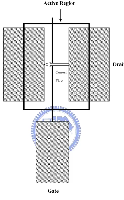
(4) Isolation also addresses the phenomenon know as backside gating or back-gating. The simply device layout is illustrated in Figure 2-6. The source and drain metal
contact the active region and the current is forced to flow between source and drain and under the gate finger. In addition, the shape of the mesa edge is important. The presence of a step can cause difficulties in metal step coverage. If the edge profile is too steep or with undercut, these will be difficult for metallization over this edge. For the discrete device, the mesa isolation was performed by using HF-based solution and etched stop on buffer layer. The ideal profile for mesa isolation is shown in Figure 2-7. The isolation property can be inspected by the Current-Voltage measurement; the measured pattern and results are shown in Figure 2-8 and 2-9, respectively. According to the measurement results, the isolation characteristics and the epitaxy quality are excellent.
2-3 Ohmic Contact
The saturation voltage and the transconductance of the HEMT device are very sensitive to the contact resistance value of the device. The purpose of the ohmic contact on a semiconductor is allowing electrical current flow into or out of the semiconductor. The ohmic contact should have a linear I_V characteristics, be stable over time and temperature. Therefore, an ohmic contact is a low resistance junction providing conduction in both directions. Two general types of ohmic contacts are possible: The first type is the ideal none rectifying barrier, and the second is the
tunneling barrier [1]-[4].
In generally, if simply placing a metal in contact with the wide band-gap III-V semiconductor such as GaAs, it will result in a rectifying contact (a diode) rather than ohmic one [8] [9]. Theoretically, ohmic contacts are formed by joining an n-type semiconductor with work function ψS to a metal with smaller work function ψM,
i.e., ψS >ψM. This situation is shown in Figure 2-10. The Fermi levels are aligned
by the transfer electrons from the metal to the semiconductor. The excess electron charges in the n-type semiconductor exist essentially as a surface charge density which makes the surface of the semiconductor more n-type. If a positive voltage is applied to the metal, there is no barrier for electrons flowing from the semiconductor into the metal. If a positive voltage is applied to the semiconductor, the effective barrier height for the electrons flowing from the metal into the semiconductor will be approximately ψBn=ψn, which is fairly small for a moderately to heavily doped
semiconductor [9].
Figure 2-11a shows the energy band diagram when positive voltage is applied to the metal with respect to the semiconductor. Electrons can easily flow “downhill” from the semiconductor into the metal. Figure 2-11b shoes the case when a positive voltage is applied to the semiconductor with respect to the metal. Electrons can easily flow over the barrier from the metal into the semiconductor [9]. This junction is that
we called an “ohmic contact”.
Real ohmic contacts are fabricated by heavily doped semiconductor. If the doping is sufficiently high, the probability of tunneling through the barrier increases. Figure 2-12 shows a junction in which the metal is in contact with a heavily doped n-type epitaxial layer.
For ohmic metallization, the Au-Ge/Ni/Au system has been widely used as the ohmic contact to PHEMT. The alloyed AuGe ohmic contacts are formed through the alloying reaction of suitable metals with GaAs at temperatures higher than 400℃. As the annealing temperature increases, the AuGe alloy begins to melt and gallium diffuse into the metal. A small amount of arsenic evolves. Germanium atoms diffuses into the GaAs and act as dopants. The heavily Ge-doped GaAs layer formed below the contacts reduces the depletion layer width, resulting in the increase of the electron tunneling probability at the metal/GaAs interface [1]. In this contact system Nickel act as a wetting agent which prevents “balling up" of the metal and forms a conductive NiAs compound. In addition, the use of a top capping layer of gold can improve contact resistance. However, too much gold could getter more gallium than there is germanium available to replace it. It will result in gallium vacancies and cause a high resistance region [1].
optical microscope. The metal will appear splotchy, having dark and light spots when viewed in a microscope. In fact, general experience is that such an appearance is necessary for forming the lowest resistance contacts. A contact that is either “over-alloyed” or “under-alloyed” will not only have a poorer contact resistance, but will also form a different morphology. Examples of these appearances are illustrated in Figure 2-13. From the experience, when there are 50 to 100 black spots in 100μm2, the contact resistance is usually better.
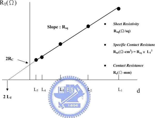
The basic technique used to measure contact resistance of planar ohmic contacts employs a test pattern composed of differently spaced ohmic contact pattern, as shown in Figure 2-14. A plot of the measured resistance as a function of spacing, L, will yield a straight line, as show in Figure 2-15. The slope leads to the sheet resistance with the contact width W independently measured. The intercept at L = 0 is RT = 2 RC giving the contact resistance. The intercept at RT = 0 gives –d = 2LT, which
in turn can be used to calculate the specific contact resistance. The transfer length method gives a complete characterization of the contact by providing the sheet resistance, the contact resistance, and the specific contact resistance. The optimization contact resistance is plotted as a function of alloy temperature as present in Figure 2-16.
2-4 Gate formation
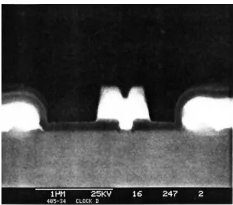
In addition to the short gate length, a small gate resistance is essential for HEMTs for high gain, low noise, and high power applications. A short gate length is also important for high frequency and high speed HEMT devices. In general, one conventional approach for achieving low gate resistance is the use of a T-shaped or mushroom-shaped gate. In the T-shape structure, the small footprint defines the length and the wide top provides a low resistance. T-shape gates have been fabricated using Deep UV lithography or using multilayer resist technique with e-beam lithography. Figure 2-17 illustrates the process flow of using Deep-UV lithography. The SEM image of a 0.5μm T-shaped gate is shown in Figure 2-18. The process flow of forming 0.15μm T-gate bi-layer PMMA/PMMA-MAA photo-resist and the SEM image of lifted-off metal gate are shown in Figure 2-19 and 2-20, respectively.
The selective wet chemical gate recess etching has been widely used to achieve good current and threshold voltage uniformity for the HEMTs. From the previously reports, many efforts have been made to achieve a high selective etch between GaAs/AlGaAs. The etch Selectivity by using different solutions with various x values of the GaAs/AlxGa1-xAs structures are summarized in Table 2-2. In citric acid system,
the selectivity of 2700, 159, 143, 137 for GaAs over AlxGa1-xAs with x=1, x=0.3,
The wet etching mechanisms generally include both diffusion limited and reaction rate limited process. Wet chemical etching proceeds through chemical reactions that occurred at the surface of the material. The etchant must reach the surface in order that appropriate reactions could occur and the reaction products should be removed from the surface. If the etching is reaction rate limited, then the material dissolution is a function of the chemical reaction rate between the etchant and the semiconductor.
For the reaction rate limited mechanism, etching rate is linearly proportional to the etching time, and is unaffected by stirring or agitation of the liquid etchant. If it is diffusion limited etching, the material dissolution depends on the transport of the active etching components to the material surface and on the removal of the reaction products away from the surface. Therefore, etching rate is proportional to the square root of the etching time, and increases with the agitation of the liquid etchants.
In generally, the etchants will contain oxidizer and the dissolving agent. The hydrogen peroxide is usually used as the oxidizing agent. The citric acid based solution is the dissolving agents in the selective etching solution. Most etchants for GaAs operate by oxidizing the surface first and then dissolve the oxides, thereby removing the reacted oxides. As a results, the lower etch rate was observed for AlxGa1-xAs with increasing x
due to the formation of AlxOy which is difficult to remove by the citric acid.
is recessed to achieve the desired channel current and threshold voltage. In addition, the donor layer of the HEMT is very thin and heavily doped, therefore, the HEMT gate recess is more difficult to control than that of GaAs MESFET. The depth to which the gate is recessed is a critical parameter in FET performance. The method used to control the etch depth is to monitor the source-to-drain current during the etching process. The saturated current is reduced as the slot is etched into slice as shown in Figure 2-21 and the test key of current monitor as shown in Figure 2-22. The slot is etched until the target recess current is reached. This requires alternate steps of etching and current measurement, so it is not possible to monitor current while wet etching is proceeding. The concentration of the etchant should be adjusted to provide an etch rate that is sufficiently slow to allow good control over recess process, and reach the target current value without overshooting. Placing the metallization on the GaAs creates a zero-bias depletion zone in the GaAs and results in a saturated drain current drop after metallization. Therefore, the recess etching process must use a target current than that of the desired device current.
Pseudomorphic HEMTs have demonstrated exceptional power performance at millimeter frequency. The limiting factor of power performance has been the relatively low gate-drain breakdown voltage. The use of an undoped cap has been suggested to alleviate this limitation. However, this can increase both the source and
drain parasitic resistances leading to degraded microwave performance. A common technique used to improve the breakdown voltage while maintaining low source resistance is to use a doped cap and offset the gate toward the source side of a wide recess trench. This process requires two lithography steps, one to define the large area where the doped cap is to be removed, and the other to define the much narrower region for gate recess and metallization, as illustrated in Figure 2-23.
After gate recess process, the wafer was cleaned in the solution of HCL: H2O =
1:10 solution to remove the native oxide and the gate metal Ti/Pt/Au was deposited by e-beam evaporator [1].
2-5 Device Passivation
HEMT devices are sensitive to surface effects in the device channel area. Long term degradation can occur due to oxidation or particulate contamination. Dielectric films are typically used in GaAs process for environmental encapsulation. The dielectric seals the surface, keeping humidity, chemicals, gases, and particles away from the sensitive areas of the device. Device passivation requires a pin-hole free, uniform, and low-loss dielectric film [3].
Silicon nitride (Si3N4) was used for passivation by using plasma-enhanced chemical
thickness is about 100nm and the refraction index is 2.0. Figure 2-25 illustrates the dependence of the refraction index of a PECVD silicon nitride film with SiH4. Then,
passivation via-hole pattern was defined by lithography and reactive ion etching (RIE) was performed to etch the silicon nitride film.
2-6 Plating and Bridge Interconnections
Planting process is the last major step for the front-side process. This process is used to connect electrodes of the device with cross over the lower level metallization. Air has a dielectric constant of one; therefore the parasitic capacitance between the bridge and metallization beneath can be reduced.
Gold Plating are usually used for air bridges due to the fact that it has good electrical conductivity, is easily soldered or welded and is resistant to oxidation. Gold is not only ductile, but also resistant to the attack by most acids. Gold used in the microelectronics is very pure, usually 99.99% or even better [1].
Planting air Bridges are illustrated in Figure 2-26 and are widely used in the GaAs devices and MMICs for interconnections. They are used as interconnect for FETs to cross over a lower level of metallization, or to connect the top plate of a MIM capacitor. Usually, there is only air between the bridge and the wafer beneath; this is why they are called air-bridges.
GaAs RF devices requires low parasitic resistance, therefore benefit from the metal thickness of the plated gold. Overall, air-bridge crossover is less capacitive than the crossover with dielectric layer by a factor of five to twenty typically [1].
The major typical steps of processes are illustrated in Figure 2-27. A layer of resist is spun and patterned for metal pads. The thickness of the first layer of resist determines the spacing between the bridge and material beneath. Hence, this layer of resist is usually rather thick – on the order of 2 to 4 μm. Then thin Ti/Au/Ti metal layers were deposited by evaporator. Next, a second coating of resist is applied and patterned. Then, the top of Ti layer would be removed by wet chemical etching, thus the thin Au metal layer could conduct the planting current through the whole wafer. After Au planting, the top resist, thin metal, and lower resist are removed, leaving the planting air-bridge.
2-7 Back- side process
As shown in Figure 2-28, the back side process of the HEMT consists of four major processing steps. The final steps in HEMT fabrication are wafer thinning and via-hole formation. The substrate is thinned from the backside to impose thermal impedance and to make it easy for chip separation. A final substrate thickness of 4 mils is typically used for microwave low noise HEMTs and MMICs. For power application, a
substrate thickness of 2 mils has been adopted for lower thermal impedance [3].
The via-holes provide low-inductance source grounding which is critically important for high frequency power HEMTs. Via-holes can be formed with a wet chemical etch or RIE dry etch. The RIE via-holes process is less sensitive to the uniformity of the final substrate thickness and also provides smaller vias with controlled etch profile [1] [3]. For a multi-fingers power device, small RIE via holes can be placed directly under each source finger or pad for better thermal inductance.
After the via hole formation, the backside of the wafer is metallized as shown in Figure 2-29. The chips are then separated through a wafer sawing or a scribe-and-break.
Al mole fraction of AlxGa1-xAs Volume ratio of 50% citric acid/H2O2 Selectivity 1.0 0.45 0.3 0.3 0.3 0.3 0.28 0.28 0.23 0.2 0.2 0.15 1.5:1 4:1 10:1 5:1 3:1 1.5:1 1:2 4:1 1.5:1 3:1 1.5:1 3:1 2700 260 95 116 155 159 200 80 143 43 137 23
Table 2-1 Selectivity of using different solutions with various x values of the GaAs/AlxGa1-xAs structures.
Figure 2-1 Schematic of the cross section of the conventional HEMT [3].
Figure 2-3 Lattice constant versus band-gap for III-V material[3]
Figure 2-5 The comparison of the structure and the band diagram of the conventional HEMT and Pseudomorphic HEMT [3].
Figure 2-6 Schematic of the device layout Gate Drain Source Active Region Current Flow
Figure 2-7 The ideal mesa edge profiles produced on (100) GaAs surfaces by using HF solution.
Figure 2-9 Device isolation I-V characteristic. 0 10 20 30 40 50 0 50 100 150 200
Current (10
-6A)
V (V)
Figure 2-10 Band diagram for an idealized ohmic contact for a metal –N type-semiconductor junction (a) before contact and (b) after contact [9].
Figure 2-11 Ideal energy-band diagram of a metal- n type semiconductor ohmic contact. (a) with a positive voltage applied to the metal and (b) with a positive voltage applied to the semiconductor [9].
Figure 2-12 Energy band diagram of a heavily doped n-semiconductor to metal junction[9].
3μm 5μm 10μm 20μm 36μm L1 L2 L3 L4 L5
Active Region Contact Pad
W
Figure 2-14 Ohmic contacts are separated by increasing distances.
Figure 2-13 Alloyed AuGe/Ni/Au contacts, showing typical patterns if (a) under-alloyed; (b) alloyed correctly; (c) over-alloyed
Slope : Rsq
RT(Ω)
d
L1 L2 L3 L4 L5 2RC 2 LT z Sheet Resistivity Rsq(Ω/sq)z Specific Contact Resistance
Rsc(Ω-cm2) = Rsq × LT2
z Contact Resistance
Rc(Ω-mm)
1 .0 0 E -0 7 1 .0 0 E -0 6 1 .0 0 E -0 5 1 .0 0 E -0 4 1 .0 0 E -0 3 1 .0 0 E -0 2 2 9 0 3 0 0 3 1 0 3 2 0 3 3 0 3 4 0 3 5 0 3 6 0 3 7 0 Te m p e ra tu re (D e g re e C ) Cont ac t R es is tanc e (O hm -c m *2)
Figure 2-16 Plot of the contact resistance as a function of alloy temperature.
.
Spin 0.2um PMMA ( Bake at 180℃)
PMMA
Spin 0.6um PMMA-MAA (bake at 180℃)
PMMA -MAA
PMMA 495K
Exposure and Develop in developer MIBK:IPA – 180 sec
PMMA
PMMA PMMA-MAA
Spin 0.2um PMMA 495K (bake at 180degC)
PMMA
Spin 0.2um PMMA ( Bake at 180℃)
Spin 0.2um PMMA ( Bake at 180℃)
Gate Metalize, (Tape Lift and Solvent Clean not shown)
PMMA
PMMA PMMA-MAA
Figure 2-18 SEM image of the 0.5μm tri-layer T-shaped gate using D-UV aligner.
Figure 2-19 Process flow of the bi-layer T-shaped gate.
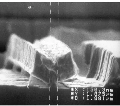
Figure 2-20 SEM image of the 0.15μm T-shaped gate using E-beam writer.
Figure 2-22 The test key for the current monitor after recess etch
Figure 2-21 Saturation current before gate recess, after gate recess, and after gate metallization [1].
Refraction Index
SiH4 (sccm)
Figure 2-25 Dependence of the refracting index of a PECVD silicon nitride film on the of SiH4 flow rate.
First Resist Layer Contact Area
Seed Layer for Plating
Second Resist Layer
Plated Bridge
Resist Removed
Substrate Thinning
Via Hole Formation
Via Hole Formation
Chip Dicing
Screening & Testing
Chapter 3
Device Characterizations
3-1 DC characteristics
The DC characteristics also directly related to the high frequency performance, such as gain, noise figure, and power performance. The DC characteristics in this study are listed below.
Drain-to-Source Current (IDS)-The two currents of interest in HEMT are follows:
IDSS = the saturate source drain current (Vgs = 0V)
Imax= the maximum source-drain current (under forward gate bias)
The methods normally used to specify IDSS as the source-drain current at specified
source-drain voltage with Vgs =0, as seen point A on the Figure 3-1. Figure 3-1 shows the conventional current-voltage characteristic of a 0.25μm × 160μm device. Imax is
determined by forward biasing gate and limited by forward breakdown voltage. The preferred method is to specify the forward gate current (per unit gate width) and to define Imax to be the source-drain current at the forward gate current [1].
Knee voltage- This parameter is defined as the voltage source and drain at which current saturation occurs. The definition is illustrated point B on the Figure 3-1: the intersection of lines fitted to the linear and saturated parts of the trace [1]
Pinch-off voltage-This parameter is the gate voltage at which the drain-to-source current is reduced to a given value, usually 1mA/mm or 1%~2% of IDSS. See point C
on the curves in Figure 3-1.
Transconductance (gm)-This parameter is the DC common source conductance;
that is the incremental change in drain current with a given change in gate voltage. The transconductance is defined as:
g
m= ΔI
ds/ΔV
gsFigure 3-2 presents the measured transconductance of a 0.25μm × 160μm device as a function of the gate-source voltage. The transconductance is essentially zero for gate bias levels below the pinch-off voltage. As the gate bias is toward zero, the transconductance increases monotonically. The device transconductance is greatly affected by the device dimensions and the channel material property. Because of the drain current and the transconductance are directly proportional to the gate width. For this reason, comparisons between devices are often made by examining the transconductance per unit gate width [1].
Breakdown voltage-The breakdown characteristics of the gate can be measured in both directions (gate-to-drain and gate-to –source). In general, only one of the two is needed to verify device characteristics. Most often the gate-to-drain breakdown characteristic is used. The breakdown voltage is a function not only of material
parameters (doping level, energy band gap, Schottky barrier height, etc), but also are highly sensitive to surface conditions near the gate region. The breakdown voltage is also dependent on the device geometry, especially the gate-to-source spacing. If the gate is offset toward the source, the breakdown voltage on the drain side will be greater than that on the source side. There are two ways of characterizing the breakdown characteristic: Specifying the gate-to-drain current and measuring the voltage at that point (BVgd), or specifying the voltage and measuring the reverse
current (Igd). In either case, they are failing when either the reverse current exceeds
the specified value or the breakdown voltage is lower than the specified value [10].
3-2 Scattering Parameter
Scattering Parameters, generally referred to as S-parameter, are fundamental to microwave measurement. These parameters completely and uniquely define the small signal gain and input/output emittance properties of any linear two port network [10]. S-parameters are defined analytically by:
b1 = S11a1 + S22a2 b2 = S21a1 + S22a2
where (referring to Figure 3-4): a1 = (Incoming power at port 1)1/2
b1 = (Outgoing power at port 1)1/2
a2 = (Incoming power at port 2)1/2
b2 = (Outgoing power at port 2)1/2
E1,E2 = Electrical stimuli at Port 1, Port 2
zo = Characteristic Impedance = (50 +j0) Ohms
From Figure 3-4 and define linear equations for E2 = 0, then a2 = 0, and:
S11 = 1
1
b
a = input reflection coefficient
S21 = 2
1
b
a = forward transmission coefficient
S12 = 1
2
b
a = reverse reflection coefficient
S22 = 2
2
b
a = output reflection coefficient
|S21|2 = power gain with load and source impedance
With this information, the functional relationships to gain, stability, input and output matching impedance can be readily derived from the S-parameters. Table 3-1 lists the most useful relationships required for device characterization.
Available power gain - It is the ratio of the power available at the output of a network to the power available from the generator. Available gain is a function of the network s-parameters and the source reflection coefficient. It is independent on the load reflection coefficient.
Stability factor (K factor) - A two port network is unconditionally stable (K>1) if there exists no combination of passive load or source impedances which will allow the circuit to oscillate [10].
Maximum available gain - It is the power gain obtained when the input and output ports are simultaneously conjugated matched to source and load impedances, respectively. Implicit in the definition is the assumption that two port device is unconditionally stable. On the other hand, the maximum available gain (MAG) of a device is only defined where K is greater than one. This is because the term under the square-root becomes negative for values of K less than 1. Another way to look at it is that maximum available gain is infinite. Infinite gain means oscillator.
Maximum stable gain - The maximum stable gain (MSG) of a device is defined when maximum available gain is undefined (K<1). It is merely the ratio of S21 /S12 .
Under no circumstances should you try to treat more than this amount of gain from a conditionally stable device. The MSG can be obtained if the transistor is potentially unstable according to the equation:
21 1 12 K
S
MSG
MAG
S
==
=
Unilateral power gain - The power gain of a transistor amplifier when lossless
feedback has been used to neutralize the reverse transfer coefficient (S12) to zero; the input reflection coefficient (S11) has been matched to zero with lossless circuit elements; and the output reflection coefficient has been matched to zero with lossless circuit elements. The unilateral power gain is the highest power gain which can be achieved from the transistor, and the frequency where this gain is zero dB is fmax [10].
3-3 F
tand F
maxTwo parameters often used to characterize devices are Ft and Fmax. These quantities
represent the unity gain intercept point of the short circuit current gain (h21) and
unilateral power gain, respectively. Table 3-2 lists the y and h parameters in terms of S-parameters. The unity short-circuit current gain frequency (Ft) is defined to be a
frequency at which h21 becomes equal to 0 dB. In addition, Ft is also measured by
extrapolating h21 to unity gain with 20dB/decade slope as shown in Figure 3-5.
The maximum frequency of oscillation, fmax, is the frequency at which a curve of unilateral power gain (U) vs. frequency intercepts zero dB gain as shown in Figure 3-5. The unilateral power gain of HEMT transistors decay at a slope of approximately 20dB/decade. If gain is measured at convenient frequencies between 2 and 12 GHz the points will approximately fit a straight line curve when gain in dB is plotted on a
linear vertical scale against frequency plotted on a log scale horizontally [10]. The frequency at which the unilateral power gain extrapolates to 0 dB gain is fmax.
3-4 Noise Figure
Modern wireless receiver needs to deal with very weak signals, but the noise added by the system components tends to obscure those very weak signals. Sensitivity, bit error ratio (BER) and noise figure are system parameters that characterize the ability to process low level signals. Of these parameters, noise figure is not only for characterizing the entire system but also the system components such as the pre-amplifier, mixer, and IF amplifier that make up the system. Noise figure is often the key parameter that differentiates one system from another, one amplifier from another and one transistor from another [10].
The reason for measuring noise properties of the networks is to minimize the problem of noise generated in receiving systems. One approach to overcome noise is to make the weak signal stronger. This can be accomplished by raising the signal power transmitted in the direction of the receiver, or by increasing the amount of power the receiving antenna intercepts, for example, by increasing the aperture of the receiving antenna. Raising antenna gain, which usually means a larger antenna, and raising the transmitter power, are eventually limited by government regulations,
engineering considerations, or economics. The other approach is to minimize the noise generated within receiver components. Noise measurements are keys to assuring that the added noise is minimal. Once noise joins the signals, receiver components can no longer distinguish noise in the signal frequency band from legitimate signal fluctuations. The signal and noise get processed together. Subsequently raising of the signal level with gain, for example, will raise the noise level an equal amount. Figure 3-6 shows a generalized block diagram of a typical noise figure setup used to obtain noise parameters [10].
Today, conventional AlGaAs/InGaAs HEMTs have demonstrated unprecedented noise performance at cryogenic temperatures, good microwave and millimeter-wave noise performance at room temperature at frequencies up to 60 GHz, and very high gate-switching speeds in digital circuits. The minimum noise figure of a HEMT can be expressed as: min
(
) 10log(1
)
g s gs mR
R
F
dB
kfC
g
+
=
+
Where Fmin is the minimum noise figure, k is the Fukui constant, F is frequency, Cgs is
input gate capacitance, and Rg and Rs are the gate and source resistances, respectively.
For superior low-noise performance, the device must have low Fukui constant, high transconductance, and low parasitic gate resistance, source resistance, and capacitance.

![Figure 1-3 The band diagram of the E-PHEMT at three different gate voltages[6].](https://thumb-ap.123doks.com/thumbv2/9libinfo/8395623.178926/33.892.156.769.517.878/figure-band-diagram-e-phemt-different-gate-voltages.webp)
![Figure 2-1 Schematic of the cross section of the conventional HEMT [3].](https://thumb-ap.123doks.com/thumbv2/9libinfo/8395623.178926/50.892.237.642.345.605/figure-schematic-cross-section-conventional-hemt.webp)
![Figure 2-10 Band diagram for an idealized ohmic contact for a metal –N type-semiconductor junction (a) before contact and (b) after contact [9]](https://thumb-ap.123doks.com/thumbv2/9libinfo/8395623.178926/57.892.155.753.167.386/figure-diagram-idealized-contact-semiconductor-junction-contact-contact.webp)
![Figure 2-21 Saturation current before gate recess, after gate recess, and after gate metallization [1]](https://thumb-ap.123doks.com/thumbv2/9libinfo/8395623.178926/65.892.312.552.554.949/figure-saturation-current-gate-recess-gate-recess-metallization.webp)