國立交通大學
電機學院微電子奈米科技產業研發碩士班
碩 士 論 文
氮氣和熱處理對氧化鉿薄膜的電阻式記憶體電性之效應
Effect of nitrogen and thermal treatment on
resistance random
access memory (RRAM) for HfO
xfilm
研 究 生:吳天佑
指導教授:汪大暉 教授
氮氣和熱處理對氧化鉿薄膜的電阻式記憶
體電性之效應
Effect of nitrogen and thermal treatment on resistance
random access memory (RRAM) for HfO
xfilm
研 究 生:吳天佑 Student:Tien-Yu Wu
指導教授:汪大暉教授 Advisor:Dr. Tahui Wang
國 立 交 通 大 學
電機學院微電子奈米科技產業研發碩士班
碩 士 論 文
A Thesis
Submitted to College of Electrical and Computer Engineering National Chiao Tung University
in partial Fulfillment of the Requirements for the Degree of
Master In
Industrial Technology R & D Master Program on Microelectronics and Nano Sciences
August 2009
Hsinchu, Taiwan, Republic of China
氮氣和熱處理對氧化鉿薄膜的電阻式記憶
體電性之效應
學生:吳天佑 指導教授:汪大暉
國立交通大學電機學院產業研發碩士班
摘 要
近年來,非揮發記憶體的研究越來越多,其中以阻態式記憶體最受關注。它 有簡單結構、低消耗功率、操作速度快、低操作電壓、保存時間長、高耐用度、 非破壞性讀取和小的尺寸。因此阻態式記憶體被提議是下一代非揮發性記憶體的 候選。 在這篇論文中,氧化鉿阻態式記憶體提供一個高密度和低功耗應用與製程整 合。首先,我們先介紹雙阻態操作的電壓電流特性。我們使用濺鍍方法,上電極 分別是鈀和鈀/鋁分別作不同的處理並探討這些處理對電性效應的探討報告。最 後,我們將歸納出元件的電流傳導機制,探討不同處理對元件的影響,我們選擇 低電壓的操作作為往後的發展元件。Effect of nitrogen and thermal treatment on resistance
random access memory (RRAM) for HfO
xfilm
student:Tien-Yu Wu Advisors: Dr. Tahui Wang
Industrial Technology R & D Master Program of
Electrical and Computer Engineering College
National Chiao Tung University
ABSTRACT
In recent years, nonvolatile memory research of person more and more, among them in order to resistive random access memory (RRAM) have attracted a large attention, including simple structure, low power consumption, high operation speed, low operation voltage, long retention time, high endurance, non-destruvtive readout, and small cell size. Accordingly, RRAM has been proposed to be one candidate of next generation nonvolatile memory.
In this thesis, the HfO2 resistive switching device offers a promising potential for
high density and low power memory application with the ease of processing integration. First, we would introduce fundamental Current-Voltage characters of the bistable resistive switching behavior. The Pd and Pd/Al was doped top electrical with different treatment by sputtering method, and discussion treatment effect. Finally, we would decline the conduction mechanism of the device and discuss the influence of treatment. We would choose is operation of low-voltage as development component later.
致 謝
首先感謝我的指導教授張國明老師及汪大暉老師,在這兩年的碩
班生涯的指導,使我在研究上可以順利的完成。張國明老師開明的指
導方式,不但讓我學到做研究該有的科學思考,也習得待人處事的道
理。而老師也不忘在會議時,不時的提醒我們努力研究,回饋社會。
再來要感謝曾文賢學長對我初期實驗的方向作了指引,使我有一個明
確的方向進行實驗,感謝實驗室菘宏學長實驗機台的教導與分析儀器
的協助,可以讓我在實驗分析上順利的進行,以便我後續的實驗進
行,感謝口試委員在口試時的指導,感謝這一路走來協助我的人,若
不是你們的幫忙,本論文無法如此順利的完成。
最後要感謝我的父母吳耀煌先生與鐘玉花女士與我的兄姐及親
友,全力支持我念研究所,無論是在精神上或是物質上的協助及鼓
舞,讓我無後顧之憂全力專心在課業上,我才能順利完成學業,謝謝
你們!
Contents
Abstract (in Chinese)...i
Abstract (in English)...ii
Acknowledgement...iii
Contents ...iv
Table Captions ...vi
Figure Captions ...vi
CHAPTER 1 Introduction………..1
1.1 Introduction to Nonvolatile Memory (NVM) ……….…... 1
1.1.1 Introduction to FeRAM (Ferroelectric Random Access
Memory)………..………...1
1.1.2 Introduction to MRAM (Magnetic Random Access
Memory)……….………..2
1.1.3 Introduction to PCRAM (Phase Change Random Access
Memory)……….………..5
1.1.4 Introduction to Resistive Random Access Memory
(RRAM)……….……….……..5
1.2 Mechanism of transition metal oxide (TMO) RRAM….……...…….8
1.2.1 Filamentary model (TMO).………...8
1.2.2 Schottky barrier and space-charged limited conduction
(SCLC)……….9
1.2.3 Frenkel-Poole emission………9
CHAPTER 2 Experiment details……...………...…………....17
2.1 Experiment procedure……….17
2.1.1 Process flow………...17
2.1.2 Top electrode deposition ………..…..………...17
2.1.3 Thermal treatments ……….…………18
2.2 Property analysis……….……..………….18
2.2.1 Film thickness and HfO
xvalence states………18
2.2.2 X-Ray Diffraction (XRD)………..….………..18
2.2.3 Scanning Electron Microscope (SEM)……….………19
2.2.4 Atomic force microscope (AFM) ……..………..19
2.2.5 X-ray photoelectron spectroscopy (XPS)……….19
CHAPTER 3 Results and Discussion………..……23
3.1 Structural analysis………..23
3.1.1 Film thickness and composition….………..23
3.1.2 Crystalline structure……….24
3.2 Pd top electrodes Electrical property……….24
3.3 Pd/Al top electrodes Electrical property………27
3.4 Fitting leakage current property……….30
Chapter 4 Conclusions………..60
TABLE CAPTIONS
Table 1-1 Comparison of the performance of emerging memories……….16
Table 2- 1 Summary of Pd deposition parameters………...22
Table 2- 2 Summary of Pd / Al deposition parameters………22
Table 3-1 comparison Pd/HfOx/TiN sample different treatment negative switch on..58
Table 3-2 comparison Pd/HfOx/TiN sample different treatment positive switch on...58
Table 3-3 comparison Pd/Al/HfOx/TiN sample different treatment negative switch on……….…….…59
Table 3-4 comparison Pd/Al/HfOx/TiN sample different treatment positive switch on………..…59
FIGURE CAPTIONS
Fig. 1- 1 Illustration of ABO3 pervoskite unit cell………..10Fig. 1- 2 Hysteresis loop of a ferroelectric material………10
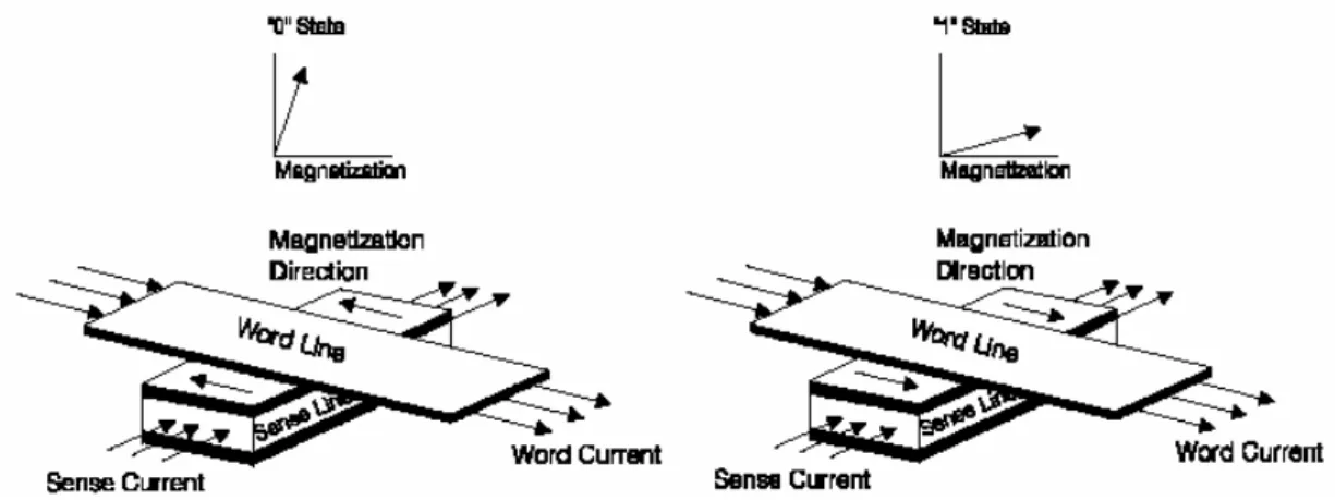
Fig. 1- 3 Illustration of a AMR MRAM cell showing orthogonal word line and sense line for programming……….11
Fig. 1- 4 Illustration of GMR spins valve mechanism……….11
Fig. 1-5 Illustration of a magnetoresistive tunnel junction (MJT)………...11
Fig. 1-6 Illustration of a data storage region in the PCRAM cell………12
Fig. 1-7 (a) Schematic temperature-time relationship during programming in a phase change rewriteable memory device. Tm and Tx are the amorphization and crystallization temperature, respectively. (b) Illustrations of electrical pulse-structure and structure-resistance relationship……….…13
Fig. 1- 8 RRAM cross sectional structure………14
Fig. 1- 9 Typical resistive switching I-V curves………..14
Fig. 10(a) The material between electrodes is gradually charged to small domains (b) toward filament (c) formed with tunneling among adjacent domains and more domains near electrodes (d) (e)………...15
Fig.10(b) Subsequent action of dis-rupture (i.e.” reset”) or re-connect ( i.e.” set”) are similar to “fuse blown” or re-connect of those small domains…………....15
Fig.2-1 The cross section of the Pd/HfOx/TiN device………..21
Fig.2-2 The cross section of the Pd/Al/HfOx/TiN device………....21
Fig 3-1 SEM cross-sectional structure of as deposited HfOx film………...33
Fig 3-2 AFM step height of HfOx/TiN film……….33
Fig 3-3 AFM image of as deposited HfOx film (a) 2d image (b) rms image………...34
Fig 3-5 XPS cross-sectional structure of as deposited HfOx film………35
Fig 3-6 X-ray photoelectron spectra of the Hf 4f region of as deposited HfOx films in surface layer ………36
Fig 3-7 X-ray photoelectron spectra of the Hf 4f region of as deposited HfOx films in interface region………36
Fig 3-8 X-ray diffraction patterns of as-deposited HfOx films………37
Fig 3-9 X-ray diffraction patterns of as-deposited HfOx films and RTA process……37
Fig 3-10 I-V curve of the Pd/HfOx/TiN device………38
Fig 3-11 switch cycle vs. voltage of Pd/HfOx/TiN device ………..38
Fig 3-12 I-V curve of the Pd/HfOx/TiN device after RTA 400℃ for 30s………39
Fig 3-13 I-V curve of the Pd/HfOx/TiN device after RTA 400℃ for 30s for positive switch on negative switch off……….39
Fig 3-14 I-V curve of the Pd/HfOx/TiN device after RTA 400℃ for 1min…………..40
Fig 3-15 I-V curve of the Pd/HfOx/TiN device after RTA 400℃ 1min for positive switch on negative switch off……….40
Fig 3-16 comparison thermal treatment of the Pd/HfOx/TiN device………...41
Fig 3-17 comparison sample of thermal treatment as Pd initial forming……….41
Fig 3-18 comparison sample of thermal treatment at various RTA times…………...42
Fig 3-19 I-V curve as N2 0.5sccm 20s before deposition Pd layer………..42
Fig 3-20 I-V curve as N2 12sccm 20s before deposition Pd layer………...43
Fig 3-21 comparison nitrogen different flow with deposition Pd initial forming……43
Fig 3-22 comparison sample as N2 0.5sccm 20s of thermal treatment at various RTA times.……….….44
Fig 3-23 comparison sample as N2 12 sccm 20s of thermal treatment at various RTA times………....……….…….…44
Fig 3-24 comparison Al layer of thickness………..……45
Fig 3-25 I-V curve of the Pd/Al/HfOx/TiN device for positive switch on negative switch off………..…...45
Fig 3-26 I-V curve of the Pd/Al/HfOx/TiN device as different thermal treatment time ……….….…….46
Fig 3-27 I-V curve of the Pd/Al/HfOx/TiN device……….….……46
Fig 3-28 switch cycle vs. voltage of Pd/Al/HfOx/TiN device……….……47
Fig 3-29 Retention properties of RLow and RHigh at room temp……….…..47
Fig 3-30 comparison nitrogen flow 0.5sccm different time at deposition 35Å Al.…48 Fig 3-31 comparison nitrogen different flow with deposition 35Å Al………….…..48
Fig 3-32 I-V curve of the Pd/AlN/HfOx/TiN device ………..……49
Fig 3-33 I-V curve as N2 6sccm 20s of the Pd/Al/HfOx/TiN device ………….……49
Fig 3-35 comparison nitrogen different flow 20s with deposition 35Å Al………..…50 Fig 3-36 comparison nitrogen different flow with deposition 35Å Al RTA 30s….…51 Fig 3-37 comparison nitrogen different flow with deposition 35Å Al RTA 1min…..51 Fig 3-38 comparison Al 35 RTA resistance state……….……52 Fig 3-39 I-V curve of the Pd/Al/HfOx/TiN device as N 12sccm 20s after RTA 400℃
for 1min……….…….52 Fig 3-40 Retention properties of RLow and RHigh at room temp………53
Fig 3-41 the current fitting of H-state as Pd/HfOx/TiN device as different nitrogen flow I-V curve………..53 Fig 3-42 the current fitting of L-state as Pd/HfOx/TiN device as different nitrogen
flow I-V curve………..………….……….54 Fig 3-43 the current fitting of H-state as Pd/HfOx/TiN device as different thermal
treatment time I-V curve………...54 Fig 3-44 the current fitting of L-state as Pd/HfOx/TiN device as different thermal
treatment I-V curve………55 Fig 3-45 the current fitting of H-state as Pd/Al/HfOx/TiN device as different
nitrogen flow I-V curve……….55 Fig 3-46 the current fitting of L-state as Pd/HfOx/TiN device as different nitrogen
flow I-V curve………...56 Fig 3-47 the current fitting of H-state as Pd/Al/HfOx/TiN device as different
thermal treatment I-V curve……….56 Fig 3-48 the current fitting of L-state as Pd/Al/HfOx/TiN device as different
Chapter 1 Introduction
1.1 Introduction to Nonvolatile Memory (NVM)
In more recent years, nonvolatile memory ( NVM ) have been widely used for Mobile phone, digital camera, and MP3 player. The NVM has been widely investigated since Kahng and Sze introduced that floating gate device. [1] With the increasing usage of NVM requirements for cell size have become more critical. A perfect NVM should have the superior properties, including simple structure, low power consumption, high operation speed, low operation voltage, long retention time, high endurance, non-destruvtive readout, and small cell size [2]. Several next-generation memory technologies have been studied, including FeRAM (Ferroelectric Random Access Memory), MRAM (Magnetic Random Access Memory), PCRAM (Phase Change Random Access Memory), and RRAM (Resistive Random Access Memory) and so on. The basic principles of these emerging memories are shown below.
The emerging memories described above are competing technologies that could replace DRAM, SRAM, EEPROM and Flash. A comparison of these emerging memories is shown in table 1-1.
1.1.1 Introduction to FeRAM (Ferroelectric Random Access Memory)
The ferroelectricity is the ability of a material to retain an electronic polarization in the absence of an applied voltage [3]. This spontaneous polarization results from the alignment of internal dipoles within the crystal units of the ferroelectric material and it can reoriented by the external electric field. Many of ferroelectric materials have pervoskite-type structure which can be expressed mostly ABO3 in formula. The
and oxygen occupy the corner site, body-centered site, and face-centered site, respectively.
Under the influence of an applied voltage, the crystals begin to polarize in the direction of the applied field, i.e. the mobile atoms (B atom) move within the crystals if they are not already in the appropriate positions corresponding to the applied field. The orientation of spontaneous polarization will approach its steady state, which is denoted by a polarization-electric field (P-E) hysteresis loop as shown in Fig. 1-2.
There are two net stable states for the ferroelectric material as the applied voltage is switched. These are defined as “up” and “down” or electrically as “1” and “0” which can be employed as memory application.
1.1.2 Introduction to MRAM (Magnetic Random Access Memory)
Development on magnetic memories has been going on for many years. Magnetic core memories were used in early mainframe computers. It is similar to today’s MRAM in using a matrix of current carrying wires to program magnetic elements [4]. The sensing schemes of them are different; however, the operation of MRAM is much simpler.
MRAM uses an effect called magneto-resistance (MR) which is a change in the electrical resistivity of a material is relation to the orientation of magnetic polarization. Several different types of magneto-resistance have been considered for data storage in different variations of MRAM. The classification of include: Anisotropic Magneto-Resistance (AMR), Giant Magneto-Resistance (GMR), and Tunneling Magneto-Resistance (TMR).
(i) Anisotropic Magneto-Resistance MRAM:
An AMR MRAM cell is a sandwiched structure made of two magnetic Permalloy (NiFeCo) layers separated by TaN interlayer. The data storage media is the change in electrical resistivity of magnetic material as the direction of magnetization is rotated with respect to the direction of current flow from parallel to perpendicular as show in Fig. 1-3.
The percentage change in resistivity is called the magneto-resistive (MR) value. The typical available MR for the two memory state for AMR MRAM is about 0.5~2% of the total MR value [5-6].
(ii) Giant Magneto-Resistance MRAM:
The origin of the GMR effect is the spin-dependent scattering of the conduction carriers within the magnetic layers or at their boundaries which causes variations in the resistance. Moreover, two implementations of the GMR effect have been demonstrated as MRAMs, the spin valve and the pseudo-spin valve [7-8]. Both spin valve technologies use a tri-layer structure consisting of a soft magnetic layer and a hard magnetic layer which are spaced by a thin layer of a non-magnetic metal as shown in Fig. 1-4.
The resistance variation is due to the fact that a single-domain magnetic material will scatter electrons with an “up” and “down” spin differently depending on the direction of magnetization. As the top and bottom magnetic layers in a GMR structure have anti-parallel alignment, the resistance is high because the “up” electrons that are not scattered by one of two magnetic layers will be scattered by the other, thus creating high resistance to the flow of electrons through the GMR structure. In contrast, as the top and bottom magnetic layers in a GMR structure have parallel alignment, the “up” electrons do not scatter very much regardless of which layers they
pass through, resulting in a low resistance to the flow of electrons through the GMR structure. The typical available MR for the two memory state for GMR MRAM is in the range of 6~50% of the total MR value [10-11].
(iii) Tunneling Magneto-Resistance MRAM:
In a TMR MRAM device, two magnetic layers separated by a thin insulating barrier with a few tenths of a nanometer thick as shown in Fig. 1-5.
Under the influence of a small electric bias, current can tunnel through the barrier. The transport of electron across the barrier depends on magnetic orientation of both magnetic layers. The mechanism is “spin polarized tunneling” whose probability depends on the relative orientation of the magnetization vectors in the two magnetic electrodes [13]. The probability of current passing is higher as the magnetic orientations are parallel [14]. In the parallel configuration, there is an optimized match between the number of occupied energy states in one electrode and the number of available states in the other electrode which enhances the tunneling current. In contrast, as they are in an anti-parallel configuration, the tunneling is between majority states in one electrode and minority states in the other. This diminishes the tunneling current.
The difference in the resistance can be 40% or more at room temperature between the parallel and anti-parallel alignment. The conductance, which is the inverse of the resistance, of the MTJ varies as the cosine of the angle between the magnetic moments of the two ferromagnetic layers and the highest conductance can be obtained as the magnetic moments are parallel [14]. Moreover, it should be noted that the process uniformity is critical for the very thin insulating barrier in the MTJ which is commonly made of Al2O3. If the aluminum is over-oxidized or
1.1.3 Introduction to PCRAM (Phase Change Random Access Memory)
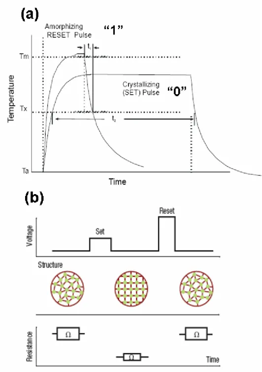
Glassy phase is formed by rapidly super cooling a liquid below its melting point to a temperature at which the atomic motion necessary for crystallization cannot rapidly occur. Chalcogenide alloys such as GeSe, AsS, GeAsTe, AlGe, AsTe, are the materials containing one or more elements from Group VI of the periodic table and they are typically good glass-formers. According to this characteristic, the memory switching in chalcogenide alloys can be operated by a thermal process which involves a reversible phase transformation from an amorphous to a crystal state under the influence of an applied energy source [15]. The schematic structure of a data storage region in the PCRAM cell is shown in Fig. 1-6.
A short pulse of energy was used melt the material, which was then allowed to cool quickly enough to “freeze in” the glassy, structurally disordered state. To reverse the process, lower amplitude, long duration pulse was used to heat a previously vitrified region of the alloy to the temperature below the melting point, at which crystallization could occur rapidly, as shown in Fig. 1-7.
1.1.4 Introduction to Resistive Random Access Memory (RRAM)
RRAM is made of a transistor and a switchable dielectric resistor (Fig. 1-8). On the basis of I–V characteristics, the switching behaviors can be classified into two
types: unipolar (nonpolar) and bipolar, for which typical I–V curves are shown in Fig.
1-9. In unipolar resistive switching, the switching direction depends on the amplitude
of the applied voltage but not on the polarity. An as-prepared memory cell is in a
highly resistive state and is put into a low-resistance state (LRS) by applying a high
voltage stress. This is called the ‘forming processes’. After the forming process, the
cell in a LRS is switched to a high-resistance state (HRS) by applying a threshold
by applying a threshold voltage that is larger than the reset voltage. In the set process,
the current is limited by the current compliance of the control system or, more
practically, by adding a series resistor. This type of switching behavior has been
observed in many highly insulating oxides, such as binary metal oxides. Bipolar
resistive switching shows directional resistive switching depending on the polarity of
the applied voltage (Fig. 1-9). This type of resistive switching behavior occurs with
many semiconducting oxides, such as complex perovskite oxides, and will be
discussed in detail in this review.
RRAM shows superior advantages such as simple structure, low power operation, low power consumption, long retention time, small cell size, fast switching speed and easy compatible with the standard CMOS technology.
Many candidate materials includes binary oxide such as ZrO2 [16]as well as
perovskite-type oxide such as doped-SrZrO3 (SZO) [2, 17] or multi oxide
Pr1-xCaxMnO3 (PCMO) [18, 19] has been proposed, but mechanism of the switching
behavior does not really clear. Although various models for resistive switching have been suggested, e.g., alternation of Schottky barrier, [20]filamentary conduction, [21, 22, 23]and trap-controlled space-charge-limited current, [24]the underlying physical mechanism of resistive switching and the charge transportations in ReRAM is still not yet understood. Electrode effect showed the different switching behavior is needed to be investigated to further understand the switching mechanism. [25] Proposed that resistance switching behaviors of NiO/Pt device was dominated by the work function (WF) of the top metal. When the metal/NiO interface formed ohmic contact, such as Pt/NiO/Pt and Au/NiO/Pt, voltage drops at the interface are omitted and effective electric field inside the NiO film is high enough to induce resistance switching. For Ti/NiO/Pt structure, well-defined Schottky contact at the Ti/NiO interface leading to the effective electric field inside the NiO film is not enough to induce resistance
switching. Lin et al. [26]discussed the effect of top electrode material on resistive switching properties of ZrO2 film. Metal Al, Pt as top electrode shows unipolar
switching with large dispersion of Ron, Roff, Von, and Voff, while metal Ti as top
electrode shows bipolar switching with stable switching behavior. Lee et al. [27] proposed that effect of metal electrodes to NiO RRAM device is correlated to the free energy of oxide formation between electrode and Ni. It seems that top electrode plays an important role to the performance of RRAM device, whether what kind of the transition metal oxide (TMO). HfOx film with Pt, Au and Ru metal as top electrode
respectively has been reported having resistive switching properties [28, 29, 30], but not much mention to the effect of top electrode to the HfOx RRAM device. We observed the electrical characteristics of HfOx/TiN capacitor structure with metal Pd,
Al / Pd, Ti / Pd and TiN as top electrode respectively. Generally, the electrical characteristics changed in an abrupt way by bipolar switching during low resistance state (LRS) to high resistance state (HRS). Mechanism of the switching behavior was proposed here to elucidate the phenomena. Top metal electrode alters not only the type of the switching properties, but also influences the operation dispersion and resistance ratio. Effect of top electrode is crucial to the performance of HfOx RRAM
device.
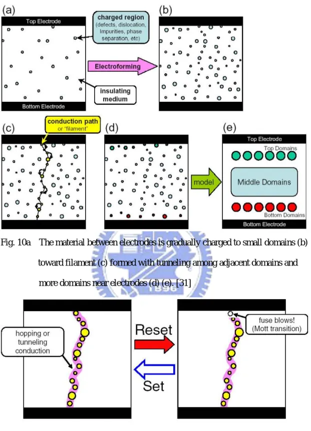
The resistive switching is typically molded as the formation and dis-rupture of conductive filaments based on various physical mechanisms. The 1st mechanism for the filament formation is related to domains (Fig. 1-10) gradually charged up and electron tunneling [31] occurrence eventually among nearby domains. This is adequate to those resistors with “inert” electrodes and insulator based on carrier trapping/de-trapping. The 2nd mechanism [32] is related to metal ions accumulated along grain boundaries and the set/reset of the filament occurred locally near the anodic electrode. This mechanism leads to variations of interface Schottky-like barrier
and is suitable for metal oxide resistive switching with inert electrodes. The 3rd mechanism is based on the movement of O-vacancies and ions [33]. The reset is related to the depletion of electrons in O-vacancies, and the set is due to the recovery of the depleted O-vacancies with non-lattice oxygen ions. The 4rd mechanism is related to the interaction of the resistive switching material with active electrodes.
1.2 Mechanism of transition metal oxide (TMO) RRAM
The binary oxide MIM memory devices were discovered decades ago. This device had not been a serious contender for large scale memory array application. After the publication of “Electric-pulse-induced reversible (EPIR) resistance non-volatile memory” by Liu et al in 2000 [34] the resistance-based MIM memory devices have attracted considerable interest. The ratio of the resistance at the high resistance state to the resistance at the low resistance state of an EPIR resistor can be larger than four orders of magnitude. Liu et al concluded that it is a generic property of oxide in the presence of intrinsic defects, in relation to impurities having different oxidation states and vacancies which can form a series of states at various levels within the energy gap [35].
1.2.1 Filamentary model (TMO)
Cyclic repetitive resistance switching was discovered in crystalline NiO thin films by Gibbons and Beadle [36]. They have ascribed the phenomenon to the repeated formation and rupture of a metallic filament. Hickmott [37] suggested that the filament was composed of immobile neutral impurities in the insulator with ionization energies close to the half of band gap while Simmons suggested the filament was made of injected metal ions from the anode into the insulator [38].
1.2.2
Schottky barrier and space-charged limited conduction (SCLC)
In contrast to a filamentary model, Austin suggested that switching might be caused by the trapping of charge near electrodes and tunneling through the Schottky barrier [39]. It is natural to assume that the Pt/TiO2 junction has a Schottky
characteristic due to the high work function of Pt and the n-type nature of TiO2. An
excessive electron injection at low interfacial barrier results in negative charge accumulation in the TiO2 film which leads to space charge limited conduction (SCLC).
The SCLC might suppress the switching due to the effective reduction of the electric field at the interface [40].
1.2.3 Frenkel-Poole emission
Electrons can move (slowly) through an insulator by the following method. The electrons are generally trapped in localized states (loosely speaking, they are "stuck" to a single atom, and not free to move around the crystal). Occasionally, random thermal fluctuations will give that electron enough energy to get out of its localized state, and move to the conduction band. Once there, the electron can move through the crystal, for a brief amount of time, before relaxing into another localized state (in other words, "sticking" to a different atom). The Poole–Frenkel effect describes how, in a large electric field, the electron doesn't need as much thermal energy to get into the conduction band (since part of this energy comes from being pulled by the electric field), so it does not need as large a thermal fluctuation and will be able to move more frequently.
Taking everything into account (both the frequency with which electrons get excited into the conduction band, and their motion once they're there), the standard
quantitative expression for the Poole–Frenkel effect is: ) ( exp( T K qE q E J B B πε φ − − ∝
Fig. 1- 1 Illustration of ABO3 pervoskite unit cell
Fig. 1- 3 Illustration of a AMR MRAM cell showing orthogonal word line and sense line for programming
Fig. 1- 4 Illustration of GMR spins valve mechanism [9].
Fig. 1-7 (a) Schematic temperature-time relationship during programming in a phase-change rewriteable memory device. Tm and Tx are the amorphization and crystallization temperature, respectively. (b) Illustrations of electrical pulse-structure and structure-resistance relationship.
Fig. 1- 8 RRAM cross sectional structure
Fig. 10a The material between electrodes is gradually charged to small domains (b) toward filament (c) formed with tunneling among adjacent domains and
more domains near electrodes (d) (e). [31]
Fig.10b Subsequent action of dis-rupture (i.e.” reset”) or re-connect(i.e.” set”) are similar to “fuse blown” or re-connect of those small domains. [31]
Table 1-1 Comparison of the performance of emerging memories [40] NOR Flash (1T) FeRAM (1T1C) MRAM (1T1R) PCM (1T1R) RRAM (1T1R) Cell Area 4F2 20F2 20F2 6F2 4F2 Read Time 70-90 ns 45 ns 20 ns 60 ns <50 ns W/E Time >1 ms <20 ns <0.5 ns <60 ns <50 ns Retention Time >10 y >10 y >10 y >10 y >10 y Write Cycles >105 1014 >3x10¹⁶ 108 >105 Write Voltage(V) 12 0.9-3.3 1.5 3 <3 Read Voltage(V) 4-5 0.9-3.3 1.5 3 0.7
Chapter 2 Experiment Detail
2.1 Experiment procedure
2.1.1 Process flow
The HfOx/ TiN memory devices were fabricated on an 8 in. Si wafer. A thickness
of 30 nm HfOx thin film with non-stoichiometry was deposited on the TiN layer by
atomic layer deposition at temperature of 300℃. Hafnium tetrachloride (HfCl4) and
water (H2O) with the composition ratio = 5:2 were used as reactants in the ALD
process. In order to verify the resistance switching behavior related to the crystalline structures of HfOx, the HfOx films were examined by using X-Ray Diffraction System
(XRD) before covering the top electrodes. I -V characteristics of the HfOx films were
measured by computer-interfaced HP4156C (Sweep mode). The X-ray photoelectron spectroscopy (XPS) was also employed to identify the composition of HfOx films.
The film microstructures were investigated by Scanning Electron Microscope System
(SEM) and Atomic force microscope (AFM).
The electrical characteristics of the HfOx/TiN RRAM device were performed on an Agilent 4156C semiconductor parameter analyzer. Bias voltage was applied on the top electrode with the TiN bottom electrode grounded. All the measurements were performed at room temperature.
2.1.2 Top electrode deposition
The 30nm Pd and 3.5nm Al / 30nm Pd top electrode were deposited on the HfOx
film by dc Sputtering System with a shadow mask at room temperature, the structure is shown in Fig. 2-1, Fig 2-2 . We set the dc power 80W Pd、40W Al and the chamber pressure in 7.6 mtorr. The open nitrogen flow is 0.5、1、4、6、12 sccm 20 second before depositing Al.
2.1.3 Thermal treatments
After top electrode deposition, some samples were processed with RTA (rapid thermal annealing in argon atmosphere) system at 400 for 30sec and 1min, ℃ respectively. Table 2-1 shows the summary of Pd deposition parameters. Table 2- 2 shows the summary of Al/Pd deposition parameters.
2.2 Property analysis
2.2.1 Film thickness and HfO
xvalence states
The Scanning Electron Microscope System (SEM)、X-Ray Diffraction System (XRD)、Atomic force microscope (AFM) and X-ray photoelectron spectroscopy (XPS) were used to obtain the micro-structure and the crystallization of the films. AFM and SEM analysis could help us to understand the surface roughness and thickness of HfOx film. XRD analysis helped us to confirm the orientation of the film. XPS
analysis helped us to examined chemical bonding energy of the film.
2.2.2 X-Ray Diffraction (XRD)
Generally, thin films are classified according to its crystallization. There are three types of crystallization, including amorphous, polycrystalline, and single. X-Ray Diffraction analysis is used to investigate the crystal structure and orientation of our sample. Furthermore, we could identify the crystallization dependence of on the samples for heat treatment. In our experiment, the thin films were grown between amorphous type and poly type. Follow Scherrer’s formula, we could calculate the average grain size from XRD illustration:
θ λ cos 9 . 0 × × = B D
the full width at half maximum (FWHM) of the XRD peak and θ is the diffraction angle. In this analysis, X-ray is made with 0.02 degree beam divergence and operation configuration at 30KV, 20mA.
2.2.3 Scanning Electron Microscope (SEM)
Comprehensively, the surface morphology issue is also a quite important character compared with the character of bulk for the thin films. We could observe the surface micro-morphology and cross section of our sample by SEM. Besides, the crystallization of the thin films needed to be investigated directly by XRD analysis. So, we could get enough information to support our illustration. The SEM model is S4700I with high resolution of 15 Å made by Hitachi.
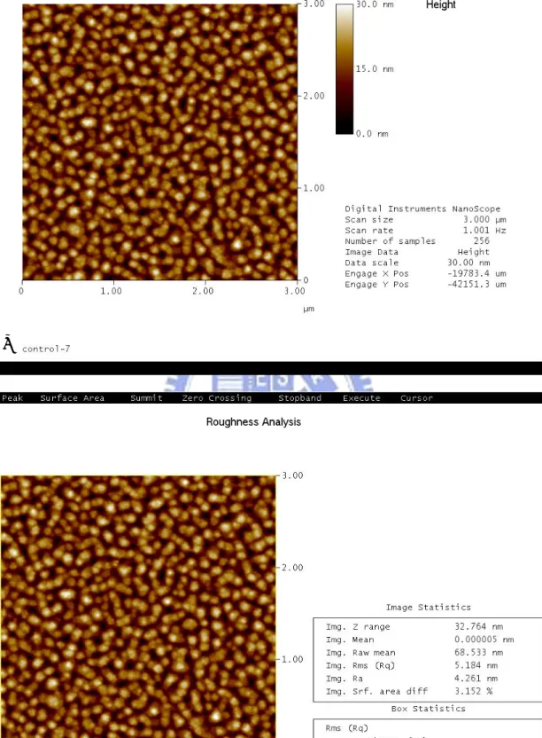
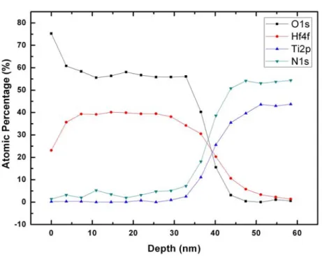
2.2.4 Atomic force microscope (AFM)
The atomic force microscopy (AFM) is a very good tool to research the surface roughness and surface morphology. We use an AFM made by digital instruments whose model is Nano-Scope E. The root mean square (RMS) value of roughness of the film is automatically calculated by the AFM software.
2.2.5 X-ray photoelectron spectroscopy (XPS)
The X-ray spectroscopy is used to characterize the binding energy and the compositions of the thin film. The electron binding energy is influenced by its chemical surroundings making binding energy suitable for determining chemical states. XPS is a surface-sensitive method because the emitted photoelectrons originate from the upper 0.5~5nm of the sample, just as Auger electrons do, despite the deeper penetration of the primary X-rays compared to a primary electron beam.
2.3 Electrical characterization
The resistance switching behavior of the HfOx films was measured from I-V
relation using a computer-interfaced HP4156C. The measurements were done in sweep mode, with scanning from 0 to +V and 0 to –V for alleviating power damage [41]. During the measurements, a small current compliance (equipment limit 100mA ) was set with a constant voltage width to prevent the permanent breakdown of the oxide films.
Fig.2-1 The cross section of the Pd/HfOx/TiN device
Table 2- 1 Summary of Pd deposition parameters Substrate materials HfOx/ TiN/ SiO2/ Si
Deposition gas flow ratio Ar/ N2 = 24/ 0.5,12
Growth temperature Room temperature Background pressure < 3 x 10⁻⁵ Torr
Deposition pressure 7.6 mTorr Deposition power 110 W Deposition thickness 300Å
Table 2- 2 Summary of Pd / Al deposition parameters Substrate materials HfOx/ TiN/ SiO2/ Si
Deposition gas flow ratio Ar/ N2 = 24/ 0.5,12
Growth temperature Room temperature Background pressure < 3 x 10⁻⁵ Torr
Deposition pressure 7.6 mTorr Deposition power 110 W Deposition thickness 300Å
Chapter 3 Results and Discussion
3.1 Structural analysis
It should be understood that the performance of nonvolatile memory depend on the electrical properties, the yield of nonvolatile memory depend on the physical properties. In the following sections, we will introduce the physical measurements and analyses include X-ray diffraction analysis, scanning electron microscope analysis, atom force microscope analysis, and X-ray photoelectron spectrometer analysis. The measurements are used to see the pyrolysis temperature, crystallization temperature, preferred orientation, grain size, morphology of surface and cross-section, the surface roughness degree, the content of major element, and the bonding energy. Besides, the physical properties measurement can help us to find the better fabrication parameters.
3.1.1 Film thickness and composition
Fig 3-1 shows the SEM micrograph of cross-sectional structure of an as deposited HfOx film. The HfOx films have average thickness of 36nm. Fig 3-2 shows
the AFM of step height of an as deposited HfOx film. These errors are cut
fragmentations or instrument to cause. The HfOx films have average thickness of 33.8
nm. A rough thickness between the HfOx film and the TiN metal is observed. This is
attributed to the rough surface of the TiN metal, which has a columnar structure, as shown in the SEM image. The roughness of the HfOx film on TiN was measured show
Fig 3-3. As shown in Fig 3-3(b), the rms surface roughness over a scanning area of 3000 x 3000 μm2 is 51.84Å. The roughness of the HfOx film Fig 3-4 shows the SEM,
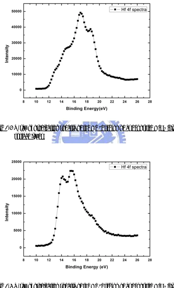
prove the surface of roughness. The depth profile of the chemical composition of HfOx films measured by XPS is shown in Fig 3-5. The atomic ratio of oxygen to
hafnium (O: Hf) inside the HfOx film is found to be about 1.5, which suggests that the
HfOx film is nonstoichichiometric. In Fig 3-6, the binding energy of Hf 4f was 17 and
17.6eV (Hf 4+). This indicates that surface layer is mainly composed of stoichiometric HfO2. Because the sampling depth of XPS is deep, thus, a low binding energy feature
seems to originate from sublayers. In Fig 3-7, the interface region the binding energies were 14.2 and 15.6eV (Hf 0). There is more oxygen content of surface, so the interface forming binding energy is different from surface.
3.1.2 Crystalline structure
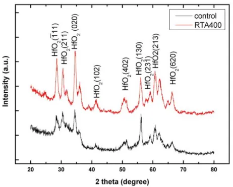
Fig 3-8 shows the X-ray diffraction patterns of as-deposited HfOx films. The
films grown were polycrystalline and consisted mainly of the monoclinic HfOx [42]
phase, which is the stable polymorph of HfOx under normal conditions. [43, 44]
Fig. 3-9 shows the XRD analysis in thermal treatment temperature, find increases HfO2 intensity with through thermal treatment temperature. It means that the phase of
HfOx film will transform form amorphous into crystal after 400℃ thermal treatment.
The high temperature will increase the degree of crystallization. It can be observed clearly that the grain size become bigger at higher temperature.
3.2 Pd top electrodes Electrical property
In this section, what kind of experiment conditions can induce switching will be discussed. Including the nitrogen flow, thermal treatment temperature, then the analysis of the leakage current, switch voltage, conductivity ratio in different experiment conditions, and the leakage of different state will be explained by different mechanisms.
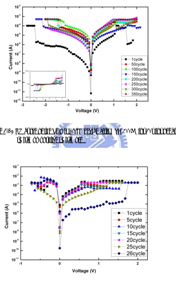
bipolar little cycle, in voltage sweeping (0→-V) and (0→+V)mode the voltage and leakage current characteristic was unstable. The sample ratio is 250 time. The inset of Fig 3-10 exhibits the linear curve of switching, the H-state is lower compliance current, but the L-state is larger current. The sample has larger resistance ratio, but the sample was not operating positive switch on, negative switch off electrical property. In this investigation we carried out different treatment. The first section, we make the treatment of different annealing time. As observed in Fig. 3-11, the I-V curves of the Pd/ HfOx/ TiN films after RTA 400℃ for 30sec, in voltage sweeping (0→-V) and
(0→+V)mode. In the RTA 400℃ for 30sec sample cycle more than without treatment sample, but operating ratio is reduces 250 to 25 time. The H-state reduces of the operating voltage to thermal treatment temperature. The H-state and L-state were operating to stable after treatment temperature, but the L-state main switch is slow. Fig. 3-11 shows switch cycle vs. voltage. The voltage change has 2V, a large amount of voltage changes, showing an unstable state. Because the Pd/HfOx/TiN device is unstable and less switching cycle, we did a thermal treatment. The inset of Fig 3-12 exhibits the linear curve of switching, the H-state current change larger than without treatment sample. Fig 3-13 shows I-V curve of the Pd/HfOx/TiN device after RTA
400℃ 30s for positive switch on, negative switch off. The sample was without treatment only negative switch on characteristic. The thermal treatment was increasing operating cycle, and operating voltage is low. The operating ratio was 5 time. Fig 3-14 shows I-V curve of the Pd/HfOx/TiN device after RTA 400℃ for 1min.
From Fig 3-9 the XRD analysis, it is easy to find when the thermal treatment temperature at 400℃, the HfOx film increasing crystalline phase intensity will have
the phase change phenomenon. The inset of Fig 3-14 shows the operating voltage is more stable than without treatment sample, but operating current is large. Fig 3-15 shows I-V curve of the Pd/HfOx/TiN device after RTA 400℃ 1min for positive switch
on, negative switch off. The sample transfer characteristic is better than thermal treatment 400℃ 30s, and resistance ratio is large than thermal treatment 400℃ 30s. The sample resistance ratio is 20 time. Fig 3-16 shows comparison thermal treatment of the Pd/HfOx/TiN device.Annealing at 400℃ is useful to reduce operation voltage
which might be enhancement of the crystallinity to attain a stable switching behavior with high endurance. Long thermal treatment time has an intensity stronger crystallinity. Fig 3-17 shows comparison sample of thermal treatment as Pd initial forming. The thermal treatment is reduced operating voltage effectively, but leakage current has no change. Lower voltage can form current paths with the thermal treatment. Fig. 3-18 shows compare different thermal treatment time of thermal treatment. The OFF-state was decrease operating voltage with increasing thermal treatment time, but the ON-state thermal treatment time increasing with operating voltage. The resistance ratio is decrease with increasing thermal treatment time, the RTA 1min resistance ratio only remain 10 times. The resistance ratio has large without thermal treatment, but operating cycle times was less. Increasing thermal treatment with switch cycle time effective. Fig. 3-19, 20 shows nitrogen flow is 0.5 sccm and 12 sccm before deposition Pd layer, respectively. The nitrogen can be reduced leakage current and increasing operating the number of times. In this study, we present results the effect of nitrogen and thermal treatment from negative switching-on, positive switching-off. Clearly, the findings indicate that nitrogen and thermal treatment has a positive effect on operation cycle time and leakage current. Fig 3-21 shows comparison nitrogen different flow with deposition Pd initial forming. The switch has lower leakage current with nitrogen flow treatment. Fig 3-22, 23 shows nitrogen flow 0.5sccm 20s and 12sccm 20s to different thermal treatment, the thermal treatment can increase nitrogen effective. Table 3-1, and Table 3-2 shows comparison Pd/HfOx/TiN sample different treatment negative switch on, and positive
switch on. Thermal treatment can positive switch on, negative switch off, but operating cycle is loss than negative switch on, positive switch off, and operating voltage and current are lager. The nitrogen flow treatment reduced leakage current, thermal treatment reduced operating voltage. These data lend support to that idea.
3.3 Pd/Al top electrodes Electrical property
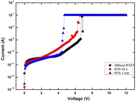
Fig. 3-24 shows Al layer of thickness, thicker of Al layer has lager leakage current because thicker Al layer have more interface defect. Thin Al layer has smaller leakage current because thinner Al layer has less interface defect, but without Al layer has less operation cycle time. Fig. 3-25 shows I-V curve of the Pd/Al/HfOx/TiN
device. Deposition Al interface layer is increasing positive turn on, negative turn off operation cycles because the switching is unstable, and operating cycle is fewer than negative turn on, positive turn off. Fig 3-26 shows compare Pd/Al/HfOx/TiN devices
different thermal treatment time by positive turn on, negative turn off. Before the positive turn on, negative turn off has no characteristic, but the Al interface layer is increasing voltage and the leakage current reduce for thermal treatment form improve the characteristic of operation. We were chosen the Al interface layer because it was active chemical reaction at the interfacial region. Fig 3-27 shows Pd/Al/HfOx/TiN
devices, the resistance ratio change less than 10times. The inset of Fig 3-27 exhibits the linear curve, the sample has switching stable and more operating cycle time, but resistance ratio is small. Fig 3-28 switch cycle vs. voltage of Pd/Al/HfOx/TiN device.
The switch voltage is 1V, it is a stable voltage and it has high endurance. It is very important for a nonvolatile memory device its memory state to keep long time its memory. The data storage time, called retention time, is a significant landmark. It means that how long the resistance values are kept in the two states. As shows in Fig.3-29, the retention time of the two states is at least over 18000 seconds and the
resistance ratio still keep over 100times, which dose not be affected by the operation of the memory readout.
Fig. 3-30 shows comparison nitrogen flow as 0.5 sccm different times before deposition Al layer to influence on operating the characteristic. The nitrogen wills deposition among interface and mends the defect. Long time of nitrogen flow will be reducing leakage current, but it will be increase voltage. This result has proved the appropriate nitrogen can reduce leakage current effectively. Fig 3-31 shows comparison different nitrogen flow as deposition 35 Å Al layer. The more nitrogen flow reduces little leakage current and resistance ratio change large, but it will be increase operating cycle times. The nitrogen flow influence leakage current and operating voltage because the nitrogen can reduce Al interface layer defect. The more nitrogen flow has lower leakage current, but the nitrogen makes the devices need large operating voltage. Fig 3-32 shows I-V curve of the Pd/AlN/HfOx/TiN device.
Nitrogen and aluminum was reaction form AlN insulating layer to increase the resistance ratio. Nitrogen treatment is beneficial for reduction of the leakage current to attain larger resistance ratio, but the operation voltage is unstable. Fig 3-33, 34 shows N2 6sccm 20s and N2 12 sccm 20s of the Pd/Al/HfOx/TiN device. The nitrogen
flow treatment can reduce of HRS leakage current effectively. Nitrogen and aluminum was reaction form AlN insulating layer to increase the switching on difficult. Fig 3-35 shows comparison different nitrogen flow before deposition 35 Å Al layers, the nitrogen flow influence leakage current and operating voltage. Appropriate nitrogen flow can reduce leakage current effectively. Reduce the leakage current as increases the nitrogen flow. At the nitrogen flow 12 sccm 20sec before deposition Al layer, receive the better operating has lower leakage current and operating voltage. Fig. 3-36 shows nitrogen flow different before deposition 35 Å Al layer for thermal treatment at 400℃ 30sec, the thermal treatment can accord with
nitrogen reduce leakage current effectively, and the nitrogen flow is associated with the leakage current. The nitrogen and thermal treatment can reduce leakage current. Fig. 3-37 shows nitrogen flow different before deposition 35 Å Al layer for thermal treatment at 400℃ 1min, long time of thermal treatment cause films redistribution increase grain size reduce grain boundary increase leakage current and reduce the operating voltage accord with result before. Fig 3-38 shows comparison Al 35 RTA resistance state, without thermal treatment resistance ratio is 2 time, the thermal treatment 400℃ 30s can increase resistance ratio ,but H-state and L-state has overlap, the thermal treatment 400℃ 1min resistance ratio is 100 time. The thermal treatment can increase resistance ratio effectively. Fig. 3-39 shows 12sccm 20 sec nitrogen flow for before deposition Al layer, and thermal treatment 400℃ 1min after deposition Al layer. The nitrogen was to reduce leakage current and thermal treatment reduces operating voltage. Excessive of nitrogen to long-time can get better stable operation through the thermal treatment, the resistance ratio large than without treatment Pd/Al/HfOx/TiN device. As shows in Fig.3-40, the retention time of the two states is
at least over 30000 seconds and the resistance ratio still keep over 100times, which dose not be affected by the operation of the memory readout. Nitrogen 12 sccm 20s of Pd/Al/HfOx/TiN device in LRS and stability is relatively bad, unstable phenomenon that the main reason is made of nitrogen institute. Table 3-3, and Table 3-4 shows comparison Pd/Al/HfOx/TiN sample different treatment negative switch on, and
positive switch on. Deposition Al layer can positive switch on, negative switch off, but operating cycle is loss for positive switch on with different treatment. Positive switch on operating voltage is lager.
3.4 Fitting leakage current property
Form the physics of semiconductor devices, there are six different basic conduction processes in semiconductors: Schottky emission, Frenkel-Poole emission, tunneling or field emission, space-charge-limited, Ohmic and Ionic conduction.
To understand and explain the conduction mechanisms, the current fitting of both H-state and L-state for I-V curve is performed. We consider that H-state is Frenkel-Poole emission as Pd/HfOx/TiN device, as showed in Fig. 3-41, which is
reasonable to be considered that L-state switching to H-state is the process of forming the current paths between the top electrode and bottom electrode. The current paths could be related to the arranging the order of point defects, such as oxygen vacancies and ionic defects associated with Hafnium atoms replaced. Electrons hop through the defects within the doped HfOx films. It is that the defects, composing the current
paths, trap the electrons causes some ruptures of the current paths. However, at the same time, other current paths have chances to be formed again, which increase the conduction current within the transition region. Excessive of the nitrogen flow and without nitrogen treatment current fitting is Frenkel-Poole emission. The Frenkel-Poole emission equation is Vexp(2 )
kT q T V a J ≈ − φB .
As showed in Fig.3-42, that L-state is Ohmic conduction. I - V characteristics exhibiting the I V correlation is Ohmic (slope = 1). Which is reasonable to be considered that H-state switching to L-state is the process of ruptured the current paths between the top electrode and bottom electrode. The conduction mechanisms dominating in the H-state is Frenkel-Poole emission and L-state is Ohmic conduction. Fig 3-43 show the different thermal treatment at H-state, as the without thermal treatment and thermal treatment current fitting is Frenkel-Poole emission, switching conduction mechanisms with the structure which has changed by thermal treatment.
Fig 3-44 show L-state through thermal treatment changed switching conduction mechanisms from Ohmic conduction. The Pd/HfOx/TiN device whether thermal
treatment or nitrogen flow treatment, the H-state is dominated by Frenkel-Poole emission, the L-state is dominated by Ohmic conduction. Fig 3-45 shows as different nitrogen flow treatment before deposition Al interface layer H-state changed switching conduction mechanisms, the switching conduction mechanisms is same from Pd. The switching conduction current fitting is Frenkel-Poole emission. Fig 3-46 show deposition Al layer H-state without nitrogen flow treatment and nitrogen flow treatment is dominated by Ohmic conduction. Fig 3-47 show deposition Al layer H-state different thermal treatment, the switching conduction mechanisms is Frenkel-Poole emission. Whether it is nitrogen flow or thermal treatment H-state is Frenkel-Poole emission. Fig 3-48 show deposition Al layer L-state different thermal treatment is Ohmic conduction. The thermal treatment does not influence the transfer characteristic.
It is proved again that the H-state dominated by forming of the current paths. While a current path is formed, the electrons prefer to pass through the new-formed current path, which causes other paths to be formed with little chance. The small variation of the resistance of the H-state could be explained clearly. But, the larger variation of the resistance of the L-state is relative to the random electron-trapping in the turn-off process.
From the I-V curve that has been shown, the leakage current density of the OFF/ON state shows at both positive and negative voltage. As the same reason, the mechanism of the device was conjectured due to interface. Besides, at the high temperature, the current of the L-state significantly increases more than that of the H-state. It may be due to the electrons more difficult to be trapped at the higher temperature during the OFF process, which leads the fewer current paths to be
ruptured. Have proved the Al, nitrogen, thermal treatment will change and switching conduction mechanisms to the attitude characteristic.
Fig 3-1 SEM cross-sectional structure of as deposited HfOx film
(a)
(b)
Fig 3-4 SEM top view of as deposited HfOx film
Fig 3-6 X-ray photoelectron spectra of the Hf 4f region of as deposited HfOx films in
surface layer
Fig 3-7 X-ray photoelectron spectra of the Hf 4f region of as deposited HfOx films in
Fig 3-8 X-ray diffraction patterns of as-deposited HfOx films
Fig 3-10 I-V curve of the Pd/HfOx/TiN device
Fig 3-12 I-V curve of the Pd/HfOx/TiN device after RTA 400℃ for 30s for negative
switch on positive switch off
Fig 3-13 I-V curve of the Pd/HfOx/TiN device after RTA 400℃ for 30s for positive
Fig 3-14 I-V curve of the Pd/HfOx/TiN device after RTA 400℃ for 1min
Fig 3-15 I-V curve of the Pd/HfOx/TiN device after RTA 400℃ 1min for positive
Fig 3-16 comparison thermal treatment of the Pd/HfOx/TiN device
Fig 3-18 comparison sample of thermal treatment at various RTA times
Fig 3-20 I-V curve as N2 12sccm 20s before deposition Pd layer
Fig 3-22 comparison sample as N2 0.5sccm 20s of thermal treatment at various
RTA times
Fig 3-23 comparison sample as N2 12 sccm 20s of thermal treatment at various
Fig 3-24 comparison Al layer of thickness
Fig 3-25 I-V curve of the Pd/Al/HfOx/TiN device for positive switch on negative
Fig 3-26 I-V curve of the Pd/Al/HfOx/TiN device as different thermal treatment
time
Fig 3-28 switch cycle vs. voltage of Pd/Al/HfOx/TiN device
Fig 3-30 comparison nitrogen flow 0.5sccm different time at deposition 35Å Al
Fig 3-32 I-V curve of the Pd/AlN/HfOx/TiN device
Fig 3-34 I-V curve as N2 12sccm 20s of the Pd/Al/HfOx/TiN device
Fig 3-36 comparison nitrogen different flow with deposition 35Å Al RTA 30s
Fig 3-38 comparison Al 35 RTA resistance state
Fig 3-39 I-V curve of the Pd/Al/HfOx/TiN device as N 12sccm 20s after RTA
Fig 3-40 Retention properties of RLow and RHigh at room temp
Fig. 3-41 the current fitting of H-state as Pd/HfOx/TiN device as different nitrogen
Fig. 3-42 the current fitting of L-state as Pd/HfOx/TiN device as different nitrogen
flow I-V curve
Fig. 3-43 the current fitting of H-state as Pd/HfOx/TiN device as different thermal
Fig. 3-44 the current fitting of L-state as Pd/HfOx/TiN device as different thermal
treatment I-V curve
Fig. 3-45 the current fitting of H-state as Pd/Al/HfOx/TiN device as different
Fig. 3-46 the current fitting of L-state as Pd/Al/HfOx/TiN device as different
nitrogen flow I-V curve
Fig. 3-47 the current fitting of H-state as Pd/Al/HfOx/TiN device as different
Fig. 3-48 the current fitting of L-state as Pd/Al/HfOx/TiN device as different
Table 3-1 comparison Pd/HfOx/TiN sample different treatment negative
switch on
Origin RTA 30s RTA 1min N20.5sccm 20s N2 12sccm 20s Current 200μA 500μA 1mA 500μA 1mA
Voltage >2V ~1.5V ~1V <1.5V ~1V Endurance 8 350 300 200 100 ratio 250 25 1 5 10 N2 0.5 sccm 20s N2 0.5 sccm 20s RTA 30s N20.5 sccm 20s RTA 1min Current 200μA 500μA 200μA
Voltage ~1V ~1.5V ~1V Endurance 200 250 100 ratio 50 10 10 N2 12 sccm 20s N2 12 sccm 20s RTA 30s N2 12 sccm 20s RTA 1min Current 100μA 100μA 100μA
Voltage ~1V ~4V <2V
Endurance 100 200 325
ratio 10 10 10
Table 3-2 comparison Pd/HfOx/TiN sample different treatment positive
switch on
Origin RTA 30s RTA 1min N20.5sccm 20s N2 12sccm 20s
Current x 2mA 2mA x x
Voltage x ~2V >4V x x
Endurance x 52 50 x x ratio x 5 20 x x
Table 3-3 comparison Pd/Al/HfOx/TiN sample different treatment
negative switch on
Origin RTA 30s RTA 1min N20.5sccm 20s N26sccm 20s N2 12sccm 20s
Current ~1mA ~500μA ~50μA ~500μA ~500μA ~500μA Voltage <1V <1.5v ~3.5v <2V <2V <2v Endurance 1500 75 13 30 5 75 ratio 10 150 2x10⁴ 103 103 4x10⁴ N2 6 sccm 20s N2 6 sccm 20s RTA 30s N2 6 sccm 20s RTA 1min Current 500μA 50μA 200μA
Voltage ~2V ~1.5V ~1.5V Endurance 10 20 25 ratio 50 10 10 N2 12 sccm 20s N2 12 sccm 20s RTA 30s N2 12 sccm 20s RTA 1min Current 10mA 10μA 10μA
Voltage ~2.5V ~2V ~1.5V
Endurance 30 11 25
ratio 10 10 10
Table 3-4 comparison Pd/Al/HfOx/TiN sample different treatment
positive switch on
Origin RTA 30s RTA 1min N2 0.5sccm 20s N2 6 sccm 20s N2 12sccm 20s
Current ~1mA ~500μA ~50μA ~500μA ~500μA ~500μA
Voltage <1V <1.5v ~3.5v <2V <2V <2v
Endurance 1500 75 13 30 5 75
Chapter 4 Conclusions
In this thesis, bipolar resistive switching characteristics could be observed on our all HfOx film by switching to LRS state by negative bias and to HRS state by positive
bias. Both Pd/HfOx/TiN and Pd/Al/HfOx/TiN show the similar tendency to nitrogen
treatment, thermal treatment, and the combined (nitrogen + thermal) treatment. Thermal treatment can reduce operation voltage effectively, but it will increase HRS current owning to higher crystallinity of HfOx film. The nitrogen flow treatment can reduce of HRS current effectively, especially on Pd/Al/HfOx/TiN sample, but it will
increase operation voltage and partially degrade the stable switching properties. Adding slight nitrogen gas in the beginning of Al electrode deposition has more obvious benefits to reduce HRS current than Pd, which might be due to difference of the metal characteristics. Combining the nitrogen and RTA treatment together on our Pd/Al/HfOx/TiN film, both the advantages of reliable switching properties and lower
HRS current could be obtained. Adding nitrogen during Pd electrode deposition has no obvious benefits to reduce leakage current. By an additional thermal treatment, the leakage current at HRS could be slight reduced. Inserting Al thin layer in the Pd/HfOx
interface greatly improves the resistive switching characteristics of HfOx/TiN RRAM
indicating that the interface is a critical issue for resistive switching. We believe that interface and bulk are both critical to the resistive switching characteristics, and the characteristics of interface or bulk could be modified by top electrode or thermal treatment. Possible model of our bipolar-switched HfOx film is the oxygen migration
between TiN and HfOx film. TiN bottom electrode serves as an oxygen reservoir
during SET process by negative bias, and re-oxidizes with HfOx film under positive
bias during RESET process. Several factors are still needed being discussed such as forming process, operation mode, current compliance, and current values to
Reference
[1] D. Kahng and S. M. Sze, “A floating gate and its application to memory devices,” Bell Systems Technical Journal, vol. 46, p. 1283, 1967.
[2] W. W. Zhuang, W. Pan1, B. D. Ulrich, J. J. Lee1, L. Stecker1, A.Burmaster1, D. R. Evans, S. T. Hsu, M. Tajiri, A. Shimaoka, K. Inoue, T.Naka, N. Awaya, K. Sakiyama, Y. Wang, S. Q. Liu, N. J. Wu, and A.Ignatiev, “Novell Colossal Magnetoresistive Thin Film NonvolatileResistance Random Access Memory (RRAM)”, in IEDM Tech. Dig., 2002,pp. 193-196.
[3] M. Lines and A. Glass, “Principles and applications of ferroelectrics and \ related devices”, Clarendon Press, Oxford, 87(1977).
[4] J. Daughton, “Magnetoresistive Random Access Memory (MRAM)”, NVE Web page < http://www.nve.com/>, (2000)
[5] E. Y. Chen, S. Tehrani, T. Zhu, M. Durlam, and H. Goronkin, “Submicron spin valve magnetoresistive random access memory cell”, J. Appl. Phys. 81, 3992(1997).
[6] S. Tehrani, E. Chen, M. Durlam, M. DeHerrera, J. M. Slaughter, J. Shi, and G. Kerszykowski, “High density submicron magnetoresistive random access memory”, J. Appl. Phys. 85, 5822(1999).
[7] D.D. Tang, P.K. Wang, V. S. Speriosu, S. Le, R.E. Fontana, S. Rishton, “An IC process compatibie nonvolatile magnetic RAM”, IEDM Tech. Dig. 997(1995). [8] S. Tehrani, E. Chen, M. Durlam, T. Zhu, and H. Goronkin, “High density
nonvolatile magnetoresistive RAM”, IEDM Tech. Dig. 193(1996). [9] J. De Boeck and G. Boughs, IEC, permission of IEEE, (1999).
[10] S. Parkin, “Origin of enhanced magnetoresistance of magnetic multilayers: spin-denpendent scattering from magnetic interface states”, Phys. Rev. Lett. 71, 1641(1993).
[11] M. N. Baibich, J. M. Broto, A. Fert, F. Nguyen Van Dau, F. Petroff, P. Eitenne, G. Creuzet, A. Friederich, and J. Chazelas, “Giant magnetoresistance of (001)Fe/(001)Cr magnetic superlattices”, Phys. Rev. Lett. 61, 2472(1988).
[12] B. Prince, “Application for emerging memories”, Memory Strategies International, (2001).
[13] W. J. Gallagher, S. Parkin, Yu Lu, X. P. Bian, A. Marley, K. P. Roche, R. A. Altman, S. A. Rishton, C. Jahnes, T. M. Shaw, and Gang Xiao, “Microstructured magnetic tunnel junctions” J. Appl. Phys. 81, 3741(1997).
[14] S. Parkin, K. P. Roche, M. G. Samant, P. M. Rice, R. B. Beyers, R. E. Scheuerlein, E. J. O’Sullivan, S. L. Brown, J. Bucchigano, D. W. Abraham, Yu Lu, M. Rooks,P. L. Trouilloud, R. A. Wanner, and W. J. Gallagher, “Exchange-biased magnetic tunnel junctions and application to nonvolatile magnetic random access memory”, J. Appl. Phys. 85, 5828(1999)
[15] S. R. Ovskinsky, “Reversible Electrical Switching Phenomena in Disordered Structures”, Phys. Rev. Lett. 21, 1450(1968).
[16] S. Kim, I. Byun, I. Hwang, J. Kim, J. Choi, B. H. Park, S. Seo, M. J. Lee, D. H. Seo, D. S. Suh,Y. S. Joung, and I. K. Yoo: Jpn. J. Appl. Phys. 44 (2005) L345. [17] C. Rossel, G. I. Meijer, D. Bre´maud, and D. Widmer, “Electrical current
distribution across a metal-insulator-metal structure during bistable switching,” J. Appl. Phys., vol. 90, pp.2892-2898, 2001
[18] S. Tsui, A. Baikalov, J. Cmaidlka, Y. Y. Sun, Y. Q. Wang, Y. Y. Xue, C. W. Chu, L. Chen, and A. J. Jacobson, “Field-induced resistive switching in metal-oxide interface,” Appl. Phys. Lett., vol. 85, pp.317-319, 2004.
[19] A. Baikalov, Y. Q. Wang, B. Shen, B. Lorenz, S. Tsui, Y. Y. Sun, Y. Y. Xue, and C. W. Cju, “Field-driven hysteretic and reversible resistive switch at the Ag-Pr0.7Ca0.3MnO3 interface,” Appl, Phys. Lett., vo;. 83, pp.957-959, 2003.
[20] T. Fujii, M. Kawasaki, A. Sawa, H. Akoh, Y. Kawazoe, and Y. Tokura, Appl. Phys. Lett. 86, 012107 "2005#.
[21] K. Jung, H. Seo, Y. Kim, H. Im, J. P. Hong, J.-W. Park, and J.-K. Lee, Appl. Phys. Lett. 90, 052104 "2007#.
[22] U. Russo, D. Ielmini, C. Cagli, A. L. Lacaita, S. Spiga, C. Wiemer, M. Perego, and M. Fanciulli, Tech. Dig. - Int. Electron Devices Meet. 2007,775.
[23] J. B. Yun, S. Kim, S. Seo, M.-J. Lee, D.-C. Kim, S.-E. Ahn, Y. Park, J. Kim, and H. Shin, Phys. Status Solidi 1, 280 "2007#.
[24] Q. Liu, W. Guan, S. Long, R. Jia, M. Liu, and J. Chen, Appl. Phys. Lett. 92, 012117 "2008#
[25] S. Seo, I. S. Byun, M. J. Lee, D. C. Kim, S. E. Ahn, B. –H Park, Y. S. Kim, I. K. Yoo, I. R.Hwang, S. H. Kim, J. –S. Kim, J. S. Choi, J. H. Lee, and S. H. Jeon: Appl. Phys. Lett. 87 (2005)263507.
[26] C. Y. Lin, C. Y. Wu, C. Y. Wu, T. C. Lee, F. L. Yang, C. Hu, and T. Y. Tseng: IEEE Electron Device Lett. 28 (2007) 366.
[27] C. B. Lee, B. S. Kang, A. Benayad, M. J. Lee, S. –E. Ahn, K. H. Kim, G. Stefanovich, Y. Park, and I. K. Yoo: Appl. Phys. Lett. 93 (2008) 042115.
[28] H. Y. Lee, P. S. Chen, C. C. Wang, S. Maikap, P. J. Tzeng, C. H. Lin, L. S. Lee, M. J. Tsai: Jpn. J. Appl. Phys. 46 (2007) 2175.
[29] H. Y. Lee, P. S. Chen, T. Y. Wu, C. C. Wang, P. J. Tzeng, C. H. Lin, F. Chen, M. J. Tsai, C. Lien: Appl. Phys. Lett. 92 (2008) 142911.
[30] S. Lee, W. G. Kim, S. W. Rhee, and K. Yong: J. Electrochem. Soc. 155 (2008) H92.
[31] I. Inoue, et.al. “Strong electron correlation effects in non-volatile electron memory devices”, NVMTS, p.131 (2005).