國 立 交 通 大 學
電子工程學系電子研究所
碩 士 論 文
有太陽能電池之仿雙載子電晶體為基礎低功率
可植入式矽視網膜晶片設計
The Design of Low Power Implantable Pseudo-BJT-Based
Silicon Retina with Solar Cells for Artificial Retinal
Prostheses
研 究 生:鄭淑珍 Felice Cheng
指導教授:吳重雨 Chung-Yu Wu
有太陽能電池之仿雙載子電晶體為基礎低功率可植入式矽
視網膜晶片設計
The Design of Low Power Implantable Pseudo-BJT-Based
Silicon Retina with Solar Cells for Artificial Retinal
Prostheses
研 究 生:鄭淑珍 Student: Felice Cheng
指導教授:吳重雨 Advisor: Chung-Yu Wu
國 立 交 通 大 學
電子工程學系電子研究所
碩 士 論 文
A Thesis Submitted toDepartment of Electronics Engineering and Institute of Electronics College of Electrical Engineering and Computer Sciences
National Chiao Tung University In partial Fulfillment of Requirements
for the Degree of Master
In
Electronics Engineering
July 2004
Hsinchu, Taiwan, Republic of China
有太陽能電池之仿雙載子電晶體為基礎低功率可植入式矽
視網膜晶片設計
研究生:鄭淑珍 指導教授:吳重雨 教授 國立交通大學 電子工程學系電子研究所 摘要 本論文描述一個有太陽能電池之偽載子電晶體為基礎低功率可植入式矽視 網膜。本論文突破了”底部式人工視網膜”視網膜細胞功能的限制,設計了一個同 時具有感光細胞,水平細胞及,雙極細胞功能的底部式人工視網膜。此外本論文 使用太陽能電池作為植入式視網膜的電源供應,此特徵使植入晶片於眼睛中可行 性大為增加。 利用台灣積體電路製造股份有限公司以 0.35 微米製程實現兩個人工視網膜 電路:一者為植入動物體用;另一者為儀器量測使用,並已自行量測完成。量測 結果顯示本架構實現了視網膜中感光細胞、水平細胞及、雙極細胞功的能。太陽 能電池量測結果顯示,在 2010 勒克斯照度下可提供 0.7 volt 電壓。利用太陽能 電池作為電源供應時,人工視網膜的功能也已量測證實為正確。The Design of Low Power Implantable Pseudo-BJT-Based
Silicon Retina with Solar Cells for Artificial Retinal
Prostheses
Student: Felice Cheng Advisor: Chung-Yu Wu
Department of Electronics Engineering and Institute of Electronics
National Chiao Tung University
ABSTRACT
In this thesis, the Pseudo-BJT-based silicon retina with solar cells for artificial
retinal prosthesis is designed and fabricated in 0.35um CMOS technology. The
Pseudo-BJT-based silicon retina possesses more functions of retinal cells than current
sub-retinal prosthesis. Besides, the solar cell is used to supply power to the artificial
retina and this feature makes implantation of the chip to the eye more feasible.
Two artificial retinal prostheses are fabricated with a standard TSMC 0.35um
CMOS process: one is for implantation and the other is for instrument measurement,
which is measured completely. The chip is demonstrated to have the functions of the
retinal cells: photoreceptors, horizontal cells and bipolar cells. The measured voltage
of the on-chip power supply, solar cell, is at least 0.7 volt under illumination of 2010
lux. The functions of the artificial retina have been demonstrated to be correct with
ACKNOWLEDGEMENTS
首先我要感謝我的指導老師吳重雨教授耐心的指導與鼓勵,使我
能夠順利的完成碩士學業。在吳教授循序漸進的殷殷教誨下,使我得
以獲得許多積體電路設計的專業知識,更在此過程中學習到面對壓力
與挑戰困難的精神,解決問題的方法。另外也要特別感謝林伯剛醫師
在醫學領域的指導與協助,讓這份跨領域的研究能夠順利完成。
在這段求學的過程中,積體電路與系統實驗室的給予了我完善的
硬體及軟體資源,讓我能夠順利的完成學業,感謝學長姐們努力經營
實驗室,讓實驗室如同我第二個家。更感謝實驗室學長姐,施育全,
林俐如,江政達,王文傑,陳勝豪等的細心指導;感謝實驗室同儕們
的陪伴,讓我這段實驗室的歲月過的不僅充實也很溫馨有趣。
此外我要感謝我的摯友,陳蓉萱小姐與謝文芩小姐。感謝妳們的
陪伴與關懷,使我的生活增色不少。
另外,我還要特別感謝陪伴我的陳建宏先生。因為你的支持與關
心,讓我能夠在低潮與壓力中堅持下去,從跌倒中站起來,勇敢的朝
自己的目標繼續邁進。
最後,我要致上我最深的感謝給予我父親鄭仁奎先生,母親孫美
容女士,姊姊鄭淑小姐,哥哥鄭義勳先生,弟弟鄭義宏先生。沒有你
們的無私的付出與關懷,我無法完成今天的成就。感謝上天將你們賜
與我,讓我有幸福的家庭。
鄭 淑 珍
誌於 風城交大
九十三年 仲夏
有太陽能電池之偽雙載子電晶體為基礎低功率可植入式矽
視網膜晶片設計
The Chip Design of Low Power Implantable
Pseudo-BJT-Based Silicon Retina with Solar Cells for
Artificial Retinal Prostheses
CONTENTS
ABSRACT (CHINESE) i ABSRACT (ENGLISH) ii ACKNOWLEDGEMENT iii CONTENTSEDGEMENT iv TABLE CAPTIONS viFIGURE CAPTIONS vii
CHAPTER 1 INTORDUCTION 1.1 BACKGROUND 1
1.2 REVIEW ON HARDEARE IMPLEMENTATIONS CONCERNING THE RETINA 2
1.2.1 Hardware Implementations Designed from The Biological Model of The Retina 2
1.2.2 Epi-Retinal Prosthesis 4
1.2.3 Sub-Retinal Prosthesis 5
1.3 REVIEW ON POWER SUPPLY ISSUE IN ARTIFICIAL RETINAL PROSTHESIS 5
1.4 MOTIVATIONS 6
CHAPTER 2 THE ARCHITECTURE OF VERTERATE RETINA 2.1 INTRODUCTION 11
2.2 THE PHOTORECEPTOR CELLS 11
2.4 THE BIPOLAR CELLS 12
2.5 THE AMACRINE CELLS 13
2.6 THE GANGLION CELLS 14
2.7 A SUMMARY OF THE FUNCTIONAL ORGANIZATION OF THE RETINA 14
CHAPTER 3 THE DESIGN, CHARACTERISTICS AND ANALYSIS OF ARTIFICIAL RETINA 20
3.1 THE CHARACTERISTICS OF PN JUNCTION DIODE AS ARTIFICIAL RETINA 22
3.2 ANALYSIS OF THE PSEUDO-BJT-BASED SILICON RETINA 23
3.3 THE POWER SUPPLY ISSUE OF IMPLANTED SILICON RETINA 23
3.4 SIMULATION RESULTS 24
CHAPTER 4 EXPERIMENTAL RESULTS 4.1 LAYOUT DISCREPTION 51
4.2 MEASUREMENT RESULTS 51
4.3 DISSCUSSIONS 52
4.4 SUMMARY 53
CHAPTER 5 CONCLUSIONS AND FUTURE WORKS 5.1 MAIN RESULTS OF THIS THESIS 74
5.2 FUTURE WORKS 74
TABLE CAPTIONS
CHAPTER 3
Table 3.1 The simulation condition of Fig. 3.16. Table 3.2 The simulation condition of Fig. 3.17.
Table 3.3 The power supply rejection ratio of the proposed silicon retina.
Table 3.4 The simulated condition of the power supply rejection ratio in Table 3.3. Table 3.5 The components in Fig.3.19 and the corresponding meaning.
CHAPTER 4
Table 4.1 The luminance of the light on the chip under different light source strength.
Table 4.2 The post-simulation condition and measurement condition for Fig. 4.10 (a).
Table 4.3 The post-simulation condition and measurement condition for Fig. 4.10 (b).
Table 4.4 The post-simulation condition and measurement condition for Fig. 4.13.
Table 4.5 The required solar cell area under different illumination but fixed photocurrent of photodiode.
Table 4.6 The required solar cell area consideration the focusing of the lens. Table 4.7 The summary of the chip for instrument measurement.
FIGURE CAPTIONS
CHAPTER 1
Fig. 1.1 The Human Eye.
Fig. 1.2 A Conceptual Epi-Retinal Prosthetic System.
Fig. 1.3 The Typically Functional Implantable Epi-Retinal Microsystem. Fig. 1.4 The Sub-Retinal Implant.
CHAPTER 2
Fig. 2.1 The schematic diagram of the retinal circuitry of the vertebrate retinas. Fig. 2.2 Intracellular recording from the mudpuppy retina showing the difference in
response of a given cell type to a 100-μm spot and to annuli of 0.5 and 1.0 mm in diameter, all at the same intensity.
Fig. 2.3 Two schemes suggesting how direction-sensitive responses may be mediated by excitatory and inhibitory amacrine cells in the retina. Fig. 2.4 Summary scheme of the synaptic interactions that occur in the retina and
that underlie the receptive field properties of the on-center, off-center, and on-off ganglion cells.
CHAPTER 3
Fig. 3.1 Visualization of light absorption, electron-hole creation, and the light-induced current in a pn junction diode.
Fig. 3.2 Photodiode I-V characteristics.
Fig. 3.3 Four different diode array designed as artificial retina.
Fig. 3.4 A p+-n-well diode and a current mirror with current gain of 8 formed by PMOS as the artificial retina.
Fig. 3.5 The circuit diagram of (a) npn pseudo-BJT (PBJT) and its device symbol, (b) pnp pseudo-BJT (PBJT) and its device symbol.
Fig. 3.6 The pixel circuit of the proposed low-power implantable PBJT-based retina circuit.
Fig. 3.7 The architecture of 2-D retinal array.
Fig. 3.8 The I-V characteristics of a teskey of pn junction diode.
Fig. 3.9 Characteristic I-V curves of the teskey and a load line of the proposed circuits.
Fig, 3.10 One block of solar cell as power supply. Positive and negative power supply formed by 2 series-wound solar cells and 150 paralleled solar cells respectively exploiting the tissue potential varying from -60mV to -35mV.
Fig. 3.11 The smoothing function of pseudo-BJT-based silicon retina simulated under the photocurrent of (a) 1nA, (b) 10nA.
Fig. 3.12 The edge-extract function of pseudo-BJT-based silicon retina simulated under the photocurrent of (a) 1nA, (b) 10nA.
Fig. 3.13 The simulated output current waveform of a cell in a linear silicon retina array with the moving-object image incident on the array.
Fig. 3.14 (a) The 2-dimensional pattern with the photocurrent incident on 16 pixels locating at the center of the chip of 64 pixels (8x8). The light window simulated in 1 nA is located at row 3rd to row 6th and column 3rd to column 6th. (b) The corresponding edge-extract output current.
Fig. 3.15 (a) The edge-extract function for the proposed Pseudo-BJT-based silicon retina (32 pixels). The light is incident on the 12th to the 19th pixels, while the photocurrent is simulated in two different current levels, that is, 25nA (a) and 125nA (b). The corresponding voltage of Vsmooth is 0.9volt and 1volt, respectively.
Fig. 3.16 (a) The edge-extract function under different smoothing biases. A linear silicon retina array with 32 pixels is considered. The simulation condition is shows in Table 3.1.
Fig. 3.17 The flash reaction of the proposed silicon retina in a linear array with 32 pixels. There is overshooting when the light turns on, but this phenomenon becomes unapparent when the input photocurrent decreases to 25nA. Fig. 3.18 The pre-simulation and post-simulation result of the flash reaction of the
proposed silicon retina. The simulation condition is the same as Table 3.2. Fig. 3.19 The parasitic N-well capacitor in the pixel circuit.
Fig. 3.20 The comparison of simulation results with (a), and without parasitic N-well capacitor (b).
Fig. 3.22 The simulated flash reaction of solar cell.
CHAPTER 4
Fig. 4.1 (a) The photograph of the basic cell in the 2-D array, (b) the photodiode in single pixel, (c) solar cells as power supply in the chip for implantation and (d) the photograph of the whole implantation chip.
Fig. 4.2 (a)The photograph of the whole implantation chip and (b) the decoder
Fig. 4.3 (a) The measurement setup chart. (b)The cross-sectional drawing of the setup for the chip.
Fig. 4.4 The power (a) and the luminance (b) of the light on the chip versus different input light power under this setup condition.
Fig. 4.5 The I-V characteristics of the solar cell in the chip for instrument measurement. The solar area is 1120umx490um.
Fig. 4.6 The open circuit voltage(a) and the short circuit current (b) of the solar cell in the chip for instrument measurement.
Fig. 4.7 The flash light reaction of the solar cell in the chip for instrument measurement. The light source is yellow LED with light intensity of 212lux.
Fig. 4.8 The spectrum analysis of photodiode.
Fig. 4.9 The photograph of the chip for instrument measurement with opaque material shielding from light to form the light and dark boundary. Fig. 4.10 The post-simulated waveform and the measured waveform under light
intensity of 736 lux and smooth voltage of 0.9 volt (a), and under light intensity of 3460 lux and smooth voltage of 1 volt.
Fig. 4.11 The measured waveform of the 2-D array under light intensity of 3460 lux and smooth voltage of 1 volt.
Fig. 4.12 The response of the chip under flashlight. The flashlight intensity is 3460 lux and the smooth voltage is 1 volt.
Fig. 4.13 The measured waveform of the chip for instrument measurement. The light intensity is 3460 lux while the smooth voltage is 1 volt.
Fig. 4.14 Typical diffraction and slit interference pattern.
CHAPTER 1
INTORDUCTION
1.1 BACKGROUND
Vision is one of the most important sensory organs and thus losing vision can bring one endless torments. Currently, over 10,000,000 people worldwide are blind because of photoreceptor loss or other cells loss in the retina [1]. Although medicine and ophthalmology today is well developed, some of the retinal degenerative diseases cannot be treated yet, such as retinitis pigmentosa (RP) and advanced age-related macular degeneration (AMD). Retinitis Pigmentosa has an incidence of 1 in 4000 live births, whereas 200,000 eyes are blinded each year by age-related macular degeneration. Thus, to restore vision with artificial retinal prosthesis draws considerable attention [2].
On the other hand, the operation underlying early visual processing have been studied for many years. A large number of well-studied mathematical algorithms for the early visual processing have been proposed [3]-[21]. However, there are several key problems in implementing these vision algorithms in digital hardware which is the most mature technology presently, to achieve real-time processing. The most common problems are the bottlenecks of computation and transmission. In a conventional digital computer, the computational bottleneck associated with the early visual processing is induced by the enormous complexity due to tremendous amount of data to be handled, rather than the calculation complexity. To overcome this problem, the new approach of implementing the visual processing completely based on the biological models is proposed and progressed significantly.
The vertebrate retina is a tiny sheet of neural tissue that locates at the back of the vertebrate eye chamber as shown in Fig. 1.1. It can perform two functions. Firstly, the photoreceptor is able to transducer the information of the optical image into neural signals. Secondly, the neural circuitry is able to abstract certain features of the visual world form the large number of photoreceptor signals and pass this information on to the brain via the optic nerve fibers. Because of its attractive functions, more and more research effort has been devoted to implement the operation of the retina in a physical semiconductor substrate. Various vision chips have been proposed to realize the functions of the retina [22]-[48].
elicited by electrical stimulations of neuronal tissues such as bipolar and/or ganglion cells of a retina. Fortunately the hypothesis has been verified via animal and human subject [2]. Critical question relating to the hypothesis include how many stimulations are required, and what are the electrical stimulus parameters (amplitude, duration, waveform, frequency) needed for each pixel in order to meet the safety and effectiveness constrains of the prosthesis. Answers to these questions greatly facilitate the optimal design, fabrication, fixation, and integration of and electrode array in a retinal prosthesis system and the power requirement of the prosthesis.
Based on the well development of silicon retina circuits and the verified hypothesis that light perception can be elicited by electrical stimulation of neural tissues, the artificial retinal prosthesis by implantable circuits can be developed and used to restore the vision of the blindness. There are two approaches for retinal implants, namely epi-retinal and sub-retinal implants. In an epi-retinal prosthesis, the prosthetic device is attached to the inner retinal surface so that the electrical signal directly stimulates the inner retina first. On the other hand, sub-retinal prosthesis places the implant in a space between neurosensory retinal and retinal pigment epithelium so that the electrical signal stimulates the outer retina first. The main advantage of the epi-retinal approach is to keep most of the electronics off the retinal space, in the vitreous cavity which greatly helps in dissipating the heat generated by the electronics. While the sub-retinal implant has the advantage of placing the electrodes closer to the bipolar cells and thus has a potential of reducing the stimulus threshold.
1.2 REVIEW ON HARDWARE IMPLEMENTATIONS CONCERNING THE RETINA
1.2.1 Hardware Implementations Designed from The Biological Model of The Retina
It is known that the retina of the vertebrate is an excellent intelligent image sensing and processing device. It performs the early vision process in a parallel manner to provide information for the brain to perceive the world. Because of its attractive functions, more and more research effort has been devoted to implement the operation of the retina in a physical semiconductor substrate [22]-[40]. The heart of the spatial image processing functions of the vertebrate retina which have been given considerable attention, are the adaptation to local and global light intensity, edge enhancement and edge detection. Various vision chips have been proposed to realize
the functions of the retina [22]-[40].
The heart of the spatial processing functions of the retina is the spatial smoothing functions. Image processing in the spatial domain is a very complicated task. The most intuitive hardware implementation for spatial smoothing is the one formed by resistive networks. Resistive networks have been known as one of the methods providing local interaction among cells with minimum requirement in space and interconnection. In such networks, each resistive grid receives the input current whereas each node distributes the current among its neighbors. The output can be taken, for example, by reading the node voltages.
The most intuitive method for implementation a resistive network is the use of the linear passive resistors. In a CMOS process, there are several passive elements that can be used as resistors: diffusion resistors, well resistors, and poly resistors. However, the achievable resistance values using these passive elements are too low or too high for the implementation of such a resistive network. Furthermore, the smoothing constant of the network is fixed because all these elements are not adjustable. Alternative approaches are proposed to form the resistive network using the active resistors implemented by circuits [25]-[48].
The best-known analog hardware implementation of the retina was presented by Mead et. al [26]. In the work, the resistive network implemented by employing the subthreshold-operated MOSFETs is used to perform the smoothing function of the horizontal cells in the retina. Generally, the implementation of active resistors in a standard CMOS process is more economic than that of passive resistors. The resistance values of active resistors can be easily designed to meet the requirements of the resistive network and, more importantly, they can be adjustable with a control voltage. Therefore, many proposed silicon retina chips are also based on this kind of resistive network design [27]-[33].
Later, the BJT-based silicon retina is proposed because the resistive networks formed by active resistors suffer from the problems of large transistor counts, complicated wiring, and large silicon area. These problems limited the implementations of large-size resistive networks in VLSI system at that time. In the BJT-based silicon retina structure, the inherent base spreading resistance among common base bipolar junction transistors (BJTs) are employed to form a compact BJT smoothing network for image smoothing [34]-[35]. As proposed in [36]-[37], the BJT-based retinal sensor chip has the similar advantageous feature of high noise immunity, edge enhancement, and high dynamic range. Therefore, the BJT-based retinal structure [37]-[40] has been proved that it is very suitable for VLSI implementation.
sensor have a smaller current gain as the n-well CMOS technology scaling down to 0.25um or below [40]. Besides, the chip area of the parasitic BJT is large. To solve the problems mentioned above, a new circuit structure is developed and called the Pseudo-BJT (PBJT) [40]. The current gain of PBJT can be precisely controlled by the geometric parameters of MOSFETs. Moreover, the PBJT-based sensor is fully compatible with advanced CMOS technology and the chip area is less than that of the BJT-based retinal sensor in advanced CMOS technology.
1.2.2 Epi-Retinal Prosthesis
The epi-retinal prosthesis is an active focus of artificial prosthesis [49]-[53]. The idea of epi-retinal prosthesis resembles that of the cochlear implant, which converts sound into electrical impulses to stimulate the auditory nerve in the inner ear. Fig.1.2 shows a conceptual prosthetic system. A camera mounted on a pair of eyeglasses captures video images. The images are converted into electrical signals by an external device, then transmitted with high-frequency radio waves to the retinal chip via an antenna implant transmits power to the chip. The chip, mounted directly on the retina, converts the data signals from the implanted antenna into electrical impulses, then sends them along the electrodes to stimulate healthy neurons just below the damaged photoreceptors, Below these neurons lie ganglion cells, which connect to the optic nerve.
The epi-retinal prosthesis usually possesses a common framework: an external signal-processing unit for biological sense information (sound, image, etc), a bi-directional telemetry unit, an internal signal processing unit, a stimulus generator/driver, and electrode array for interfacing to tissue or nerves. Fig. 1.3 shows the typically functional implantable microsystem [49]. A miniature video camera supplies visual information to an image processing unit. The processor collects, compresses, and formats the data for the implanted stimulator. The processor produces a serial data stream and clock which are encoded. The encoded signal is used to modulate an amplifier that drives the primary coil of the inductively coupled link. The above components are mounted on glasses to be worn by the patient.
Typically implanted in the eyeball are the secondary coil, power and data recovery components, stimulus circuits, and the electrode array. The signal produced by the secondary coil is rectified and filtered to produce a DC supply voltage for the implanted circuits.
One great concern of epi-retinal prosthesis is affixing the chip to the retina and protecting the chip. The harsh environment inside the eye could cause the chip to disintegrate or malfunction. Another great challenge is the huge heat generated by the antennal system. The great heat may damage the normal retinal cells and result in
worse vision.
1.2.3 Sub-Retinal Prosthesis
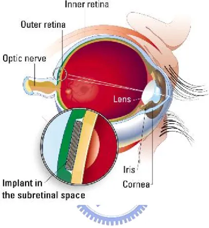
The fundamental concept of the Subretinal approach is that electrical charge generated by the microphotodiode array (MPA) in response to a light stimulus may be used to artificially alter the membrane potential of neurons in the remaining retinal layers in a manner to produce formed images [54]. The MPA functions in solar cell mode, that is, it operates without power supply. Fig. 1.4 shows the sub-retinal implant [55]. This approach would theoretically allow the remaining intact retinal circuits of the inner retina to process this signal in a near-normal fashion and transmit this signal to the brain. In addition, the sampling density of a subretinal device could be designed to match that of the remaining photoreceptor or bipolar cell matrix, thereby providing a potentially high-resolution input to the retina.
Although the current subretinal implants have less circuit complexity, they suffer from the problem that the pn junction diode in solar cell mode cannot differentiate the light intensity in a wide range. Due to the saturation of pn junction diode, the patient with subretinal implant may not differentiate the darkness and brightness. Therefore, it is important to improve the sensitiveness of light intensity of subretinal implants.
1.3 REVIEW ON POWER ISSUE IN ARTIFICIAL RETINAL PROSTHESIS
It is medically infeasible to have permanent wired connections pass through the eyeball wall because the wire would do quick damage to the eyes. Laying the wires and connecting the nodes entails extensive incisions, a potentially hazardous surgery. Therefore, the power issue is a great challenge for implanted retinal circuit.
Owing to lower stimulus level, sub-retinal chip usually consists of photodiode and electrode array which provides stimulus of low energy [54]. Thus sub-retinal chip requires no power supply. However, this kind of artificial retinal prosthesis can only replace the photoreceptor, a cell converting light into electrical signal. If more than the damage of photoreceptor causes blindness, the typical sub-retinal chip cannot restore the vision.
A common way to provide the implanted retinal circuit power is utilization of RF telemetry [2], [49]-[53]. This kind of implanted device consists of an extraocular and intraocular unit. The implantable component receiver power and a data signal via a telemetric inductive link between the two units. The extraocular unit includes a video camera and video processing board, a telemetry protocol encoder chip, and an RF amplifier and primary coil. The intraocular unit consists of a secondary coil, a rectifier
and regulator, a retinal chip with a telemetry protocol decoder, a stimulus signal generator, and an electrode array. The major difficulty for this telemetry technique is tissue heating associated with electromagnetic power deposition in the tissues and power dissipation in the microchip collectively.
The proposed method to supply power to implanted retinal chip is using solar cells. When the circuit is designed as low-power circuit, solar cells can provides enough energy to the implanted circuit. Two advantages of solar cell are described below. Firstly, when there is no light and therefore human cannot see, the solar cell supply no power to the implanted circuit. It clearly reduces some power dissipation and tissue heating. Secondly, solar cell is compatible with intraocular unit. Therefore, there is no equipments need to carry with the blind.
1.4 Motivations
The functions of photoreceptors, horizontal cells and bipolar cells are desired as a sub-retinal prosthesis. The method supply power to the implant chip is critical in the procedure of implantation. The power dissipation is necessary to avoid huge heat in the eyeball.
Fig. 1.1 The Human Eye. Reprinted from “Foundations of Physiological
Fig. 1.2 A Conceptual Epi-Retinal Prosthetic System. Reprinted form “A
Neuro-Stimulus Chip with Telemetry Unit for Retinal Prosthetic Device,” by Wentai Liu, and etc, 2000.
Fig. 1.3. The Typically Functional Implantable Epi-Retinal Microsystem. Reptinted
from “A Neuro-Stimulus Chip with Telemetry Unit for Retinal Prosthesis Device” by Wentai Liu, and etc., 2000.
Fig. 1.4. The Sub-Retinal Implant. Reprinted from the internet: “http://www.optobionics.com/theeye.htm” by Mike Zang.
CHAPTER 2
THE ARCHITECTURE OF VERTERATE RETINA
2.1 BACKGROUND
Vision contains abundant information. Therefore, animals devote a large fraction of their nervous system to vision. On the human cerebral cortex, about 55% of the nervous system is contributed to the computations underlying the perception of vision. Such a large computational system makes human easily perceive the surrounding world and control their actions. Vision is, therefore, one of the most important perception that human has.
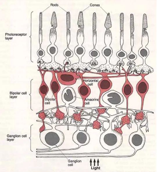
The retina is a complex structure, containing a variety of cell types with complex interconnections. According to the researches on biological retina, all vertebrate retinas are organized in the same basic plane where two synaptic layers called outer and inner plexiform layers are intercalated between three cellular layers called photoreceptor unclear layer, bipolar unclear layer, and ganglion cell layer. Fig. 2.1 shows the schematic diagram of the retinal circuitry of the vertebrate retinas. There are five basic classes of retinal neurons in the three cellular layers as shown in Fig. 2.1, namely, the photoreceptor, horizontal, bipolar, amacrine, and ganglion cells.
Light is transduced into electrical potential by the photoreceptors at the top. The primary signal pathway proceeds from the photoreceptors in the photoreceptor unclear layer through the synapse in the outer plexiform layer to the bipolar cells, and then to the retinal ganglion cells, the output cells of the retina. The horizontal cells are located just below the photoreceptors whereas the amacrine cells just below the ganglion cells. Both horizontal cells and amacrine cells spread across a large area of the retina to form layers transverse to the primary signal flow. The signals carried by the neurons in the retina can be divided into two types called graded potentials and action potentials. Graded potentials are observed in photoreceptor, horizontal, and bipolar cells whereas action potentials in amacrine and ganglion cells. Fig. 2.2 shows the intracellular response of typical recordings from a number of different cell types in the mudpuppy retina [56].
The properties of the five basic cells are described in the following subsections.
When light passes through the cornea, the pupil, the lens, the vitreous humor, and the transparent retina, it is finally captured by the most distal retina cells of the
photoreceptors, the input cells of the retina. The photoreceptor cells respond to the captured light only with the graded hyperpolarizing potentials as shown in the first row of Fig. 2.3. The potentials are used to activate the following neurons in the retina. All vertebrates so far examined appear to have at least two types of photoreceptors, which often can be classified as rod cells and cone cells. [57]. The human retina contains approximately 120 million rods and 6 million cones. Rods are more sensitive and used in moonlight. Cones are less sensitive and operated over a broad range of light intensities. Cones also convey color information.
2.3 THE HORIZONTAL CELLS
The responses of the horizontal cells are activated by the outputs of the photoreceptor-horizontal synapse in the outer plexiform layer. The horizontal cells respond to the inputs from the photoreceptor cells only with the graded hyperpolarizing potentials. There are large gap junctions existing among the horizontal cells. So when the current form the photoreceptor is injected through the synapse into horizontal cell, the injected current flows into the neighboring cells horizontally. This electrical coupling enables the horizontal cells to have a very large receptive field which is defined as the portion of the visual field to which a single neuron responds. The intracellular response of the horizontal cell from the mudpuppy retina are shown in the second row of Fig. 2.3.
At the layer of the horizontal cells, two functions are performed. Firstly, the clear image signals passed form the photoreceptors are slowed in times so that the outline blurs and rapid movements are transferred imperfectly. This is equivalent to transient low-pass filtering. Secondly, the spatial low-pass filtering takes place because the incoming excitation from each photoreceptor is spread into the adjacent region over this horizontal layer. Consequently, what the low-pass filtering of the horizontal layer does is to transform the photoreceptor output response into a function of average illumination in both time and space.
2.4 THE BIPOLAR CELLS
The responses of the bipolar cells are initiated by the outputs of both photoreceptor cells and horizontal cells through the synapses in the outer plexiform layer. The bipolar cells respond to the inputs from both photoreceptor cells and horizontal cells not only with graded hyperpolarizing potential but also with graded
depolarizing potentials.
According to the responses to the retinal illumination, there are two types of bipolar cells observed. The first type of cell is that hyperpolarizes in response to the illumination of the center of the cell’s receptive field. The second type of cell is that depolarizes in response to the center illumination. The former cells are called the hyperpolarizing or off-center bipolar cells whereas the later are called the depolarizing or on-center bipolar cells.
In the off-center bipolar cells, the photoreceptor-bipolar synapses are excitatory synapse whereas the horizontal-bipolar synapses are inhibitory synapse. Therefore, the off-center bipolar cells are hyperpolarized strongly in a graded and sustained fashion by the outputs of the photoreceptors cells whereas these bipolar cell potentials are antagonized by the outputs of the horizontal cells. Because the horizontal cells have a large receptive field and lateral extent in the outer plexiform layer than do the bipolar cells, a center-surround receptive organization is observed in the bipolar-cell response which is a center-surround receptive organization is observed in the bipolar-cell response which is a center-hyperpolarizing surround-depolarizing response. The intracellular responses of this type of cells from the mudpuppy retina are shown in the third row of Fig. 2.3. In the on-center bipolar cells, the photoreceptor-bipolar synapses are inhibitory synapses whereas the horizontal-bipolar synapses are excitatory synapses. The response of such bipolar cells is a center-depolarizing surround-hyperpolarizing response.
The off-center and on-center bipolar cells come in pairs in the retina. Therefore they can offer and add benefit: activity in paired populations falls on the opposite sides of a light-dark boundary, and thus signals a line edge. A line edge is nothing more than a boundary between light and dark.
2.5 THE AMACRINE CELLS
In most retinas, two basic types of amacrine cell responses, transient and sustained, have been observed. More is known about transient amacrine cells than the sustained ones. The transient amacrine cells usually give on- and off-responses to the illumination presented anywhere in their receptive fields and are also very responsive to moving stimuli. They always respond by depolarizing and are the first neurons along the visual pathway to respond primarily with transient and depolarizing potentials. The transient amacrine cells generally do no show a center-surround antagonistic receptive field organization. Action potentials are often seen superimposed o their depolarizing on- and off- responses. The fourth row of Fig. 2.3. shows the intracellular responses of the transient amacrine cell.
2.6 THE GANGLION CELLS
Most reports describe two basic kinds of ganglion cells which are the output cells of the retina: those that give sustained on-center or off-center responses and show an antagonistic surround and those that respond to flashes of light with transient on-off responses. The first type of cell is called the on-center ganglion cell or the off-center ganglion cell. The second type of cell is called the on-off ganglion cell. The responses of both two types of cells in the mudpuppy retina are shown in the last two rows of Fig. 2.3 where the responses of the sustained type are from an on-center ganglion cell. As shown in the fourth row of Fig. 2.3, the on-off ganglion cells give transient responses at the onset and cessation of stimulation, much as the transient amacrine cells do. These recordings show that the on-off ganglion cells would receive much, if not all, of their synaptic inputs from the transient amacrine cells. In addition to the transient responses at the onset and cessation of stimulation, the on-off ganglion cells respond very well to motion. Moreover, they may show direction-sensitive responses. According to the results of several experiments [58]-[59], these direction-sensitive responses are suggested to be mediated by two kinds of transient amacrine cells called excitatory and inhibitory amacrine cells.
Fig. 2.4 shows two schemes suggesting how direction-sensitive responses may be mediated by excitatory and inhibitory transient amacrine cells [60]-[61]. In the top scheme of Fig. 2.4, the inhibitory amacrine cell AI makes its synapses on the
excitatory amacrine cell AE. In the lower scheme of Fig. 2.4, the inhibitory amacrine
cell makes its junctions directly on the ganglion cell G dendrites. Movement of a spot of light in the preferred direction activates first the inhibitory amacrine cell, thus causes the inhibition of the excitatory amacrine cell (top scheme) or of the ganglion cell (bottom scehme) and the cancellation of excitatory input to the ganglion cell.
2.7 A SUMMARY OF FUNCTIONAL ORGANIZATION OF THE RETINA
Fig.2.5 summarizes much information and many ideas concerning the functional organization of the retina [62]. In summary, the outer plexiform layer of the retina responds mainly to both static and spatial aspects of illumination. The neurons in this layer consisting of the photoreceptors, the horizontal cells, and the bipolar cells, respond to stimuli primarily with sustained, graded potentials. The antagonistic center-surround organization at the level of the bipolar cells accentuates contrast in the retinal image. The on- and off-center ganglion cells, receiving much of their input directly from either center-depolarizing or center-hyperpolarizing bipolar cells, reflect
this basic center-surround receptive field organization established in the outer plexiform layer.
The inner plexiform layer, on the other hand, responds more to the dynamic or temporal aspects of photic stimuli. Both transient amacrine and on-off ganglion cells accentuate the changes in the retinal illumination and respond vigorously to moving stimuli. Interactions in the inner plexiform layer underlie the motion- and direction- sensitive responses of the on-off ganglion cells and the orientation-preferring response of some on- and off-center ganglion cells.
Fig. 2.1. The schematic diagram of the retinal circuitry of the vertebrate retinas.
Reprinted from “foundations of Physiological Psychology,” by Nwil R. Carlson, 1989, p. 136.
Fig. 2.2 Intracellular recording from the mudpuppy retina showing the difference in response of a given cell type to a 100-μm spot and to annuli of 0.5 and 1.0 mm in diameter, all at the same intensity. Reprinted from “ The Retina: An
Approachable Part of the Brain,” by J. E. Dowling, Cambridge, MA: Belknap Press of Harvard University Press, 1987, p. 84.
Fig. 2.3. Two schemes suggesting how direction-sensitive responses may be mediated by excitatory and inhibitory amacrine cells in the retina. In the top scheme, the inhibitory amacrine cell AI makes its synapses on the excitatory amacrine cell
AE processes. In the lower scheme, the inhibitory amacrine cell makes its
junctions directly on the ganglion cell G dendrites. (○: excitatory synapses; ●: inhibitory synapses; B: bipolar cell). Reprinted from “ The Retina: An
Approachable Part of the Brain,” by J. E. Dowling, Cambridge, MA: Belknap Press of Harvard University Press, 1987, p. 114.
Fig. 2.4. Summary scheme of the synaptic interactions that occur in the retina and that underlie the receptive field properties of the on-center, off-center, and on-off ganglion cells. (○: excitatory synapses; ●: inhibitory synapses; △: reciprocal synapses). Reprinted from “ The Retina: An Approachable Part of the Brain,”
by J. E. Dowling, Cambridge, MA: Belknap Press of Harvard University Press, 1987, p. 118.
CHAPTER 3
THE DESIGN, CHARACTERISTICS AND ANALYSIS OF ARTIFICIAL RETINA
3.1 THE CHARACTERISTICS OF PN JUNCTION DIODE AS ARTIFICIAL RETINA
In 1990, Dr. Gene de Juan and Dr. Mark Humayun first demonstrated that retinal ganglion cells could be electrically stimulated without penetrating the retinal surface [63]. Afterwards, bypassing the damaged retina with an artificial retina is the goal of many researchers around the world.
In certain diseases of the retina, the photoreceptor cells do not respond to light and thus causes blindness. If only the photoreceptor, light sensing part of retina, is damaged, the vision can be restored by replacing the photoreceptor only. The photoreceptor converts the light into electrical signal as the pn junction diode does. The absorption of light inside the diode creates electron-hole pairs, as pictured in Fig. 3.1 [64], where LP, LN and W are referred to as the minority carrier holes in an n-type
material, the minority carrier electrons in a p-type material and depletion width of pn diode respectively.
Minority carriers, holes in n-diffusion and electrons in p-diffusion, and carriers photogenerated within the depletion region are swept by the electric field to the opposite side of the junction, thereby contributing an added reverse-going component to the current through the diode. If the photogeneration rate (GL) is assumed to be
uniform through the diode, the added component due to light (IL) should be equal
to –g times the electron-hole pairs photogenerated per second in the volume A(LN+W+LP), or
I
I
I
L
dark
=
+
(3.1) withI
L= −
qA L
(
N+ +
W
L G
P)
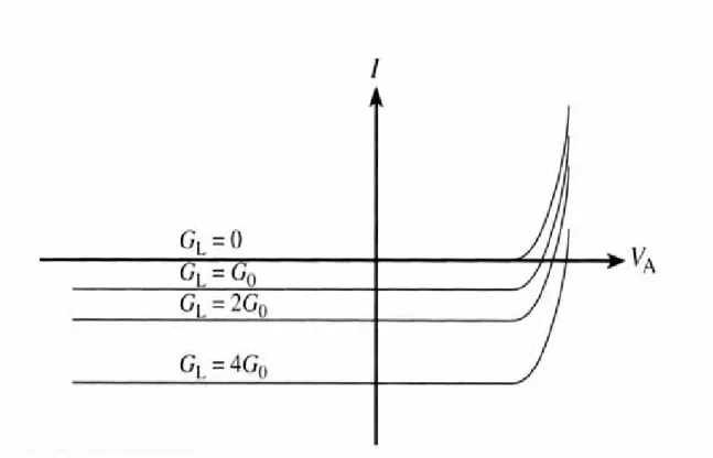
L (3.2) Examing Eq. (3.1), we note that the depletion width W of a pn junction diode in depletion region is typically small compared to LN+LP. If W is negligible, IL becomesindependent of the applied bias. The light-on I-V characteristics are therefore expected to be essentially identical to the dark I-V characteristics, except the light-on curves are translated downward, move in the –I direction, along the current axis. Moreover, because IL is proportional to GL, the downward translation of the
characteristics should increase in proportion to the intensity of the incident illumination. The described form of the photodiode I-V characteristics is illustrated in Fig. 3.2.
Due to the function of pn junction diode, transforming light into electrical signal, the pn junction diode in solar cell mode can be used as subretinal synthesis to replace photoreceptor in retina. There is, however, linearity problem, that is, the pn junction diode in solar cell mode cannot differentiate the light intensity in a wide range. Fig. 3.3 shows
According to the characteristics of pn junction diode, there are two different usages while applying pn junction diode to artificial retina. One is giving no bias, and the pn junction diode works as solar cell. The other is applying positive bias, and the pn junction diode function as CMOS image sensor. To differentiate the performance of theses two cases, two kinds of chips are designed and analyzed.
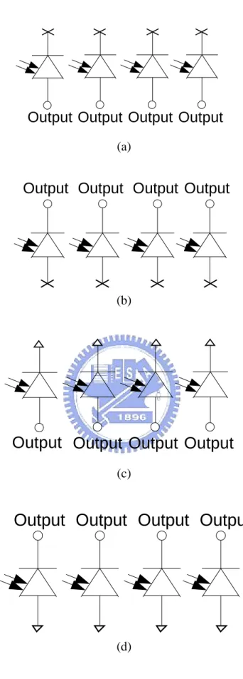
Firstly, a p+-n-well diode array is designed and fabricated. Because it is not clearly understood which kind of signal is transferred in mammalian retina, four different diode arrays are designed which are pictured in Fig. 3.3. Fig. 3.3 (a) shows a diode with n-type node floating and p-type node connected to an electrode to stimulate the cell while Fig. 3.3 (b) shows a diode with p-type node floating and p-type node connected to an electrode. When the light irradiates on the diode, the voltage across the two node of the diode would changes and thus a voltage signal stimulates the cell. Fig. 3.3 (c) and (d) picture a diode with one node connecting to ground and the other connect to an electrode to stimulate the cell. Because a closed loop is formed, the diode would send current of different magnitudes according to the light intensity.
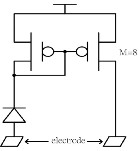
Secondly, the other utilization of p+-n-well diode is pictured in Fig. 3.4.One pixel contains a p+-n-well diode and a current mirror with current gain of 8 formed by PMOS. There are two electrodes in each pixel. The electrode connected to the pn diode provides the diode a close loop so that a photocurrent can be generated. The output current from the current mirror pass through the other electrode to stimulus the retinal cells. The current mirror serves as two functions. One is to bias the pn junction diode to ensure that the diode work at the third quadrant just as the CMOS sensor does. The other function is to amplify the photocurrent generated by the pn junction diode so that the area of pn junction diode can be made smaller. When the pn junction diode senses the light, a photocurrent is generated and amplified by a current mirror.
The pn junction diode operates in the third quadrant without doubt because n-type node connected to higher potential (closer to power supply). The amplified photocurrent stimulates the retinal cell through the electrode.
3.2 ANALYSIS OF THE PSEUDO-BJT-BASED SILICON RETINA
Although some patients can restore their vision by replacing photoreceptors, other patient may need replacing more retina cells, including bipolar cells and horizontal cells. Recall that the bipolar cell processes image edge detection function, and the horizontal cell process smoothing function.
The proposed silicon retina is based on Pseudo-BJT (PBJT) [65]. The PBJT is composed of two MOSFETs. Fig. 3.5 (a) shows the pseudo npn BJT. It possess two n-channel enhanced mode MOSFETs with the source and gate of MOSFEET M1 and the gate of MOSFET M2 connected at the same node, B. This structure is the same with the popular current-mirror arrangement. Therefore, the current gain approximately equals to the W/L ratio between the transistor M1 and M2. The input node B of the current mirror acts as the base of the PBJT. In the same way, the pseudo pnp BJT can be derived by two enhanced mode p-channel MOSFETs via similar arrangement as shown in Fig. 3.5 (b).
The photocurrent generated by pn junction diode is usually small, and therefore the PBJT work in the subthreshold region. The drain current in the subthreshold region can be expressed as [66]
[ ] /
(1
)
Vgs Vt VT Vds VT x dsW
I
K
e
e
L
η− −=
−
(3.3)where Vgs is the gate-to-source potential, Vds is the drain-to-source potential, VT=kT/q
is 26mV, Kx depends on process parameter, W/L is the geometric ratio of the MOS,η
is the subthreshold swing parameter [66]. Based on Eq. (3.3), the current gain of Pseudo-BJT can be written as
2 1 1 1 2 2 1 1 / ( )( ) 2 / 1
( ) [1
]
( ) [1
]
ds ds Vgs Vt T ds VT T ds V V W L W V V L I Ie
e
e
η ηβ
=
=
−
−− − −−
(3.4)Examining Eq. (3.4), the current gain beta is larger than desired value in low-induced current level due to the difference between Vds of master and slave
MOSFETs are close to each other. Thus the current gain beta approaches to the desired value. In order to reduce the affect of subthreshold swing parameter, the slave MOSFET must be structured by making parallel copies of the master MOSFET. Hence, the current gain beta would be independent on subthreshold swing parameter. A MOS resistor in subthreshold region is also used in the proposed silicon retina circuit. With the drain current in subthreshold region as shown in Eq. (3.3), the channel resistance RDS can be expressed as
[ ] ( ) 1
1
[
]
s V Vg V Vt ds VT VT x ds TW
R
K
e
e
V L
η− − − −=
(3.5)As shown in Eq. (3.5), the resistance can be adjusted by VG. The larger the gate voltage is, the smaller the channel resistance is.
In the PBJT-based silicon retina circuit shown in Fig. 3.6, a photo-PBJT, which consists of a photodiode D0 and an isolated PBJT, mimics the photoreceptor in a vertebrate. As indicated in chapter 2, the photoreceptor converts light into electrical signal, and pass it on to the horizontal cell and bipolar cell. The photodiode D0 generates the photocurrent which is amplified and passed on to the output node by the isolated PBJT. A smoothing PBJT and MOS resistors function as the horizontal cell. As indicated in chapter2, the horizontal cell spreads the incoming excitation form each photoreceptor into the adjacent region over this horizontal layer. The MOS resistors spread the photocurrent form the photodiode, while the smoothing PBJT amplifies the spread photocurrent and pass in on to the output node. The extracted current Iext is to substrate the current Iiso and Ismt, and thus the function of bipolar cell, edge extraction, is formed.
The edge-extracted function of this circuit can be explained as follows. When there is an edge, Iiso is larger than Ismt, and thus the current Iext is positive (direction from circuit to output) and the voltage at output node is low. When the pixel circuit does not locate at object edge, Iiso is smaller than Ismt, and thus Iext is negative and the voltage at output node is positive.
The architecture of 2-D retinal array is shown in Fig. 3.7. There are 32x4 pixels in the 2-D array. A column decoder is used to select the desired pixel. The column decoder, consist of invert and two-input and gate, converts five-bit binary column address to decimal number.
3.3 THE POWER SUPPLY ISSUE OF IMPLANTED SILICON RETINA
One significant challenge in implanted silicon retina is how to provide the implanted circuit power. The proposed method is to use pn junction diode as solar cell.
One advantage of solar cell as battery is that solar cell does not need to be replaced or charged. Therefore when the chip is implanted into the retina, oculists do not operate surgery once for a while due to the depletion of the battery energy.
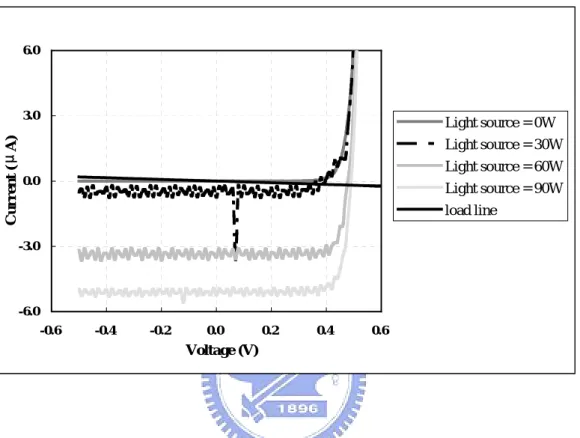
The determination of the area and the number of solar cells are described in the following. Firstly, the I-V characteristics of a teskey of pn junction diode under different input light source strength is measured and shown in Fig. 3.8. The testkey is a hundred of pn junction diode in parallel with area of 10μm x 10μm each. The detailed information about the testkey is shown in Table 4.1. From Fig. 3.8, it is obviously that the testkey shows the typical diode I-V characteristic. Note that pn junction diode is called solar cell when it operates in the fourth quadrant. Secondly, from HSPICE simulation, the power consumption of the circuit including total current and voltage is shown. With this information, a load line indicating the load of the power supply node can be drawn on the plane of the pn diode I-V characteristics. The intersection between the load line and the I-V curve of testkey shows the voltage and current that the testkey can provide for the circuit. Then from the voltage and current the circuit requires, the number of solar cells can be determined as several times of the testkey.
A true example of our Pseudo-BJT-based silicon retina circuit is shown below. The load line of the proposed circuit of eight pixels intersect the I-V curve under input light source of 60W at x=0.47 volt, y=-171nA as in Fig. 3.9. In HSPICE simulation, eight proposed pixel circuits require voltage supply being 0.7 volt and current supply being 233nA with photocurrent simulated in 1 nA. Thus the power supply demands 2 series-wound solar cells and 150 paralleled solar cells for eight pixel circuits. The total number of series-wound solar cell is 2, and the total number of parallel-wound solar cell is 1200 in implantable silicon retina array. However, if we need to measure the response of implantable silicon retina, the light intensity of image need to stronger than the light intensity illuminated on solar cells. Thus, the number of parallel-wound solar cell is over designed. Fig.3.10 shows the equivalent connection of one group of solar cells. The reference point utilizes the retina issue of potential being –60mV to 35mV. The same procedure can be applied to the design of the pn junction diode biased by current mirror.
3.4 SIMULATION RESULTS
3.4.1 Pseudo-BJT-Based Silicon Retina
pseudo-BJT. The HSPICE simulation bases on the device parameters of 0.35μm two-poly four-metal n-well CMOS technology. The designed current gain is 25 and the geometric ratio (W/L) is 0.4 μm over 0.35 μm for both NPN and PNP Pseduo-BJT. As indicated in section 3.2, in low-induced current level, the current gain is larger than designed value. When the induced current becomes larger, the current gain approaches to desired values as shown in Fig. 3.11.
Fig. 3.12 shows the smoothing function for the proposed Pseudo-BJT-based silicon retina shown in Fig. 3.6. A linear silicon retina array with 8 pixels being considered verifies the function of smoothing. The light is incident on the 3rd to the 6th pixels, while the photocurrent is simulated in two different current levels, that is1nA and 10nA. The simulated voltage of Vsmooth is –0.03 volt.
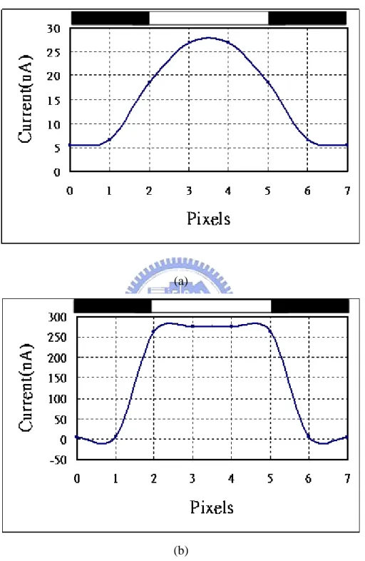
The edge-extract function for the proposed Pseudo-BJT-based silicon retina is shown in Fig. 3.13. The same condition as what in smoothing functions is considered. Note that the current peaks appear in the edge of the light image.
Fig. 3.14 shows the simulated output current waveform of a cell in a linear silicon retina array with the moving-object image incident on the array. The speed of the moving object is 1.25x 10⁶ cells/sec and the photocurrent is simulated in 1 nA. Fig. 3.15 (a) shows 2-dimensional pattern with the photocurrent incident on 16 pixels locating at the center of the chip of 64 pixels (8x8). The light window simulated in 1 nA is located at row 3rd to row 6th and column 3rd to column 6th. Fig. 3.15(b) shows the extracted output current under the situation described in Fig. 3.15 (a). Greater response occurs in four corners because the corners locate at the intersection of the two edges.
Fig. 3.16 shows the edge-extract function for the proposed Pseudo-BJT-based silicon retina. A linear silicon retina array with 32 pixels being considered verifies the function of edge-extraction. The light is incident on the 12th to the 19th pixels, while the photocurrent is simulated in two different current levels, that is 25nA and 125nA. The corresponding voltage of Vsmooth is 0.9volt and 1volt, respectively.
Fig. 3.17 shows the edge-extract function under different smoothing biases. A linear silicon retina array with 32 pixels is considered. The simulation condition is shows in Table 3.1.
Fig. 3.18 shows the flash reaction of the proposed silicon retina in a linear array with 32 pixels. The simulated condition is shown in Table 3.2. There is overshooting when the light turns on, but this phenomenon becomes unapparent when the input photocurrent decreases to 25nA.
Fig. 3.19 shows the effect of the capacitor produced by pn-diode in the pixel circuit. Fig.3.18 (a) shows the pre-simulation and post-simulation result of the flash reaction of the proposed silicon retina. The simulation condition is the same as Table
3.2.
Fig. 3.20 shows the parasitic N-well capacitor in the pixel circuit. The parasitic N-well capacitor is 345fF. Fig. 3.21 shows the comparison of simulation results with and without parasitic N-well capacitor.
Table 3.3 shows the power supply rejection ratio of the proposed silicon retina. The power supply rejection ration is defined as the ration of current gain of input and current gain of power supply. Consider Pseudo-BJT, the current gain of input current is 26.7 while the current gain of VDD and VSS power supply current is 0.105 and 0.405. Consider the output node, the current gain of input current is 8.8 while the current gain of VDD and VSS power supply is 0.1 and 0.41. Table 3.4 shows the simulated condition of the power supply rejection ratio in Table 3.3.
Fig. 3.22 shows the model to simulate the pn-diode which operates in solar cell mode. The current control current source F1 is used to generate the diode current. The current source Ip is used to generate photocurrent while the pn-diode is under illumination. The summation of the pn-diode current and photocurrent flows through the output resistor to define the bias condition of the pn-diode by a voltage control voltage source which. The components and their corresponding meaning are shown in Table 3.5.
With the solar cell model shown in Fig. 3.22, the simulated flash light reaction of solar cell is shown in Fig. 3.23. As the light turns on, the voltage of solar cell increases to a stable voltage in a very quick manner. As the light turns off, the voltage of the solar cell decreases slowly. Since the artificial retina need not work while the light is off, the unstable voltage of solar cell would not affect the performance the silicon retina. Thus, the solar cell is suitable power supply for silicon retina.
Fig. 3.1 Visualization of light absorption, electron-hole creation, and the light-induced current in a pn junction diode. Reprinted from “Semiconductor Device Fundamentals,” by Robert F. Pierret, 1996, pp. 349.
Fig. 3.2 Photodiode I-V characteristics. Reprinted from “Semiconductor Device Fundamentals,” by Robert F. Pierret, 1996, pp. 350.
Output Output Output Output
(a)
Output Output Output Output
(b)
Output Output Output Output
(c)Output Output Output Output
(d)
Fig. 3.4. A p+-n-well diode and a current mirror with current gain of 8 formed by PMOS as the artificial retina.
(a)
(b)
Fig. 3.5. The circuit diagram of (a) npn pseudo-BJT (PBJT) and its device symbol, (b) pnp pseudo-BJT (PBJT) and its device symbol.
Fig. 3.6. The pixel circuit of the proposed low-power implantable PBJT-based retina circuit.
Fig. 3.7 Architecture of 2-D retinal array of 32x4 pixels. The column decoder converts five-bit binary column address to decimal number.
CELL CELL CELL
CELL CELL CELL CELL Column Decoder Column Address
CELL CELL CELL CELL
CELL CELL
CELL
CELL
CELL CELL CELL CELL CELL
4
…………
……
-2.00E-05 -1.50E-05 -1.00E-05 -5.00E-06 0.00E+00 5.00E-06 1.00E-05
-6.00E-01 -4.00E-01 -2.00E-01 0.00E+00 2.00E-01 4.00E-01 6.00E-01
V(volt)
I(A)
Phi=0W Phi=30W Phi=60W Phi=90W Phi=120W-6.0 -3.0 0.0 3.0 6.0 -0.6 -0.4 -0.2 0.0 0.2 0.4 0.6 Voltage (V) Current ( μA) Light source = 0W Light source = 30W Light source = 60W Light source = 90W load line
Fig. 3.9. Characteristic I-V curves of the teskey and a load line of the proposed circuits.
Fig, 3.10. One block of solar cell as power supply. Positive and negative power supply formed by 2 series-wound solar cells and 1200 paralleled solar cells respectively exploiting the tissue potential varying from -60mV to -35mV.
Fig. 3.11. The beta value (current gain) of the NPN pseudo-BJT (the upper one) and PNP pseudo-BJT (the lower one).
(a)
(b)
Fig. 3.12. The smoothing function of pseudo-BJT-based silicon retina simulated under the photocurrent of (a) 1nA, (b) 10nA.
(a)
(b)
Fig. 3.13. The edge-extract function of pseudo-BJT-based silicon retina simulated under the photocurrent of (a) 1nA, (b) 10nA.
Fig. 3.14. The simulated output current waveform of a cell in a linear silicon retina array with the moving-object image incident on the array. The generated photocurrent I is 1nA and the speed of the moving object is 1.25x 10⁶ cells/sec.
(a)
(b)
Fig. 3.15. (a) The 2-dimensional pattern with the photocurrent incident on 16 pixels locating at the center of the chip of 64 pixels (8x8). The light window simulated in 1 nA is located at row 3rd to row 6th and column 3rd to column 6th. (b) The corresponding edge-extract output current.
(a)
(b)
Fig. 3.16. (a) The edge-extract function for the proposed Pseudo-BJT-based silicon retina (32 pixels). The light is incident on the 12th to the 19th pixels, while the photocurrent is simulated in two different current levels, that is, 25nA (a) and 125nA (b). The corresponding voltage of Vsmooth is 0.9volt and 1volt, respectively.
Fig. 3.17. (a) The edge-extract function under different smoothing biases. A linear silicon retina array with 32 pixels is considered. The simulation condition is shows in Table 3.1.
Fig. 3.18.The flash reaction of the proposed silicon retina in a linear array with 32 pixels. There is overshooting when the light turns on, but this phenomenon becomes unapparent when the input photocurrent decreases to 25nA.
Fig. 3.19. The pre-simulation and post-simulation result of the flash reaction of the proposed silicon retina. The simulation condition is the same as Table 3.2.
Fig. 3.20. The parasitic N-well capacitor in the pixel circuit. The parasitic N-well capacitor is 345fF. to up cell to left cell to down cell to right cell Smooth D0 Isolated PBJT Smoothing PBJT VDD VSS Iiso Ismt Iext M1 M2 M3 M4 M5 M6 M8 M7 NW Cap
(a)
(b)
Fig. 3.21 The comparison of simulation results with (a), and without parasitic N-well capacitor (b).
Table. 3.3 The power supply rejection ratio of the proposed silicon retina.
Fig. 3.22. The model to simulate the pn-diode which operates in solar cell mode.
diode
D0
current source
I1
current control current
source
F1
voltage control voltage
source
E1
diode
D0
current source
I1
current control current
source
F1
voltage control voltage
source
E1
CHAPTER 4
EXPERIMENTAL RESULTS
4.1 LAYOUT DISCREPTION
Two experimental chips are designed and fabricated in a 0.35um double-poly-four-level-metal N-well CMOS technology for implantation and instrument measurement respectively. The chip for implantation consists of a 8x8 array of the proposed Pseudo-BJT-based silicon retina circuit. The total solar cells of area 1064064um2 divided into four blocks. Each blocks contains 2 series-wound and 1200 parallel-wound solar cells. Each pixel occupies area of 900 um2 while the photodiode in each occupy 300um2. Fig 4.1(a), (b) and (c) shows the photograph of the basic cell in the 2-D array, photodiode in single pixel and solar cells respectively whereas Fig. 4.1(d) shows the photograph of the whole implantation chip. The chip for instrument measurement consists of 4x32 array of the proposed Pseudo-BJT-based silicon retina circuit, a decoder and solar cells of area 1097600um2. Figure 4.2 (a) and (b) shows the photograph of the whole chip and the decoder respectively. The ratio between total pixel area and total solar cell area is 10.5%.
4.2 MEASUREMENT RESULTS
Fig. 4.3 (a) shows the measurement setup chart where as Fig. 4.3 (b) shows the corss-sectional drawing of the setup for the chip. The light source is white light provided by illuminator, DRILE model 66182 and model 68830, while the convex with focus of 28cm focuses the light on the chip. The measurement is done with Hp 4145B semiconductor parameter analyzer which biases the output node at half dc power supply. The opaque material is used to shield the light to form the boundary of the light and dark. Figure. 4.4 (a) and (b) shows power and the luminance of the light on the chip versus different input light power under this setup condition. Table 4.1 shows the corresponding luminance of the input light power.
Fig. 4.5 (a) shows the I-V characteristics of the solar cell in the chip for instrument measurement under different luminance. Fig. 4.6 (a) and (b) shows the open circuit voltage and short circuit current. From Fig. 4.6, one can know that the photocurrent generated by solar cell increase dramatically while the light intensity