1010 IEEE ELECTRON DEVICE LETTERS, VOL. 28, NO. 11, NOVEMBER 2007
High-Performance Short-Channel Double-Gate
Low-Temperature Polysilicon Thin-Film Transistors
Using Excimer Laser Crystallization
Chun-Chien Tsai, Kai-Fang Wei, Yao-Jen Lee, Hsu-Hsin Chen,
Jyh-Liang Wang, I-Che Lee, and Huang-Chung Cheng
Abstract—In this letter, high-performance low-temperature polysilicon thin-film transistors (TFTs) with double-gate (DG) structure and controlled lateral grain growth have been demon-strated by excimer laser crystallization. Via a proper excimer laser condition, along with the a-Si step height beside the bottom gate, a superlateral growth of Si was formed in the channel length plateau. Therefore, the DG TFTs with lateral silicon grains in the channel regions exhibited better current–voltage characteristics, as compared with the conventional top-gate ones. The proposed DG TFTs (W/L = 1/1 µm) had the field-effect mobility exceed-ing 550 cm2/V· s, an
ON/OFFcurrent ratio that is higher than 108, superior short-channel characteristics, and higher current drivability. In addition, the device-to-device uniformity could be improved since grain growth could be artificially controlled by the spatial plateau structure.
Index Terms—Double gate (DG), excimer laser crystallization (ELC), lateral grain growth, thin-film transistor (TFT).
I. INTRODUCTION
A
DOUBLE-GATE (DG) structure is expected to be the alternative device structure for the ultimate high-performance ideal MOSFETs. These devices possess the potential advantages of excellent control of short-channel effects (SCEs) and drain-induced barrier lowering (DIBL), larger ON/OFFcurrent ratio, and higher channel conductivity [1]–[7]. If this advanced structure is applied to polycrystalline-Si (poly-polycrystalline-Si) and amorphous-polycrystalline-Si (a-polycrystalline-Si) thin-film transistors (TFTs), the performance of TFTs will also be improved. Poly-Si TFTs suffer from worse electrical characteristics, however, than bulk Si MOSFETs, owing to the presence of numerous intragrain and intergrain defects in the polysilicon films. There-fore, a variety of a-Si crystallization techniques have been proposed to produce low-temperature polysilicon (LTPS) TFTsManuscript received August 9, 2007. This work was supported in part by the National Science Council of Taiwan under Contract NSC 95-2221-E-009-252, and the Chunghwa Picture Tubes and in part by the Nano Facility Center of National Chiao Tung University and National Nano Device Laboratories (NDL) for providing process equipment. The review of the letter was arranged by Editor J. Sin.
C.-C. Tsai, K.-F. Wei, H.-H. Chen, J.-L. Wang, I-C. Lee, and H.-C. Cheng are with the Department of Electronics Engineering and Institute of Electronics, National Chiao Tung University, Hsinchu 30010, Taiwan, R.O.C. (e-mail: [email protected]).
Y.-J. Lee is with NDL, Hsinchu 30078, Taiwan, R.O.C.
Color versions of one or more of the figures in this letter are available online at http://ieeexplore.ieee.org.
Digital Object Identifier 10.1109/LED.2007.908473
with silicon-on-insulator-like performance [8]–[10]. Excimer laser crystallization (ELC) seems to be the most promising method at the moment for its great potential in mass production and high-quality silicon grains without damage to glass sub-strates. Although large grains can be attained in the superlateral growth (SLG) regime by ELC, many fine grains still spread between these large grains due to the narrow process window for producing large-grain poly-Si [11], [12]. Consequently, nonuniform and randomly distributed poly-Si grains will result in large variation of TFT performance when the laser energy density is controlled in the SLG regime, particularly, for small-dimension TFTs [13], [14]. Thus, many laser crystallization methods have been proposed to produce large grains with uniform grain size distribution, including sequential lateral solidification [15], the grain filters method [16], capping the re-flective or antirere-flective layer [17], phase-modulated ELC [18], dual-beam excimer laser annealing (ELA) [19], double-pulsed laser annealing [20], selectively floating a-Si active layer [21], continuous-wave laser lateral crystallization [22], selectively enlarging laser crystallization [23], and so on. However, some of them are not readily attached to existing ELA systems or are problematic for circuit layout due to the anisotropy of the grain boundary spacing.
In this letter, high-performance DG LTPS TFTs with a simple ELC method have been demonstrated. Because of the DG operation mode and lateral silicon grains formed in the channel region, the devices have a high driving current, steeper subthreshold slope, superior SCE immunity, and suppression of the floating-body effect. Moreover, not only are the fabrication process steps highly compatible with the conventional commer-cial a-Si TFTs but the uniformity of device performance can also be further improved.
II. DEVICEFABRICATION
Fig. 1 displays the key fabrication steps for the proposed DG short-channel LTPS TFTs structure crystallized with ELA. At first, a 1000-Å-thick phosphorus-doped polysilicon layer was deposited by low-pressure chemical vapor deposition (LPCVD) at 550◦C on silicon wafer with an oxide thickness of 1 µm. After defining the bottom-gate region, a 1000-Å-thick tetraethyl orthosilicate (TEOS) bottom-gate oxide layer was deposited by plasma-enhanced chemical vapor deposition (PECVD) at
TSAI et al.: HIGH-PERFORMANCE SHORT-CHANNEL DG LTPS TFTs USING ELC 1011
Fig. 1. Key process procedures for fabricating the proposed short-channel DG LTPS TFTs with lateral silicon grains.
385◦C, following a 1000-Å-thick a-Si layer that was deposited by LPCVD at 550◦C. Then, the samples were performed by a semi-Gaussian-shaped KrF ELC (λ = 248 nm) in a vacuum chamber pumped down to 10−3torr at room temperature. The number of laser shots per area was 20 (i.e., 95% overlap-ping), and the laser energy density was varied. After laser crystallization, the poly-Si active layers were etched to define the active channel region, and a 1000-Å-thick TEOS top-gate (TG) oxide was subsequently deposited. The poly-Si layer was deposited by LPCVD for the formation of the TG electrode. Then, the poly-Si thin films were etched by reactive ion etching to form TG electrodes, and a phosphorous ion implantation with a dose of 5× 1015 cm−2 was carried out to form source and drain regions. Next, a TEOS passivation oxide layer was deposited by PECVD, and the implanted dopants were activated by thermal annealing at 600◦C for 12 h. Contact hole opening and metallization were carried out to complete the fabrication of DG TFTs. Then, a 30-min sintering process was performed at 400 ◦C to reduce the contact series resistance of the source and drain electrodes. Finally, LTPS TFTs were passivated by a 2-h NH3 plasma treatment to further improve the device performance. For comparison, the conventional ELC TG LTPS TFTs with a channel thickness of 1000 Å were also fabricated using the SLG laser annealing condition in the same run.
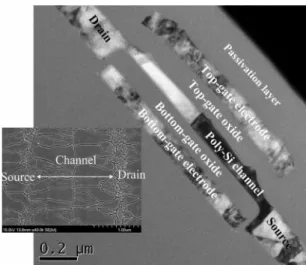
Fig. 2. Focus-ion-beam-prepared cross-sectional TEM photograph of excimer-laser-crystallized DG LTPS TFT with a gate length of 1.2 µm. The inset of Fig. 2 is the plane-view SEM image of excimer-laser-crystallized poly-Si thin films.
III. RESULT ANDDISCUSSION
Fig. 2 displays the cross-sectional transmission electron mi-croscopy (TEM) photograph to analyze the microstructure of excimer-laser-crystallized poly-Si films and the gate-stacked structure of DG TFT with a gate length of 1.2 µm. It is observed that a spatially controlled silicon grain with a length of 0.60 µm formed in the channel region via the SLG phenomenon using excimer laser irradiation with the plateau structure, as shown in the insetted plane-view scanning electron microscopy (SEM) image of Fig. 2. Moreover, the originally thicker a-Si films around the edges of the step height caused by the bottom gate become thinner and smoother. This phenomenon is attributed to two mechanisms, which are the reflow of molten silicon into the sunken regions during ELA and the capillary waves that were excited by the volume change at the silicon melt transition [24]. This thinner poly film around the edges of the step height may exhibit larger series resistance, which in turn reduces the driving current of the DG TFT. Fig. 3 shows the typical transfer and output characteristics of DG LTPS TFTs and conventional TG ones for W = L = 1 µm. Owing to the uniformly large transverse grains grown in the device channel region and DG operation mode, these proposed DG TFTs exhibit better electrical characteristics than the TG ones. The threshold voltage was defined as the gate voltage that is required to achieve a normalized drain–current of Ids= (W/L)× 10−8A at Vds= 0.1 V. The field-effect mobility and subthreshold swing (SS) were extracted at Vds= 0.1 V, and the
Ion/Ioff current ratio was defined at Vds= 3 V. The nominal mobility of the DG TFT was calculated from gm, which we
defined as a TG TFT of the same gate length and gate width with a 100-nm gate-SiO2layer. Obvious improvement in device characteristics is obtained for DG TFTs, instead of TG TFTs: The threshold voltage decreases from −1.60 to −1.55 V, SS decreases from 0.258 to 0.172 V/dec, the field-effect mobility increases from 186 to 550 cm2/V· s, Ion/Ioff increases from 4.37× 10⁷ to 4.35× 10⁸, and DIBL decreases from 0.241 to 0.075. In order to avoid the threshold voltage difference, the
1012 IEEE ELECTRON DEVICE LETTERS, VOL. 28, NO. 11, NOVEMBER 2007
Fig. 3. Current–voltage curves of DG TFT and the conventional TG one. (a) Transfer characteristics. (b) Output characteristics.
applied gate driving voltages in Fig. 3(b) are kept at constant values of|Vg− Vth|. It is demonstrated that poly-Si TFTs with location-controlled silicon grain structure and DG operation mode provide higher driving current than conventional TG TFTs under the same bias condition. The superior short-channel characteristics and driving capability imply that the proposed DG TFT is more suitable for scaled-down device applications.
The grain boundary trap state densities N t of the conven-tional TG and proposed DG poly-Si TFTs are estimated accord-ing to the Levinsons analysis [25], [26]. N t is extracted from the slopes of ln(ID/VGS) versus 1/(VGS) at VDS = 0.1 V and
high VGS. It can be found that a DG poly-Si TFT exhibits an N t of 2.35× 1011cm−2, which is two times smaller than that of the conventional TG one. This result implies that DG TFTs with lateral silicon grains possess better crystallinity and fewer microstructure defects, which are also confirmed by the cross-sectional TEM image shown in Fig. 2.
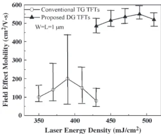
Fig. 4 displays the dependence of field-effect mobility on laser energy densities for DG TFTs and conventional ones, whose channel length is 1 µm. Twenty TFTs were measured for each laser irradiation condition to investigate the device-to-device uniformity. Compared with the conventional TG-TFTs,
Fig. 4. Dependence of field-effect mobility on applied laser energy density for DG TFTs with lateral silicon grains and conventional TG ones.
it was found that DG TFTs with lateral silicon grains exhibited smaller electrical deviation since the similar grain structures were formed when the applied laser energy densities were be-tween the threshold value of completely melting 1000-Å-thick silicon films in the channel region and that of partially melting thicker ones near the edges of bottom-gate electrode. Therefore, a broadened process window and improved uniformity of the TFTs’ performance are attained due to artificially lateral grains.
IV. CONCLUSION
Novel high-performance DG LTPS TFTs have been fabri-cated by ELC. Such TFTs exhibit a high field-effect mobility of 550 cm2/V· s and excellent short-channel characteristics because of the large transverse grains artificially grown in the channel region and DG structure for better gate controllability. In addition, the experimental results reveal a steeper subthresh-old value, higher driving current, suppressed kink current, and excellent device uniformity in proposed TFTs. The DG TFTs are therefore ideally suitable for future active-matrix organic light-emitting diode and 3-D integrated circuit applications.
REFERENCES
[1] J. M. Hergenrother, D. Monroe, F. P. Klemens, A. Kornblit, G. R. Weber, W. M. Mansfield, M. R. Baker, F. H. Baumann, K. J. Bolan, J. E. Bower, N. A. Ciampa, R. A. Cirelli, J. I. Colonell, D. J. Eaglesham, J. Frackoviak, H. J. Gossmann, M. L. Green, S. J. Hillenius, C. A. King, R. N. Kleiman, W. Y.-C. Lai, J. T.-C. Lee, R. C. Liu, H. L. Maynard, M. D. Morris, S. H. Oh, C. S. Pai, C. S. Rafferty, J. M. Rosamilia, T. W. Sorsch, and H. H. Vuong, “The vertical replacement-gate (VRG) MOSFET: A 50-nm vertical MOSFET with lithography-independent gate length,” in IEDM
Tech. Dig., 1999, pp. 75–78.
[2] S. Venkatesan, G. W. Neudeck, and R. F. Pierret, “Dual-gate operation and volume inversion in n-channel SOI MOSFET’s,” IEEE Electron Device
Lett., vol. 13, no. 1, pp. 44–46, Jan. 1992.
[3] H. S. P. Wong, K. K. Chan, and Y. Taur, “Self-aligned (top and bottom) double-gate MOSFET with a 25 nm thick silicon channel,” in IEDM Tech.
Dig., 1997, pp. 427–430.
[4] J. P. Colinge, M. H. Gao, A. Romano-Rodriguez, H. Maes, and C. Claeys, “Silicon-on-insulator “gate-all-around device”,” in IEDM Tech.
Dig., 1990, pp. 595–598.
[5] T. Tanaka, H. Horie, S. Ando, and S. Hijiya, “Analysis of p+ poly Si double-gate thin-film SOI MOSFETs,” in IEDM Tech. Dig., 1991, pp. 683–686.
TSAI et al.: HIGH-PERFORMANCE SHORT-CHANNEL DG LTPS TFTs USING ELC 1013
[6] D. Hisamoto, W. C. Lee, J. Kedzierski, E. Anderson, H. Takeuchi, K. Asano, T. J. King, J. Bokor, and C. Hu, “A folded-channel MOSFET for deep-sub-tenth micron era,” in IEDM Tech. Dig., 1998, pp. 1032–1034. [7] C. H. Wann, R. Tu, B. Yu, and C. Hu, “A comparative study of advanced
MOSFET structures,” in VLSI Symp. Tech. Dig., 1996, pp. 32–33. [8] Y. Helen, R. Dassow, M. Nerding, K. Mourgues, F. Raoult, J. R. Kohler,
T. Mohammed-Brahim, R. Rogel, O. Bonnaud, J. H. Werner, and H. P. Strunk, “High mobility thin film transistors by Nd:YVO4-laser crystal-lization,” Thin Solid Films, vol. 383, no. 1/2, pp. 143–146, Feb. 2001. [9] Z. Meng, M. Wang, and M. Wong, “High performance low
tempera-ture metal-induced unilaterally crystallized polycrystalline silicon thin film transistors for system-on-panel applications,” IEEE Trans. Electron
Devices, vol. 47, no. 2, pp. 404–409, Feb. 2000.
[10] C. W. Lin, L. J. Cheng, Y. L. Lu, Y. S. Lee, and H. C. Cheng, “High performance low-temperature poly-Si TFTs crystallized by excimer laser irradiation with recessed-channel structure,” IEEE Electron Device Lett., vol. 22, no. 6, pp. 269–271, Jun. 2001.
[11] J. S. Im, H. J. Kim, and M. O. Thompson, “Phase transformation mech-anisms involved on excimer laser crystallization of amorphous silicon films,” Appl. Phys. Lett., vol. 63, no. 14, pp. 1969–1971, Oct. 1993. [12] J. S. Im and H. J. Kim, “On the super lateral growth phenomenon observed
in excimer laser-induced crystallization of thin Si films,” Appl. Phys. Lett., vol. 64, no. 17, pp. 2303–2305, Apr. 1994.
[13] K. Yamaguchi, “Modeling and characterization of polycrystalline-silicon thin-film transistors with a channel-length comparable to a grain size,”
J. Appl. Phys., vol. 89, no. 1, pp. 590–595, Jan. 2001.
[14] M. Kimura, S. Inoue, T. Shimoda, and T. Eguchi, “Dependence of polycrystalline silicon thin-film transistor characteristics on the grain-boundary location,” J. Appl. Phys., vol. 89, no. 1, pp. 596–600, Jan. 2001. [15] R. S. Sposili and J. S. Im, “Sequential lateral solidification of thin sili-con films on SiO2,” Appl. Phys. Lett., vol. 69, no. 19, pp. 2864–2866,
Nov. 1996.
[16] P. C. van der Wilt, B. D. van Dijk, G. J. Bertens, R. Ishihara, and C. I. M. Beenakker, “Formation of location-controlled crystalline islands using substrate-embedded seeds in excimer-laser crystallization of silicon films,” Appl. Phys. Lett., vol. 79, no. 12, pp. 1819–1821, Sep. 2001.
[17] L. Mariucci, R. Carluccio, A. Pecora, V. Foglietti, G. Fortunato, P. Legagneux, D. Pribat, D. Della Sala, and J. Stoemenos, “Lateral growth control in excimer laser crystallized polysilicon,” Thin Solid
Films, vol. 337, no. 1/2, pp. 137–142, Jan. 1999.
[18] C. H. Oh, M. Ozawa, and M. Matsumura, “A novel phase-modulated excimer-laser crystallization method of silicon thin films,” Jpn. J. Appl.
Phys. 2,Lett., vol. 37, no. 5A, pp. L492–L495, May 1998.
[19] R. Ishihara, A. Burtsev, and P. F. A. Alkemade, “Location-control of large Si grains by dual-beam excimer-laser and thick oxide portion,” Jpn. J.
Appl. Phys. 1,Regul. Rap. Short Notes, vol. 39, no. 7A, pp. 3873–3878,
Jul. 2000.
[20] K. Yamazaki, T. Kudo, K. Seike, D. Ichishima, and C. G. Jin, “Double-pulsed laser annealing system and polycrystallization with green DPSS laser,” in Proc. AMLCD Tech. Dig., 2002, pp. 149–152.
[21] C. H. Kim, I. H. Song, W. J. Nam, and M. K. Han, “A poly-Si TFT fabricated by excimer laser recrystallization on floating active structure,”
IEEE Electron Device Lett., vol. 23, no. 6, pp. 315–317, Jun. 2002.
[22] A. Hara, M. Takei, F. Takeuchi, K. Suga, K. Yoshino, M. Chida, T. Kakehi, Y. Ebiko, Y. Sano, and N. Sasaki, “High performance low temperature polycrystalline silicon thin film transistors on non-alkaline glass produced using diode pumped solid state continuous wave laser lateral crystalliza-tion,” Jpn. J. Appl. Phys. 1,Regul. Rap. Short Notes, vol. 43, no. 4A, pp. 1269–1276, 2004.
[23] M. Tai, M. Hatano, S. Yamaguchi, T. Noda, S. K. Park, T. Shiba, and M. Ohkura, “Performance of poly-Si TFTs fabricated by SELAX,” IEEE
Trans. Electron Devices, vol. 51, no. 6, pp. 934–939, Jun. 2004.
[24] D. K. Fork, G. B. Anderson, J. B. Boyce, R. I. Johnson, and P. Mei, “Capillary waves in pulsed excimer laser crystallized amorphous silicon,”
Appl. Phys. Lett., vol. 68, no. 15, pp. 2138–2140, Apr. 1996.
[25] L. Levinson, F. R. Shepherd, P. J. Scanlon, W. D. Westwood, G. Este, and M. Rider, “Conductivity behavior in polycrystalline semiconductor thin film transistors,” J. Appl. Phys., vol. 53, no. 2, pp. 1193–1202, Feb. 1982.
[26] R. E. Proano, R. S. Misage, and D. G. Ast, “Development and electrical properties of undoped polycrystalline silicon thin-film transistors,” IEEE