國
立
交
通
大
學
電子工程學系 電子研究所
博 士 論 文
藉由離子佈植進入矽合金法在
低溫活化下形成的接面研究
A Study of Low Temperature Activated Junction Formed by
Implant Into Silicide Method
研 究 生:林建宏
指導教授:張國明 教授
藉由離子佈植進入矽合金法在
低溫活化下形成的接面研究
A Study of Low Temperature Activated Junction Formed by
Implant Into Silicide Method
研 究 生:林建宏 Student:Jian-Hong Lin
指導教授:張國明 Advisor:Kow-Ming Chang
國 立 交 通 大 學
電子工程學系 電子研究所
博 士 論 文
A DissertationSubmitted to Department of Electronics Engineering And Institute of Electronics
College of Electrical and Computer Engineering National Chiao Tung University
In Partial Fulfillment of the Requirements For the Degree of Doctor of Philosophy
In
Electronics Engineering
July 2008
Hsinchu, Taiwan, Republic of China
藉由離子佈植進入矽合金法
在低溫活化下形成的接面研究
學生:林建宏
指導教授:張國明 博士
國 立 交 通 大 學
電子工程學系 電子研究所博士班
中文摘要
隨著元件尺寸的微縮,為了確保元件的良好表現,有許多新的材料被導入元件 的製程。然而這些新材料的熱穩定性並不十分一致,導致製程整合的複雜化。有 些在其他特性表現不錯的材料也因此不被採用。究其原因,離子植入後的高溫活 化是製程整合上的主要瓶頸。離子佈植進入矽合金法是一種能在低溫下活化載子 的方法。本篇研究主要著重利用離子佈植進入鎳矽合金法在低溫活化形成的接面 特性的相關研究。 第一部分,我們想研究低溫活化的可能機制。首先我們藉由製作金屬半導體 二極體的測試結構,量測在不同的活化條件下,載子活化的情形,確認了低溫活 化下,在金屬和半導體接面的載子具有相當高的活化程度。藉由此部分的研究成 果,讓我們可以接著去設計實驗來觀察並且分析利用此離子佈植入鎳矽合金法在 低溫活化形成的 PN 接面。接著,我們分析了深淺兩種不同的佈植深度所形成的接 面行為的變化差異,提出了三個離子佈植入鎳矽合金法的在低溫活下可能的活化 機制,包含了金屬促發的再結晶,固態長晶再結晶,以及基材本身活化。 第二部分,我們想對藉由離子佈植入鎳矽合金法形成之接面特性做進一步的 了解。首先,根據第一部分的研究結果,為了研究 very shallow junction,我們 降低了植入載子的濃度,觀察並且記錄了相關的電特性且與先前的高離子佈植的 元件比較。接著,導入了第三段的熱製程溫度,觀察了元件的熱穩定度特性。藉 由交叉比對實驗結果,我們對於該元件的製作和量測方法提出了我們的觀點。A Study of Low Temperature Activated Junction Formed by
Implant Into Silicide Method
Student:
Jian-Hong
Lin
Advisor:
Dr.
Kow-Ming
Chang
Department of Electronics Engineering and
Institution of Electronics
National Chiao Tung University
Abstract
Many new materials have been introduced to ensure the device with high quality as
their physical lengths are scaled down. However, some materials may not have good
thermal reliabilities, hence making the process integration more and more complex. As
the result, some materials may have good characteristics in many aspects, but they
couldn’t be adapted to the fabrication process. The highest temperature appears in
device fabrication is the dopant activation step after implantation and this step
dominates the thermal reliability requirement for all materials. Implant into silicide
method is one possible method to activate dopant at low temperature. And in this study,
we focus on the characteristics of junction formed at low activation temperature by
using implant into nickel silicide method.
temperature. At first, we fabricated Metal Semiconductor diode (MS diode) test
structure at different activation conditions. By measuring and analyzing the dopant
activation abilities of MS diodes formed at different conditions, we confirm the factor
that even at low temperature activation, the dopant at the MS interface also has high
activation ability. Based on this result, we can go a step further to design an experiment
to observe and analyze behaviors of junction formed by the implant into nickel silicide
method. Then, by comparing different behaviors of junctions (deeper and shallow) with
two implantation energies, we proposed three possible corresponding dopant activation
mechanisms at low temperature to the implant into nickel silicide method. Which
includes doping activation at metal assisted re-crystallization region, solid phase
regrowth region and bulk activation region. In part II, we want to understand
characteristics of the junction formed by IIS method further. By the experimental results
in Part I, for very shallow junction fabrication, we lowered the implantation dosages and
then we record relative electrical properties and also compare results to the heavily
implanted samples. Then, an added thermal treatment is adapted to explore the thermal
reliability issue of these devices. By cross comparing experimental results, we proposed
our viewpoints of the IIS method.
誌 謝 (Acknowledgement)
寒夜客來茶當酒 風雨飄搖故人情 算算在交大的日子,連同碩士班一起,也過了六年。六年來的點滴,也讓我 在固態電子的領域,從一片荒蕪,也慢慢的長出了一片綠地。首先,要感謝指導 教授張國明老師的提攜,沒有老師的接受和鼓勵,我是不可能進入到這個領域。 在我進入碩士班後,謝謝許鉦宗老師,游凱翔博士的幫忙,讓我的研究視野,能 有進一步的拓展。上了博士班以後,張老師也總在後面默默的付出指導,幫忙的 找資源,提供可以思考的方向,但從來不阻止學生的研究興趣。不怕學生犯錯, 鼓勵學生從荊棘叢中走出一條屬於自己的道路。謝謝老師的教誨。 上了博士班後,尋找屬於自己能發揮的一小塊立足點,謝謝孫成業、楊志祥、 林勝軍、林詩帆和張庭嘉幾位學弟,一同在實驗上的幫忙,讓我的論文和實驗可 以順利的進行和完成。學弟,謝謝你們。 當我由學弟的角色,逐漸的變成博士班高年級的學長,也開始常常會聽到實 驗室不同研究領域的學弟,問起各式不同的問題。除了拓展了我的視野外,幾年 下來,面對不同研究的問題,只能在基本的原理原則下,嘗試的去解構不同情境 下的問題的成因,再架構出比較可能比較可行的方向。在不斷的重新解構和架構 下,抓重點的能力慢慢的也被培養了起來,古人說的教學相長,真的是很有道理。 這也是我們實驗室博士班訓練中很有特色,我也很喜歡的一個地方。那些在我被 自己研究數據和實驗忙的焦頭爛額下還敢來問我問題的學弟們,也謝謝你們。 相逢即是有緣,所有實驗室的成員讓我這六年來度過的相當愉快。特別感謝 柏寧和士軒,總是在同一陣線上相互支持,也祝福你們早日完成研究。 論文的完成,實驗上,感謝所有奈米中心的技術員,以及國家毫微米實驗室 的工作人員們的幫忙。研究就像瞎子摸象,感謝口試老師們幫忙來調整這隻大象 的外觀,讓他越來越有樣子。還幫忙修改了論文中學生在許多細節上犯下的錯誤, 謝謝所有的老師。 最後,感謝我的家人和女朋友,因為你們,才讓這一刻充滿歡喜。謝謝你們。Contents
Abstract (Chinese)……….……….……….…..………..i Abstract (English)……….……..………..………..ii Acknowledgement.……….……...……….…….iv Contents……….………...v Table Captions……….……….viii Figure Captions……….……….……ix Chapter 1 Introduction……….………..…………1 1.1 General Background……….………..………….11.2 Low Temperature Activation Techniques at S/D Regions….………..…………1
1.2.1 Solid Phase Epitaxial Regrowth………1
1.2.2 Diffused Silicide Source………2
1.2.3 Implant Into Silicide ……….3
1.3 Motivation………...………4 1.4 Thesis Organization………...………..4 References………...…………..5 Part I Chapter 2 MS Junction……..………...…..7 2.1 Introduction….….………...7 2.2 Methods………...……….…...8 2.3 Device Fabrication…………...………..……..8
2.4 Results and Discussions………...9
2.4.1 SIMS measurement…………...……….…9
2.4.2 C-V measurement………...9
2.4.3 I-V Measurement………..12
2.4.4 AFM Inspection………13 2.5 Conclusion……….14 References………..….15 Chapter 3 N+/P Junction………....………...22 3.1 Introduction…………...………22 3.2 Device Fabrication……….………23
3.2.1 Device fabrication for I-V, C-V, SIMS measurements…………..……23
3.2.2 Device fabrication for FPP measurements…….……...………...23
3.3 Results and Discussions……….………24
3.3.1 C-V measurement………...…24
3.3.2 FPP and SIMS measurements….………....25
3.3.3 I-V measurement……….………...25 3.4Conclusion……….………....27 References………...28 Chapter 4 P+/N Junction……….…..……35 4.1 Introduction…………...………35 4.2 Experiments……..……….………35
4.2.1 Device fabrication for I-V, C-V, SIMS measurements…………..……35
4.2.2 Device fabrication for FPP measurements…….……...………...36
4.3 Results and Discussions……….………36
4.3.1 SIMS and C-V measurements……….……….……..36
4.3.2 I-V and FPP measurements…….………...37
4.4Conclusion……….………...40
Part II
Chapter 5 Electrical Properties of Shallow Junction……….……47
5.1 Introduction……….………..47
5.2 Experiments……….………..48
5.3 Experiment Results….……….………..49
5.3.1 C-V measurement for M/P+/N and M/N+/P junctions…….…….……..49
5.3.2 I-V measurement for M/P+/N and M/N+/P junctions.…….…………...51
5.4Discussions……….………...54
5.4.1 Meaning of C-V measurement results………54
5.4.2 SBH modulation and junction depth………..55
5.4.3 Abnormal increase of SBH at low reverse bias region………...56
5.5 Conclusions………...57
References………...59
Chapter 6 Thermal Reliability of Junctions Formed by IIS Method……...…..…..73
6.1 Introduction………….…………...………...73
6.2 Experiments……….………..74
6.3 Results and Discussions……….………75
6.3.1 Heavily implanted samples………...……..75
6.3.2 Lightly implanted samples.…….………….………...79
6.4 Conclusions………...81
References………...83
Chapter 7 Summary and Future Work………...90
7.1 Summary………….…………...………90
7.2 Future Work……….………..92
7.2.1 junction characteristics modeling……….…..92
7.2.2 Applications.…….………….……….………93
Table Captions
Table 5.1 Neff extracted from C-V measurement results without considering
bandgap narrowing effects ……….………60
Table 5.2 Neff extracted from C-V measurement results adjusted with
bandgap narrowing effects ………..61
Figure Captions
Fig. 1.1 Schematic process flows of SPER, DSS and IIS techniques………….……….6 Fig. 2.1 SIMS profile of the BF2 doped p-type substrate, with 2nd RTA 400℃ 30s ….16
Fig. 2.2 Boron concentrations at different 2nd RTA temperatures extracted by
C-V method………..17
Fig. 2.3 Dopant (cm-2) as the integral of the concentration over depths from C-V and SIMS profile (dopant activated and dopant implanted) versus different
2nd RTA temperatures………...18
Fig. 2.4 Phos. concentration (cm-3) calculated from C-V measurement, and activated dopant (cm-2) as the integral of the concentration over depths
from C-V measurement at different 2nd RTA temperatures………..19
Fig. 2.5 I-V characteristics of boron doped samples. All samples with 2nd RTA
behave more likely to ohmic contacts than schottky contacts.….……….…..20
Fig. 2.6 AFM images show NiSi surface morphology with 30 second 2nd RTA
at (a) 400 ℃ (b) 500 ℃ (c) 600 ℃ (d) 700 ℃………21
Fig. 3.1 An example of the measured 1/C2–V curve, the sample was treated with
2nd RTA 650℃ 60s.……….29
Fig. 3.2 Phos. doping density estimated from C-V measurement with different
2nd RTA temperatures.……….………...30
Fig. 3.3 Relative resistance ratio measured with FPP test structures at different 2nd RTA conditions.……….….………..31
Fig. 3.4 SIMS profile of phosphorous doped sample treated with
2nd RTA 650℃ 60s………..32
Fig. 3.5 The behavior of phosphorous activation is shown schematically. The P/N
junction interface becomes deeper away from M/S interface with higher
2nd RTA temperature.…….………..33
Fig. 3.6 Absolute Jon, Joff, current density and on/off ratio measured at different
2nd RTA temperatures.….……….34
Fig. 4.1 SIMS profile of boron concentration with 2nd RTA 650℃ 60s…….…………42
Fig. 4.2 Boron and substrate concentrations extracted with C-V measurement……….43 Fig. 4.3 IF/IR ratio with 2nd RTA 60s at different temperatures…….………...44
Fig. 4.4 Relative resistance ratio measured with FPP test structures at
different 2nd RTA conditions………45
Fig. 4.5 The J-V characteristics of N550-1, N600-1, and N650-1 samples………46 Fig 5.1 (a) Boron and (b) phosphorous diffusion profiles calculated with the
diffusion constant listed from references 9 and 10 (ignore implantation density effect)………..62
Fig. 5.2 Reverse current densities versus different 2nd RTA temperatures
(a) M/N+/P samples and (b) M/P+/N samples….………...64
Fig. 5.3 Forward current densities (Jon), reverse current densities (Joff) and
Jon/Joff ratio of the (a) M/P+/N samples and (b) M/N+/P samples………65
Fig 5.4 Arrhenius plot of M/N+/P sample with 2nd RTA 450℃ 60s. The slope of the ln(JR/T2)-1000/T curve is about –6.63 which corresponds to the
activation energy of 0.58 eV………66
Fig. 5.5 Effective schottky barrier height extracted from I-V-T measurement
of the M/P+/N samples under reverse biased conditions.………67
Fig. 5.6 Effective schottky barrier height extracted from I-V-T measurement
of the M/N+/P samples under reverse biased conditions.………68
Fig. 5.7 Schottky barrier height lowering versus (a) VR1/2 and (b) VR1/3 which
correspond to image-charge-induced schottky barrier lowering and inhomogeneous schottky barrier height induced electron dipole effect
respectively……….……..69
Fig. 5.8 Vbi (C-V method), SBH (I-V-T method) and Ir (I-V method) of
M/P+/N samples obtained from different 2nd RTA temperatures……….70
Fig. 5.9 Vbi (C-V method), SBH (I-V-T method) and Ir (I-V method) of
Fig. 5.10 Forward current density versus applied voltage for (a) M/P+/N and
(b) M/N+/P samples with different dosages and 2nd RTA conditions….……72
Fig. 6.1 (a) Reverse current density (I-V method) and (b) Effective doping
density extracted from C-V method versus different process conditions
for heavily implanted M/P+/N samples ………..84
Fig. 6.2 (a) Reverse current density (I-V method) and (b) Effective doping
density extracted from C-V method versus different process conditions
for heavily implanted M/N+/P samples ………...85
Fig. 6.3 (a) Type I C-V distortion and (b) Type II C-V distortion for the heavily
implanted M/N+/P samples with 600℃ RTA 60s+30s+30s ………...86
Fig. 6.4 Reverse current density (I-V method) for lightly implanted (a) M/P+/N and (b) M/N+/P samples versus different process conditions………87
Fig. 6.5 Two different kinds of C-V distortions for lightly implanted M/N+/P sample treated at RTA 600℃ (a) 120s (gradual junction like) and
(b) 60s+60s (abrupt junction like) ………..88
Fig. 6.6 Only one kind of C-V distortion for lightly implanted M/P+/N sample
treated at RTA 600℃ (a) 120s and (b) 60s+60s (gradual junction like) ……89
Chapter 1
I
NTRODUCTION
1.1 General Background
Both shallow junction and high-k dielectric formation are important issues for manufacture of CMOS devices beyond the 45nm generation [1]. For ohmic contact consideration, traditional junction formation technology at source and drain (S/D) regions requires high temperature annealing (i.e. RTA 1000℃ 30s), but this high-temperature process will affect not only the original dopant concentration profile but also make some high-k dielectric crystallized [2,3]. For device integration consideration, there are many studies devotes to improve high-k dielectrics thermal reliability, including stack structure, mix materials, plasma treatments and introducing new materials. On the other hand, low temperature activation technique provides an alternative possibility to give solutions to these two difficulties.
1.2 Low Temperature Activation Techniques at S/D Regions
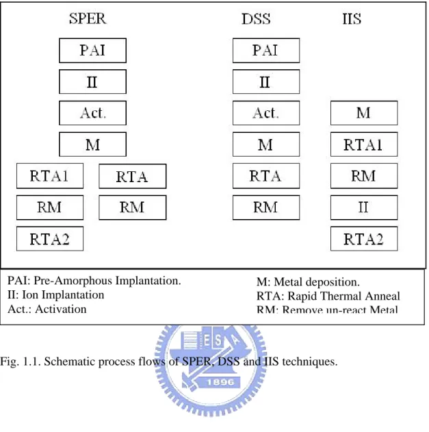
To date, there are three main techniques proposed for low temperature dopant activation, which are Solid Phase Epitaxial Regrowth (SPER) [4,5], Dopant Segregated Schottky junction (DSS) [6,7], and Implant Into Silicide (IIS) [8,9]. We will give a brief introduction to these three techniques at below:
1.2.1 Solid Phase Epitaxial Regrowth
The fabrication process about SPER technique is pre-amorphous crystal silicon to amorphous type and then implanting dopant. Main dosages will remain in
the amorphous region and when activation process is performed, effective dopant activation will be achieved only to the dopant in the amorphous region. The most important concept for why the SPER process could achieve relative low temperature activation (most around the process window 700 to 800 ℃ ) is that dopant in amorphous silicon could activated at the density above the density of their thermal equilibrium solubility in the crystalline silicon [4]. However there are still two drawbacks about the SPER process. First, despite the thermal budget control for SPER, the main parameter should be considered for SPER process is the pre-amorphous depth. From the viewpoint of device fabrication, the pre-pre-amorphous depth determines the junction’s depth. For properly junction depth controlling consideration, a high cost low energy ion implanter is required. Secondly, to fully remove the implantation damage, a relative high thermal budget process [5], higher than activation itself required, is preferred. However, this high temperature process is not easy to control, if this regrowth process does not control well, there will be a negative impact to the junction performance. The implantation damage annealing process will limit the SPER’s process window.
1.2.2 Dopant Segregated Schottky Junction
The fabrication process about DSS technique [6,7] is (a) pre-activation dopant in silicon by traditional method or SPER technique, and (b) change/control the junction from silicon p-n junction, i.e. p+/n junction, to the silicide/p+/n junction. The final junction depth of DSS technique is the silicide thickness plus the diffused junction depth which depends on the silicidation process. The DSS technique takes the advantage over traditional junction fabrication process by three factors. First, dopant segregation phenomenon at silicide/silicon interface will cause dopant piled up at the interface, this factor will increase the effective dopant concentration of the
heavily doped junction. Secondly, the heavily doped region is well confined at a few nano-meter from the silicide interface. Thirdly, the thermal budget for silicidation process could below 700℃(depends on the material of silicide source), it is a low temperature process. Since the thermal budget of silicidation technique is lower than that of SPER process, it seems that the DSS method has lower thermal budget when compared with SPER process. However, since the DSS technique is used to fabricate the S/D regions of the MOS device, it needs to meet the spec of the MOS device at the S/D side, shallow junction. Although the final junction depth determined by silicidation process, the original junction depth is also very important. This is because DSS method must let the original activated junction fully reacted to become silicide, which means that, for well shallow junction controlling, the DSS method must base on the SPER process. As the result, the determination thermal budget for the DSS technique is the same as for the SPER process.
1.2.3 Implant Into Silicide
On the other hand, Implant Into Silicide technique provides an extremely simple process. IIS method forms junction without any additional steps or new manufacturing systems compared to the conventional junction formation process, instead, it just changes the sequence of the junction fabrication steps. As shown in Fig. 1.1, conventionally, silicidation is processed after the S/D junction activation process, but in IIS technique, it inserts the implantation and activation processes between the silicidation processes, i.e. after first silicidation RTA process. Most thermal budgets [8,9] needed in IIS method are below 700℃, and this is important to the integrating for high-k gate dielectric materials. Since some high-k materials [2] start to crystallize at 600℃, IIS could be a candidate to integrate with high-k material with gate first MOSFET fabrication process.
1.3 Motivation
There are many reports showed that they have successfully fabricated p/n junctions using IIS method, such like low contact resistance [10], low reverse current [11], high activation energy [11] and even been integrated in MOS device [12]. Although these researches illustrated very attracting results, the process window of IIS technique for these researches were different far from one to each other, from tens of seconds to a few hours. Is this implying that IIS technique is very robust and have a very wide process window? Although most studies have showed that the device fabricated by IIS method has a good performance, few literatures have been done on the topic of the mechanism of how the junction formation starts and why the IIS technique could achieve high activation at low activation temperature. In these study, we try to discuss and descript the junction formation behavior and some possible mechanisms of IIS technique.
1.4 Thesis Organization
This thesis is mainly composed of two parts. Part I (ch2 MS junction, ch3 M/N+/P junction, and ch4 M/P+/N junction) are focus on the mechanisms related to the junction formation and dopant activation issues of IIS method and Part II (chapter 5,6) tries to find a proper way to interpret the corresponding electrical properties of junctions formed by IIS method (ch5 Electrical Properties of Shallow Junction) and also covers some thermal reliability issue (ch6 Thermal Reliability of Junctions Formed by IIS Method). At the end, a final chapter (ch7) of the summary of this thesis and the future work of this study is also included.
References
[1] ITRS Roadmap 2006 update
[2] G.D. Wilk, R. M. Wallace, and J. M. Anthony: J. Appl. Phys., Vol. 89, 5243, (2001).
[3] C.S. Kang, H.J. Cho, R. Choi, Y.H. Kim, C.Y. Kang, S.J. Rhee, C. Choi, M.S. Akbar, and J.C. Lee:
Electron Devices, IEEE Transactions on, Vol. 51, Issue 2, 220, (2004).
[4] M.J.P. Hopstakena, Y. Tamminga, M.A. Verheijen, R. Duffy, V.C. Venezia, A. Heringa: Applied
Surface Science, Vol. 231–232, pp. 688, (2004).
[5] B.J. Pawlak, R. Lindsay, R. Surdeanu, P.A. Stolk, K. Maex: Proceedings of the 14th International
Conference on Ion Implantation Technology, pages X, (2002).
[6] A. Kinoshita, Y. Tsuchiya, A. Yagishita, K. Uchida and J. Koga: IEEE VLSI, pp. 168, (2004). [7] T.P. Lee, T.Y. Liow, K.M. Tan, E.J Lim, C.S. Ho, K.M. Hoe, M.Y. Lai, T. Osipowicz, G.Q. Lo, G.
Samudra, D.Z. Chi, and Y.C. Yeo: IEEE VLSI , pp. 108, (2007).
[8] D.L. Kwong, T.H. Ku, S.K. Lee, E. Louis, N.S. Alvi, and P. Chou: J. Appl. Phys. Vol. 61, pp. 5084, (1987).
[9] J. Kedzierski, D.Boyd, C. Cabral, Jr., P. Ronsheim, S. Zafar, P.M. Kozlowski, J.A. Ott, and M. Ieong: Electron Devices, IEEE Transactions on, Vol. 52, Issue 1, pp. 220, (2005).
[10] C.C. Wang and M.C. Chen: J. J. Appl. Phys. Vol. 45, pp.1582, (2006). [11] Advanced Micro Devices, Inc. US Patent number-7306998
PAI: Pre-Amorphous Implantation. II: Ion Implantation
Act.: Activation
M: Metal deposition.
RTA: Rapid Thermal Anneal RM: Remove un-react Metal
Fig. 1.1. Schematic process flows of SPER, DSS and IIS techniques.
Chapter 2
MS J
UNCTION
2.1 Introduction
Most efforts to study the Implant Into Silicide (IIS) method were based on p/n junction diode structure, however, before discussing p/n diodes, the properties at the silicide/silicon interface formed by IIS technology should be made clear at first. Since there is always a MS junction exists in series with the p/n junction, unless we know the MS junction properties, we could not fully understand the p/n diodes properties. As a result, we start our effort from discussing the MS junction behavior.
With carefully design of the process parameters, except the potential low temperature activation ability, the IIS method could provide two additional advantages to traditional S/D activation process. First, if the projection range of the implantation is located at silicide, the implantation damage in the silicon region could be minimized. Secondly, like the DSS technique, dopant in the silicide could be piled up at the silicide/silicon interface during the 2nd RTA step of the IIS method. The dopant segregation phenomenon could provide a possibility for the designer to lower the implantation dosage, as a result, the implantation damage could be further lowered.
Since we used the nickel silicide be the metal contact material, it is reported that the phase transition of NiSi to NiSi2 is about 700℃, and with higher temperature
treatment, the silicide will agglomerate. To avoid theses unwanted factors to affect our work, the high temperature treatment in this study is below 700℃. This is also a good process window for most high-k dielectrics [1, 2]. Furthermore, for properly integrating the IIS method and high-k dielectric, lower thermal budget is preferred. In
this study, RTA (Rapid Thermal Annealing) system is adopted, and all thermal treatments were done not more than one minute.
2.2 Methods
SIMShas most frequently been adapted to show the dopant segregation
phenomena at the silicide/silicon interface and the spreading resistance profiling (SRP) method has been used to analyze the dopant concentration at the bulk activated region [3-5]. However, SIMS spectrum does not provide the information about the activation and it is hard using SRP to study the doping profile at the silicide/silicon interface. In order to overcome these difficulties in measurements, in this chapter, we use the metal/semiconductor (MS) diode structure combined with I-V (current-voltage), C-V (capacitance-voltage), and SIMS measurements to explore the high activation ability at the silicide/silicon interface made by the IIS method. For the purpose of checking the activation ability near the silicide/silicon interface, a relative low dosage 1x1013 cm-2 is adapted in this study.
I-V measurement could give the information about the transportation mechanism at the M/S interface, and C-V measurement point a way to evaluate the doping density at the M/S interface. SIMS spectrum and AFM images are used as the reference for the device fabrication.
2.3 Device Fabrication
Stating material is (100) n-type (1 to 10 ohm-cm, phosphorous doped) and (100) p-type (1 to 10 ohm-cm, boron doped) wafer. A 200 nm thick silicon dioxide was thermally grown for isolation. Nickel silicide was formed by two-step rapid thermal
annealing (RTA) process. A 20 nm thick nickel film was deposited by sputter system. All samples were under first step RTA at the condition 400℃ 30s. After removing the unreacted Ni, p-type substrate samples were implanted with BF2 (1x1013 cm-2, 20keV)
and n-type substrate samples were implanted with arsenic (1x1013 cm-2, 10keV). Before thermal coated Al as the back contact, samples were treated with 2nd RTA step 30 seconds at different temperatures from 400 to 650℃, 50℃ per step (400, 450, 500, 550, 600, and 650℃).
2.4. Results and Discussions
2.4.1 SIMS measurement
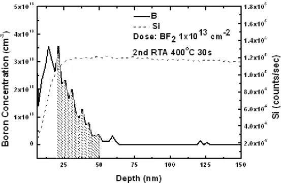
SIMS profile of the BF2 doped sample with 2nd RTA 400℃ 30s is shown in Fig.
2.1, and it provides two messages. First, the peak boron concentration is appeared inside the nickel silicide film suggesting that the projected range at this study is in the silicide, which implies the implantation damage in the silicon is depressed. And secondly, dopant segregation phenomenon can be found at the silicide/silicon interface even at the short period with low temperature annealing (2nd RTA 400℃ 30s). The silicide thickness from SIMS measurement is about 23nm, and this value is confirmed by the SEM inspection.
2.4.2 C-V measurement
In this study, we adapted the capacitance-voltage measurement [6] to analyze the silicide/silicon interface. With depletion approximation, depletion width (W) in the silicon is estimated by
C A K W = sε0
(3.1)
Where Ks is dielectric constant of silicon and A is the MS diode’s contact area. And the effective doping density at depth W is given by
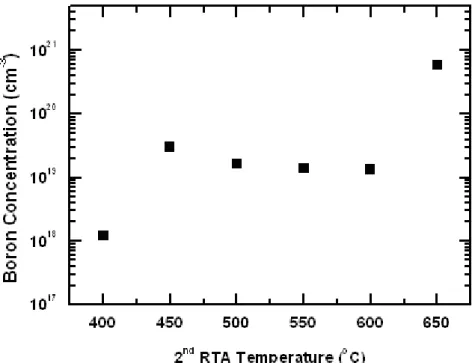
dV C d A qK W N s A / ) / 1 ( 2 ) ( 2 2 0 ε = (3.2) Averaged boron doping density within the depletion region extracted form C-V measurement is illustrated in Fig. 2.2. It shows that with higher 2nd RTA temperature, higher doping density is obtained. From C-V measurement results, two observations can be found. First, even at the lowest activation temperature (400℃), the effective doping density (Neff) is higher than 1018 cm-3, this convinces that IIS is an effective
method to achieve low temperature activation. And secondly, at higher temperature annealing, Neff becomes higher than 1019 cm-3. Silicon begins to become the
degenerate substance at this high doping level, and this property is good for silicide/silicon interface to form an ohmic contact. Furthermore, we compared the integral of the dopant concentration over depths from SIMS and C-V measurement results (nSIMS and nCV) in Fig. 2.3. It shows that the activation percentage (nCV/nSIMS)
is very high. Over 50% dopant was activated over 2nd RTA 450℃. The summation process was taken from Vr = 0 to 0.2V and dopant within the depletion region at V=0 was not summed in the C-V measured data. Samples with high Neff might not be fully
depleted in this voltage range; as a result, under-estimated nCV might occur in these
high Neff samples. There exist an abnormal activation calculation occurred at 2nd RTA
650℃ sample. This may be due to the incorrect high doping density obtained from equation (3.1) and (3.2) that using Boltzmann distribution. The Maxwell-Boltzmann distribution will over-estimate the Neff when the material becomes
degenerate [7] and as the consequence, the activated dopant obtained using Neff will
also be over-estimate. At this study, we only use the Maxwell-Boltzmann distribution to estimate the doping density. Although it may not good enough to extract the real concentration of the sample, it does reflect the high activation ability at the silicide/silicon interface, and shows that near the M/S interface, silicon is undoubtedly turning into the degenerate material.
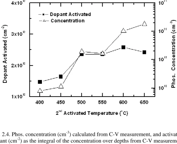
Similarly, phosphorous doped samples exhibit the high activation ability. It can be found in Fig. 2.4 that with above 500℃ 2nd RTA, phosphorous doped samples also achieve high effective doping densities more than 1x1019 cm-3, which make the silicon at the M/S interface to become ohmic contact.
It might be thought strange that why some samples with high concentrations (cm-3) but have lower activated dopant densities (cm-2) shown in Fig. 2.3 and Fig. 2.4. The main reason must be explained by our data analyzing processes.
1. We measured I-V characteristics at different temperatures and the results showed that at lower temperatures (< 35 ℃), the sample behaved different to that at higher temperatures from the Arrhenius plot. We think that samples have Thermionic/Field Emission (TFE) behavior. From the measurements, we had chosen the C-V measurement voltage range in this study to be below 0.2 volt in order to decrease the field emission effects. As a result, the C-V measurements in Fig.2.2 to Fig. 2.4 are at the voltage range from 0V to the reverse biased 0.2V, 5 mV per step.
2. The data used to obtain concentrations (cm-3) are the average concentrations from Vr =0 to 50mV, because these data are close to the M/S interface.
3. The data of densities (cm-2) are the summation from Vr = 0 to 0.2V, which are different to the voltage range used to obtain concentrations (cm-3). [during
summation, Σconcentration (cm-3)*d (cm-1), only concentrations > 1x1016 cm-3 were included].
4. Data shown in Fig. 2.2 to Fig. 2.5 are averaged value of 10 different test devices.
Also, there are two points should be stated:
1. The concentrations (cm-3) are more sensitive to a high measured data than densities (cm-2) will be.
Since densities (cm-2) are obtained from concentration (cm-3)*d (cm-1), where d is negative related to concentrations (cm-3). We think that this is the key point to the question why some samples with high concentrations but have lower activated dopant densities. At Vr = 0 to 0.2V, some samples with high concentrations (cm-3) may not be fully depleted. So the densities (cm-2) collected in this voltage range are truly narrower than the samples with lower concentrations (cm-3). This “narrow behavior” is just because the limitation from the measurement voltage range. We have thought to normalize the densities (cm-2) of all samples at the same integral width, but if we do so, the under-estimated densities (cm-2) at samples with lower concentrations (cm-3) will become serious. At this section, our object is to show that the high activation ratio can be obtained, so we decide to hold out the original data at the cost of under-estimating the densities (cm-2) at samples with higher concentrations. Even though, we still successfully showed that, truly, from the C-V measurements results, IIS proving a high activated doping ability at the silicide/silicon interface.
2.4.3 I-V Measurement
For direct determine if the M/S junction is ohmic contact or not, I-V measurement can be a good reference. The corresponding I-V characteristics of boron doped
samples are illustrated in Fig. 2.5 all samples with 2nd RTA have linear I-V characteristics instead of schottky diodes regulation characteristics, which means that all samples behave more likely to be ohmic contacts than schottky contacts. In addition, the slopes of the I-V curves are increasing when raising the 2nd RTA temperature from 400 to 550℃. Since the silicide after 2nd RTA temperatures at the range between 400 to 650℃ is at the nickel mono silicide phase [8], the sheet resistance is the same at these temperatures. The different characteristics of I-V curves with different 2nd RTA temperatures should be contributed to the differences in contact resistance. This indicates that the contact resistance is decreasing with increasing 2nd RTA temperature. This is in good agreement to C-V measurement result that more boron is activated at higher 2nd RTA temperature and higher 2nd RTA temperature can form better ohmic contact. Phosphorous doped samples have similar I-V behaviors. Both BF2 doped p-type substrate and P doped n-type substrate show
ohmic contact behavior at low temperature activation with nickel silicide as the contact metal using IIS method.
2.4.4 AFM Inspection
Morphology inspection is required to further to clarify that previous C-V and I-V measurement results are not biased by silicide deformation. Samples (n-type substrate, phosphorous doped) without 2nd RTA and with 2nd RTA 30s at different temperatures (400, 500 ,600, and 700 ℃) are prepared. Fig. 2.6 shows the AFM inspection results for these samples (Area: 10μm x 10μm), and all RMS values are around 1nm. No agglomerations are discovered in these samples even at RTA 700 ℃ 30s, which are similar to other groups’ results [8, 9]. Since fluorine can retard nickel silicide film’s agglomeration [10], it is believed that BF2 doped samples can also sustain RTA 700
℃ 30s without agglomeration occur. Since the experiments from 2.4.1 to 2.4.3 are taken under 700 ℃ , it is believed that these results are not biased by silicide agglomeration effect.
2.5 Conclusions
From SIMS measurement, it exhibits that there are high dopant dosages pilled up at the M/S interface due to the dopant segregation phenomenon even under low thermal budget 2nd RTA control. This factor could limit the implantation damage mainly occurred in the silicide layer and provide a better M/S interface. C-V measurement shows that with higher 2nd RTA temperatures at the range 400 to 650℃, higher activation could be achieved at the M/S interface for both boron and phosphorous doped samples. Ohmic contact property could be found in I-V measurements, with higher 2nd RTA temperatures between 400 to 550 ℃ , lower contact resistances are present. AFM inspections shows that no agglomeration of silicide film is occurred under 700 ℃ 30s. From these results, 2nd RTA 500 to 600℃ 30s may be a good process window for IIS method to future integration with high-k dielectric device.
References
[1] G..D. Wilk, R. M. Wallace, and J. M. Anthony: J. Appl. Phys., Vol. 89, pp. 5243, (2001).
[2] C.S. Kang, H.J. Cho, R. Choi, Y.H. Kim, C.Y. Kang, S.J. Rhee, C. Choi, M.S. Akbar, and J.C. Lee:
Electron Devices, IEEE Transactions on, Vol. 51, Issue 2, pp. 220, (2004).
[3] B.J. Pawlak, R. Lindsay, R. Surdeanu, P.A. Stolk, K. Maex: Proceedings of the 14th International
Conference on Ion Implantation Technology, pages X, (2002).
[4] M.J.P. Hopstakena, Y. Tamminga, M.A. Verheijen, R. Duffy, V.C. Venezia, A. Heringa: Applied
Surface Science, Vol. 231–232, pp. 688, (2004).
[5] R. Lindsay, K. Henson, W. Vandervorst, K. Maex, B.J. Pawlak, R. Duffy, R. Surdeanu, P. Stolk, J.A. Kittl, S. Giangrandi, X. Pages and K. van der Jeugd: J. Vac. Sci. Technol. B, Vol. 22, No. 1, pp. 306 (2004).
[6] Dieter K. Schroder: “Semiconductor material and device characterization”, second edition, John
Wiley & Sons, Inc. 1998.
[7] J.S. Blakemore: Solid-State Electronics, Vol. 25, pp. 1067, (1982).
[8] A. Lauwer, J.A. Kittl, M.J.H.V. Dal, O. Chamirian, M.A. Pawlak, M. de Potter, R. Lindsay, T. Raymakers, X. Pages, B. Mebarki, T. Mandrekar, and K. Maex: Materials Science and
Engineering B, Vol. 114-115, pp. 29, (2004).
[9] C.C. Wang and M.C Chen: J. J. Appl. Phys. Vol. 45, pp. 1582, (2006).
[10] A. S. Wong, D. Z. Chi, M. Loomans, D. Ma, M.Y. Lai, W. C. Tjiu, S. T. Chua, C. W. Lim, and J. E. Greene: Appl. Phys. Lett., Vol. 81, pp. 5138, (2002).
Fig. 2.1. SIMS profile of the BF2 doped p-type substrate, with 2nd RTA 400℃ 30s.
The dopant segregation phenomenon can be found at about 23nm from surface. The shadow area from 23nm to about 50nm is about 5x1012 cm-2, which is defined as dopant implanted in Fig. 2.3.
Fig. 2.2. Boron concentrations at different 2nd RTA temperatures extracted by C-V method
Fig. 2.3. Dopant (cm-2) as the integral of the concentration over depths from C-V and SIMS profile (dopant activated and dopant implanted) versus different 2nd RTA temperatures.
Fig. 2.4. Phos. concentration (cm-3) calculated from C-V measurement, and activated dopant (cm-2) as the integral of the concentration over depths from C-V measurement at different 2nd RTA temperatures.
Fig. 2.5. I-V characteristics of boron doped samples. All samples with 2nd RTA behave more likely to ohmic contacts than schottky contacts.
Fig. 2.6. AFM images show NiSi surface morphology with 30 second 2nd RTA at (a) 400 ℃ (b) 500 ℃ (c) 600 ℃ (d) 700 ℃.
Chapter 3
N
+/P J
UNCTION
3.1 Brief Introduction and Design Idea
Based on our previous work [1], we could conclude that even at very low dosage (1x1013 cm-2), dopant activated at the silicide/silicon interface could drive the MS junction to become ohmic like. These experiment results showed that even with low temperature thermal treatment, junction formed by IIS [2-4] technique still had high dopant activation ability. But what is most important to us is that why IIS technique could exhibit this unusual property? There are no researches to answer this mechanic before.
To answer this question, first of our assumption is refer to the SPER [5-8] process. SPER process gives a good explanation of why dopant can be activated at lower temperature than traditional junction formation process. If there any linkage between SPER and IIS techniques? It is known that there will be an amorphous layer formed at silicide/silicon interface during the silicidation process. It is reasonable that what is happened in SPER process will also occur in IIS process. This provides the base of low temperature activation behavior for IIS technique. In addition, IIS usually needs less activation temperature comparing to SPER process. Our second assumption to the IIS technique is that silicide could lower the energy required for the SPER process. This factor is less discussed in CMOS process, but for TFT process, metal induced crystallization or lateral crystallization (MIC/MILC) is often been studied.
At this part, heavily doped phosphorous (5x1015 cm-2) is applied to our test device. Such a high dosage is commonly adapted in the traditional junction
fabrication process. The projection range of the implantation was designed to locate in the silicide to let the implantation damage in silicon be minimized. The constraint for thermal treatments is the same as that in the chapter 1. Different to the metal/silicon interface discussed in chapter 1, chapter 2 focus on the silicide/N+/P test structures.
3.2 Device Fabrication
3.2.1 Device fabrication for I-V, C-V, SIMS measurements
Thirty-nanometer silicon dioxide was thermally grown on (100) p-type silicon wafer as the isolation oxide, after defining the active region, a 20nm nickel film was then deposited by E-gun evaporation system. All samples were treated with 1st RTA 350℃ 30s, after un-reacted Ni was removed, all samples were ion implanted with phosphorous (doping density: 5x1015 cm-2), followed different 2nd RTA temperature treatments 60 seconds from 400℃ to 650℃, 50℃ per step. At the final step, Al was thermally coated as back contact. No post metal annealing was treated for thermal budget control consideration.
3.2.2 Device fabrication for FPP measurements
For four points probe test structure, starting material was (100) p-type silicon wafer, too. After thermal oxidation and active regions definition, 20nm nickel was deposited by e-gun system. Following processes were the same as described in section 3.2.1. However, for FPP test structure, after 2nd RTA, NiSi was removed using silicide etch solution (the etch selectivity of NiSi to bare Si is larger than 50). At the final step, Al was thermally coated as back contact. No post metal annealing was treated for thermal budget control consideration.
3. 3 Results and Discussions
3.3.1 C-V measurement
The effective phosphorous concentration (Neff) estimated from C-V measurement
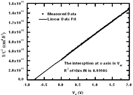
[9] is demonstrated in Fig. 3.1. The measured capacitance is composed by of three different capacitances in series, silicide/silicon (M/S) junction capacitance, N+/P junction capacitance, and back contact capacitance. Based on the results in chapter 2 (see also reference 10), it shows that there present a high dopant activation level at the M/S interface formed by IIS method, either it will become an ohmic contact or exits a relative large capacitance compared to the N+/P junction capacitance where the lightly doped substrate dominate the small capacitance value. The M/S capacitance term could be neglect with little influence in the analysis. On the other hand, the area of the back contact is about the full wafer size, which is several orders of magnitude larger than the area of N+/P junction, so the capacitance at the back contact can also not take into consideration. As the result, the measured capacitance was mainly contributed due to p-sub depletion junction at the N+/P junction. From analyzing the C-V data, the p-sub doping density can be obtained from the differential capacitance-voltage profiling technique [9]. Fig. 3.1 shows the relationship between the depletion capacitance and the applied reverse voltage, the building voltage of the N+/P junction can be obtained from the projection of the 1/C2-V curve to where 1/C2 =0. The high linearity of the 1/C2-V curve implies that the abruptness of the N+/P junction is good and is suitable to use the abrupt junction formula to express the experimental results. The Neff is then calculated from the averaged substrate doping density and the
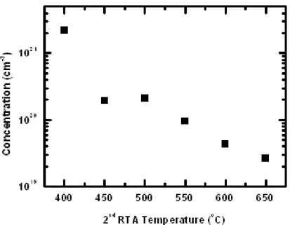
building voltage. The relation of Neff to the 2nd RTA temperature is shown in Fig. 3.2,
it seems that the Neff presents at the N+/P interface is negatively related to the 2nd RTA
temperature. The lowest Neff extracted at this study is above 1019 cm-3, which is four
order larger than the substrate doping density. This supports the assumption that the capacitance measured is mainly due to the depletion in substrate at the N+/P junction.
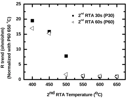
3.3.2 FPP and SIMS measurements
Some papers appointed that defects might cause dopant deactivated [11,12] at higher RTA temperature. However, from the study about the M/S junction [10], we did not find significant deactivation to take place at the silicide/silicon interface at the same process window in this study. In order to make clear what is the origin of the decreased Neff, a test structure designed for FPP measurement is adapted. By
removing nickel silicide using silicide etch solution (the etch selectivity of nickel silicide to bare Si is larger than 50 in our test), the results of measured resistance are displayed in Fig. 3.3. It shows that the resistances become smaller with higher 2nd RTA temperatures, which means that either doping concentration or the junction depth is extended with higher 2nd RTA temperature. Comparing the result to the SIMS profile in Fig. 3.4, suggesting that the lower Neff measured at higher temperature is
mainly due to that where the N+/P interface presented are at the deeper position away from the M/S interface. The result implies that the dopant activation behavior is starting from the NiSi/Si interface and then extended to the silicon substrate. If the high activated doping concentration is related to the SRER process as we assumed in the previous chapter, it is recommended that the SPER process is starting from the M/S interface. As a consequence of C-V, FPP, and SIMS measurements, the suggested phosphorous activation behavior of the IIS method is illustrated in Fig. 3.5. 3.3.3 I-V measurement
In addition to analyze the junction forming behavior, I-V measurement are adapted. The N+/P diode I-V measurement results are summarized as Jon (at VA = -1V) and Joff
(at VA = 2V) exhibited in Fig. 3.6. The sample with 2nd RTA 550℃ 60s treatment has
the lowest Joff value among all samples. The high Joff current densities presented at 2nd
RTA temperature below 500℃ are explained as that there may exist high defect densities at the P/N junction interface. The defects may originate from the remained amorphous region where is still not recrystallized due to the short activation time or the low activation temperature. As the result, with increasing 2nd RTA temperatures, the SPER process continuous going, and the Joff currents decreased. At 2nd RTA 550
℃ 60s, the SPER process seen to be completed (this can be observed by the relative consistent resistances measured in FPP method, see Fig. 3.3), the sample exhibits the maximum on/off ratio. However, the on/off ratios (Fig. 3.6) and Neff (Fig. 3.2)
diminish at 2nd RTA higher than 550℃ 60s. Since the SPER process looks like completed above 2nd RTA 550℃ 60s, the facts described above may originated by defect (dislocations start to form at the temperature range from 500 to 600℃ [13]) itself or by some defect induced dopant deactivation at the P+/N interface. In addition, deactivation from phosphorous super-saturated solubility to thermal equilibrium solubility in silicon [14] might also play an important role when the thermal budget is higher than which required for SPER process completion. (The experiments of thermal stability about dopant super-saturated will be given in future publication.)
3.4 Conclusions
With the starting ideas that SPER and metal enhanced crystallization are the main responses to the high activation ability with IIS method in low activation temperature, we combine the SIMS, C-V, FPP, and I-V measurements to construct the doping activation behavior of the IIS method. All experiment results suggested that SPER process is starting from the M/S interface and extend into the silicon substrate. The best N+/P interface is formed when SPER process is complete. After SPER process finished, samples with additional thermal budget treatment above 550℃ cause the defect formation at the bulk silicon and the dopant deactivation phenomenon may occur, both factors will decay the N+/P junction’s performance. Sample treated with 2nd RTA 550 ℃ 60s forms the best N+/P junction among all controls in this study.
References
[1] K.M. Chang, J.H. Lin, and C.Y. Sun: Applied Surface Science, Vol. 154, pp. 6151, (2008). [2] B.S Chen and M.C. Chen: Electron Devices, IEEE Transactions on, Vol. 43, Issue. 2, pp. 258,
(1996).
[3] D.L. Kwong, T.H. Ku, S.K. Lee, E. Louis, N.S. Alvi, and P. Chou: J. Appl. Phys. Vol. 61, pp. 5084, (1987).
[4] J. Kedzierski, D.Boyd, C. Cabral, Jr., P. Ronsheim, S. Zafar, P.M. Kozlowski, J.A. Ott, and M. Ieong: Electron Devices, IEEE Transactions on, Vol. 52, Issue 1, pp. 220, (2005).
[5] J. Foggiato, W.S. Yoo, M. Ouaknine, T. Murakami, and T. Fukada: Materials Science and
Engineering B, Vol. 114–115, pp. 56, (2004).
[6] A. Steegen, and I. De Wolf, K. Maex: J. Appl. Phys., Vo1.86, No. 8, pp. 4290, (1999).
[7] B.J. Pawlak, R. Lindsay, R. Surdeanu, P.A. Stolk, K. Maex: Proceedings of the 14th International
Conference on Ion Implantation Technology, pages X, (2002).
[8] R. Lindsay, K. Henson, W. Vandervorst, K. Maex, B.J. Pawlak, R. Duffy, R. Surdeanu, P. Stolk, J.A. Kittl, S. Giangrandi, X. Pages and K. van der Jeugd: J. Vac. Sci. Technol. B, Vol. 22, No. 1, pp. 306 (2004).
[9] Dieter K. Schroder: “Semiconductor material and device characterization”, second edition, John
Wiley & Sons, Inc. Chapter 2, 1998.
[10] K.M. Chang, J.H. Lin, and C.Y. Sun: Applied Surface Science, Vol. 154, pp. 6155, (2008). [11] T.E. Seidel and A.U. MacRae: First Intl. Conf. on Ion Implantation, (1971).
[12] K. Larsen, V. Privitera, S. Coffa, F. Priolo, S. U. Campisano, and A. Carnera: Physical Review
Letters, Vol. 76, No.9, pp.1493, (1996).
[13] S. Wolf, and R.N. Tauber: “Silicon processing for the VLSI era”, second edition, Lattice press, Vol. 1, Chapter 10, 2000.
[14] Y. Takamura, S.H. Jain, P.B. Griffin, and J.D. Plummer: J. Appl. Phys., Vo1. 86, No. 1, pp. 230, (2002)
Fig. 3.1. An example of the measured1/C2–V curve, the sample was treated with 2nd RTA 650℃ 60s.
Fig. 3.2. Phos. doping density estimated from C-V measurement with different 2nd RTA temperatures.
400 450 500 550 600 650 0 5 10 15 20 25 R t rend (ohm/ohm) (N orm a li z ed w it h P6 0 6 50 o C)
2nd RTA Temperature (oC) 2nd RTA 30s (P30) 2nd RTA 60s (P60)
Fig. 3.3. Relative resistance ratio measured with FPP test structures at different 2nd RTA conditions
Fig. 3.4. SIMS profile of phosphorous doped sample treated with 2nd RTA 650℃ 60s.
Lower 2
ndRTA
Temperature
N
i
S
i
S
u
b
.
N
i
S
i
S
u
b
.
Higher 2
ndRTA
Temperature
Activated region
Lower 2
ndRTA
Temperature
N
i
S
i
S
u
b
.
N
i
S
i
S
u
b
.
Higher 2
ndRTA
Temperature
Activated region
Fig. 3.5. The behavior of phosphorous activation is shown schematically. The P/N junction interface becomes deeper away from M/S interface with higher 2nd RTA temperature.
Fig. 3.6. Absolute Jon, Joff, current density and on/off ratio measured at different 2nd
RTA temperatures.
Chapter 4
P
+/N J
UNCTION
4.1 Brief Introduction and Design Idea
For the purpose to confirm the ideas made in chapter 2 (SPER and metal assisted metallization construct the low temperature dopant activation ability of IIS technique) and in chapter 3 (The SPER is starting from silicide/silicon interface and then extended into the silicon substrate) are valid, we designed an experiment similar to that in chapter 3 but differs in the implantation projection range design and the junction type. Boron was adapted as the implanted dopant in this study, due to its fast diffusion ability, and as a result the junction now we were treated was changed to silicide/P+/N type. The projection range of this study was changed from in silicide (as in chapter 2 and chapter 3 did) to in the silicon. Since the peak dopant densities was located in the silicon region, we expected to see that with the C-V measurement, we could observe the “moving junction” behavior suggested in chapter 3.
4.2 Experiments
4.2.1 Device fabrication for I-V, C-V, SIMS measurements
Starting material was (100) n-type silicon wafer, after thermal oxidation and active regions definition, backside of the wafer was implanted with phosphorous 5x1015 cm-2 and annealed with furnace at 1000℃ 30 min. TaN 100 nm was sputtered on as the back contact. After dipped dilute HF to remove the native oxide at the active region, 20nm nickel was deposited by e-gun system. All samples were treated with 1st
RTA at 350℃ 30s, after unreacted Ni removed, all samples were ion implanted with BF2 5x1015 cm-2. Then, samples were treated at 2nd RTA 60s with different
temperatures from 400℃ to 650℃, 50℃ per step.
4.2.2 Device fabrication for FPP measurements
For four points probe test structure, starting material was (100) n-type silicon wafer, too. After thermal oxidation and active regions definition, 20nm nickel was deposited by e-gun system. Following processes were the same as described in section 4.2.1. However, for FPP test structure, after 2nd RTA, NiSi was removed using silicide etch solution (the etch selectivity of NiSi to bare Si is larger than 50). At the final step, Al was thermally coated as back contact. No post metal annealing was treated for thermal budget control consideration.
4.3. Results and Discussion
4.3.1 SIMS and C-V measurements
In comparison with N+/P junction behavior studied in our previous work (reference 5, where the projected range is in the nickel silicide), a different doping profile is adapted in this study. As shown in Fig. 4.1, there are two peaks presented in SIMS profile (after 2nd RTA 650℃ 60s). Peak 1 is formed due to dopant segregation [6] phenomena (NiSi film is about 23nm thick determined by SEM inspection), and Peak 2 is the projection range of this implantation.
From previous understanding [5], the effective boron concentration (Neff)
presented at the P/N interface estimated from C-V measurement in this study would not decrease monochromatically with the increasing 2nd RTA temperatures, instead,
Neff measured from increase 2nd RTA temperatures should have the trend such like
some part of the SIMS profile. The C-V measurement result is demonstrated in Fig. 4.2, boron has the similar doping profile (but lower density due to not fully activated) to which obtained in SIMS measurement. This result supports our previous observation in chapter 3 that doping activation of the IIS method is starting from silicide/silicon interface toward the silicon substrate. Substrate doping densities extracted from C-V measurements are also shown in the Fig. 4.2 as a reference. It shows that phosphorous have a bit higher concentrations below 500℃ 2nd RTA. This behaviour might be due to samples treated at lower 2nd RTA temperatures have narrower activated region from the edge of NiSi/Si (M/S) interface, and there are some doping segregation phenomena of phosphorous at the M/S interface. As a result, samples with lower 2nd RTA temperatures, the P/N interface are closer to M/S interface than samples with higher 2nd RTA temperatures, and have a higher substrate concentration due to the doping segregation affect. This double confirms our previous observation in chapter 3.
4.3.2 I-V and FPP measurements
Fig. 4.3 shows the I-V measurement results of samples fabricated in section 4.2.1. The forward current (IF) is defined at sample with 1V forward bias voltage, and
the reverse (IR) current is defined at sample with 2V reverse voltage. From the IF/IR
ratio, it seems that the sample with 2nd RTA 550℃ 60s has the best performance at this measurement. The better performance of 2nd RTA 550℃ 60s than those samples with lower 2nd RTA temperatures can be contributed to two reasons. First, the activation process will also re-crystallize the amorphous layer at silicide/silicon interface caused by silicide formation process. With higher thermal budget, the better
re-crystallization interface can be formed. Secondly, as shown in Fig. 4.1 and Fig. 4.2, the P+/N junction position of 2nd RTA 550℃ 60s sample might be beyond the point 2 appeared in Fig. 4.1, where less doping defects (unactivated dopant and silicon interstitials) are present. However, the I-V behaviour above 550℃is different to those observed about N+/P junction in Fig 3.6, in N+/P case, above 550℃, IF/IR ratios
decreased with increasing 2nd RTA temperature.
To explain the I-V behaviour above 550℃, some other information about the junction formation should be measured as the reference. In Fig. 4.4, the relative resistance of these samples (after NiSi removed) measured with FPP test structure is displayed. The resistance reflects the combination interactions of the doping activation level and the junction depth. All resistances are normalized to the lowest measured value (2nd RTA 650 ℃ 60s). It exhibits that the resistance decreases gradually but has an abrupt decrease at 650℃ for N30 samples (treated with 2nd RTA 30s) and at 600℃ for N60 samples (treated with 2nd RTA 60s). In addition, the lowest resistance values measured in N30 and N60 samples are almost the same at the original data. This implies that above 2nd RTA 650℃ 30s or 2nd RTA 600℃ 60s, the bulk activation of boron is higher than the substrate doping density, and the p-type junction extended far into the substrate. As a result, the resistances measured under this bulk activation [7] condition are very similar. Bulk activation behaviour dominates the P+/N junction formation at high thermal budget conditions. This explains the difference of the N+/P and P+/N junction’s I-V behaviours above 550℃. In N+/P case, the performance of junction formed at high thermal budget condition is dominated by defect formation or dopant deactivation, but for P+/N case, bulk activation behaviour dominates.
The low IF/IR ratio of 600℃ 2nd RTA sample (N600) in this study is due to the
low forward current density measured at VA = 1V. Fig. 4.5 shows the J-V curve of
some samples treated at 2nd RTA 550℃ 60s (N550-1), 600℃ 60 s (N600-1), and 650 ℃ 60 s (N650-1). The ideality factors of these three samples are all round 1.02. The low JA of 1 is explained as follows: the law of junction is violated first of
N600-1, which implies the voltage drop in the bulk regions occurring at lowest forward voltage in N600-1 sample. This means that the built-in voltage (Vbi) of the N600-1 sample is lowest among these samples. This observation confirmed the measured C-V data in Fig. 4.2, the Neff is lowest at 2nd RTA 600℃ 60s sample.
Besides, from Fig. 4.5, it is showed that J-V behaviour of N550-1 sample is different to the others. This doubly verified that higher than 2nd RTA 550℃ 60s activation condition, the junction formation mechanism is much different. The N600 and N650 samples have lower leakage current at low reverse biased voltage due to lower defect densities presented at the junction depletion region. Bulk activation behavior extended the P/N junction far from the implantation caused defect region (i.e. Peak 2 in Fig. 4.1). Although the N600 and N650 samples take the advantage of the good electrical properties, they are not met the shallow junction requirement.
For more comprehensive understanding the P+/N junction formation process, comparing with N+/P junction formation in chapter 3 and the silicide/silicon interface formation processes in chapter 2 is needed. First, the boron activation densities are about 1017 to 1018 cm-3 in this study, however, for the N+/P case, phosphorous could achieve 1019 to 1021 cm-3 doping activation level depending on different process conditions (Fig. 3.2). On the other side, boron activation densities near the silicide/silicon surface could also achieve 1019 to 1021 cm-3 doping activation level as shown in Fig 2.2 [8]. These two observations suggested that the activation abilities for
boron and phosphorous are similar in metal assisted re-crystallize region (near the silicide/silicon interface). But a distance from the M/S interface, near the projection range located in silicon side in this study, where activation mainly correspond to the SPER [9] technique only, the dopant activation ability (1017 to 1018 cm-3) is much lower than which with the metal assisted activation region (1019 to 1021 cm-3). In short, metal assisted activation is more effective than SPER region at the temperatures below 600℃.
4.4 Conclusions
From the experiment results discussed in section 4.3.1 and 4.3.2, the activation of P+/N junction formed with IIS method could be divided into three different mechanisms. First, near the silicide/silicon interface, metal assisted activation is presented, and secondly, at the heavily doped region where SPER caused activation behavior is observed. Finally, with higher activation temperature, above 600℃ in this study, bulk activation dominates the junction’s position and its behavior. Boron could be activated at an effective doping density about 7x1017 cm-3 extracted from C-V measurement under 2nd RTA 450℃ 60s with the SPER caused activation mechanism. Among all process conditions in this work, samples treated at 2nd RTA 550℃ 60s have the best junction electrical characteristics before the bulk activation behavior dominates the device’s properties.
References
[1] C.S. Kang, H.J. Cho, R. Choi, Y.H. Kim, C.Y. Kang, S.J. Rhee, C. Choi, M.S. Akbar, and J.C. Lee:
Electron Devices, IEEE Transactions on, Vol. 51, issue 2, pp. 220, (2004).
[2] F.C. Shone, K.C. Saraswat, and J.D. Plummer, IEDM Tech. Dig., pp. 407, (1985). [3] C.C Wang, Y.K Wu, W.H Wu and M.C Chen: Jpn. J. Appl. Phys. Vol.44, pp. 108, (2005).
[4] C.P Lin; Y.H Hsiao, and B.Y Tsui: Electron Devices, IEEE Transactions on, Vol. 53, issue 12, pp. 3086, (2006).
[5] K.M. Chang, J.H. Lin, and C.H. Yang: Applied Surface Science, Vol. 154, pp. 6155, (2008). [6] C. Y. Ting and S.S Iyer: Proc. 5th IEEE Int. VLSI Multilevel Interconnection Conf., pp.307, (1995).
[7] R. Lindsay, K. Henson, W. Vandervorst, and K. Maex, B. J. Pawlak, R. Duffy, R. Surdeanu, and P. Stolk, J. A. Kittl, S. Giangrandi, X. Pages and K. van der Jeugd: J. Vac. Sci. Technol. B, Vol. 22, issue 1, pp. 306-311, (2004).
[8] K.M. Chang, J.H. Lin, and C.Y. Sun: Applied Surface Science, Vol. 154, pp. 6151, (2008).
[9] M.J.P. Hopstakena, Y. Tamminga, M.A. Verheijen, R. Duffy, V.C. Venezia, A. Heringa: Applied
0 20 40 60 80 100 1E19 1E20 1E21 1E22 Boron Conce n tr at ion (c m -3 ) Depth (nm) 1 2 With 2nd RTA 650oC 60s
Fig. 4.1. SIMS profile of boron concentration with 2nd RTA 650℃ 60s
400 450 500 550 600 650 1016 1017 1018 7x10¹⁴ 8x10¹⁴ 9x10¹⁴ 1x10¹⁵ Boron Co nce n tration (cm -3 ) Temperature (oC) Boron Concentration Substrate Co nce n tration (cm -3 ) Substrate Concentration
400 450 500 550 600 650 105 106 107 108 I F /I R Rati o (A/ A ) 2nd RTA Temperature (oC) I F / IR Ratio where I F is measured at VF=1V and IR is measured at VR= 2V
Fig. 4.3. IF/IR ratio with 2nd RTA 60s at different temperatures
Fig. 4.4. Relative resistance ratio measured with FPP test structures at different 2nd RTA conditions 400 450 500 550 600 650 1 10 100 R tre nd (o hm /ohm) (norm a lized w it h N6 0 65 0 C) 2nd RTA Temperature (oC) 2nd RTA 30s (N30) 2nd RTA 60s (N60)
-2 -1 0 1 2 10-10 10-9 10-8 10-7 10-6 10-5 10-4 10-3 10-2 10-1 100 101 N550-1 N600-1 N650-1 J A (A/c m 2 ) V A (V)
Fig. 4.5. The J-V characteristics of N550-1, N600-1, and N650-1 samples