IEEE TRANSACTIONS ON ELECTRON DEVICES, VOL. 55, NO. 12, DECEMBER 2008 3489
Characteristics of HfO
2
/Poly-Si Interfacial Layer
on CMOS LTPS-TFTs With HfO
2
Gate Dielectric
and O
2
Plasma Surface Treatment
Ming-Wen Ma, Tsung-Yu Chiang, Woei-Cherng Wu, Tien-Sheng Chao, Senior Member, IEEE, and Tan-Fu Lei
Abstract—In this paper, high-performance
complementary-metal–oxide–semiconductor low-temperature polycrystalline-silicon thin-film transistors (CMOS LTPS-TFTs) with HfO2 gate dielectric are fabricated on one wafer for the first time. Low threshold voltage and excellent subthreshold swing can be achieved simultaneously for N- and P-channel LTPS-TFTs without hydrogenation. In addition, the impacts of the HfO2/poly-Si interfacial layer on N- and P-channel LTPS-TFTs are also specified. In order to enhance the characteristics of HfO2 LTPS-TFT further, oxygen plasma surface treatment is employed to improve the interface quality and passivate the defects of channel grain boundaries, thus increasing the carrier mobility and reducing the phonon scattering. The CMOS LTPS-TFTs with HfO2gate dielectric and oxygen plasma treatment would be suitable for the application of system-on-panel.
Index Terms—High-κ, low-temperature polycrystalline-silicon
thin-film transistors (LTPS-TFTs), oxygen plasma, system-on-panel (SOP), 3-D integration.
I. INTRODUCTION
H
IGH-PERFORMANCE low-temperature polycrystalline-silicon thin-film transistors (LTPS-TFTs) have been widely investigated for the application of 3-D device inte-gration on very large scale inteinte-gration technology and the driving integrated circuits on glass panel [1]–[4]. In order to achieve high-performance characteristics of LTPS-TFTs with low threshold voltage |VTH|, high field-effect mobility μFE,and low subthreshold swing (S.S.), hydrogen-related plasma treatment is usually used to passivate the defects of poly-Si channel film and SiO2/poly-Si interface [5]–[8]. Unfortunately,
the introduction of hydrogen would result to the reliability issue of LTPS-TFTs [8]–[11]. The employment of high-κ materials as the gate dielectric of LTPS-TFTs has been proposed to be an effective way to improve the electrical characteristics of LTPS-TFTs without any defect passivation methods [12]–[15]. For the application of system-on-panel (SOP) and 3-D circuit inte-gration, complementary-metal–oxide–semiconductor (CMOS)
Manuscript received April 17, 2008; revised August 18, 2008. Current version published November 26, 2008. This work was supported by National Science Council, Taiwan, under Contract NSC-97-2221-E-009-152-MY3. The review of this paper was arranged by Editor H. S. Momose.
M.-W. Ma and T.-F. Lei are with the Institute of Electronics, National Chiao Tung University, Hsinchu 300, Taiwan.
T.-Y. Chiang, W.-C. Wu, and T.-S. Chao are with the Department of Electrophysics, National Chiao Tung University, Hsinchu 300, Taiwan (e-mail: [email protected]).
Color versions of one or more of the figures in this paper are available online at http://ieeexplore.ieee.org.
Digital Object Identifier 10.1109/TED.2008.2006543
LTPS-TFTs should be studied simultaneously. However, the fabrication of N- and P-channel LTPS-TFTs with high-κ gate dielectric on one wafer has not been reported. In this paper, the N- and P-channel LTPS-TFTs with HfO2gate dielectric are
demonstrated simultaneously for the first time. In addition, the growth of a SiO2-like interfacial layer (IL) at the high-κ/poly-Si
interface is generally observed while the high-κ materials are deposited on the poly-Si surface [12]–[14]. In this paper, the impacts of the HfO2/poly-Si IL on the electrical characteristics
of HfO2 CMOS LTPS-TFT are specified and compared with
conventional SiO2CMOS LTPS-TFTs.
In addition to the employment of high-κ gate dielectric, the oxygen plasma treatment has been proposed to improve the electrical characteristics of TFTs [16]–[20]. The improvements of TFTs after oxygen plasma posttreatment are due to the defect passivation of grain boundaries in the poly-Si channel film [16], [17] and the good quality of the oxide grown by oxidizing the poly-Si surface by oxygen plasma pretreatment [18]–[20]. In this paper, the oxygen plasma is used to study the impacts of the HfO2/poly-Si IL on CMOS LTPS-TFTs with HfO2 gate
dielectric.
II. EXPERIMENTALPROCEDURE
The fabrication of devices started by depositing a 50-nm undoped amorphous-Si (α-Si) layer at 550◦C in a low-pressure chemical vapor deposition system on Si wafers capped with a 500-nm thermal oxide layer. Then, the 50-nm α-Si layer was recrystallized by the solid-phase crystallization process at 600 ◦C for 24 h in a N2 ambient. Furthermore, a 500-nm
plasma-enhanced chemical vapor deposition oxide (PECVD-SiO2) was deposited at 300◦C for device isolation. The device
active region was formed by patterning and etching the isolation oxide. As shown in Fig. 1(a), the source and drain (S/D) region in the active device region was implanted with phosphorus (15 keV at 5×1015cm−2) and boron (10 keV at 5×1015cm−2) for N- and P-channel LTPS-TFTs, respectively. The S/D region was activated at 600 ◦C for 24-h annealing in a N2 ambient.
Then, oxygen plasma surface treatment was performed for 0, 5, and 15 min at 300◦C with a power density of 1.6 mW/cm2in O2 gas, as shown in Fig. 1(b). The flow rate was 100 sccm at
pressure of 67 Pa. A 50-nm HfO2with effective oxide thickness
of approximately 10.8 nm was deposited by electron-beam evaporation system at room temperature. In addition, a 49.3-nm PECVD SiO2was deposited at 300◦C as the gate dielectric of
conventional CMOS LTPS-TFTs, which are used to compare
Fig. 1. Cross-sectional view of CMOS LTPS-TFTs with HfO2gate dielectric
and oxygen plasma surface treatment.
with CMOS LTPS-TFTs with HfO2 gate dielectric. After the
patterning of S/D contact holes, aluminum was deposited by thermal evaporation system as the gate electrode and S/D contact pad. Finally, the TFT devices were completed by the contact pad definition, as shown in Fig. 1(c). Devices with gate length (L) and width (W ) of 10 and 100 μm are measured, respectively. The threshold voltage|VTH| is defined as the gate
voltage at which the drain current reaches 10 nA× W/L and
|VD| = 0.1 V. The field-effect mobility (μFE) is extracted from
the maximum transconductance (Gm)
III. RESULTS ANDDISCUSSION
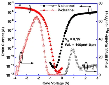
Fig. 2 shows the transfer characteristics (ID–VG and
field-effect mobility μFE) of CMOS HfO2 LTPS-TFTs without
oxygen plasma surface treatment. Some important parameters of CMOS HfO2 LTPS-TFTs without oxygen plasma surface
treatment and of conventional CMOS LTPS-TFTs with SiO2
gate dielectric are also listed in Table I. The threshold voltage
|VTH| and S.S. are reduced significantly while the SiO2 gate
dielectric is replaced by HfO2. Larger gate capacitance density,
which is achieved by replacing the SiO2gate dielectric by HfO2
due to the higher relative dielectric constant of HfO2, can attract
more carriers with a smaller gate voltage to turn on the LTPS-TFTs. In addition, CMOS LTPS-TFTs with HfO2gate
dielec-tric have higher electron and hole field-effect mobility μFEthan
CMOS LTPS-TFTs with SiO2gate dielectric. It indicates that
the native growth of a SiO2-like IL between the HfO2and
poly-Si has better interface quality than the deposited-poly-SiO2/poly-Si
interface [12]–[15]. Because the poly-Si channel film has a rough Si surface and lots of dangling bonds and strain bonds on the surface of the poly-Si channel film, the native growth of the SiO2-like IL of the HfO2LTPS-TFT can terminate these
defects and lead to better performance of LTPS-TFT.
Fig. 2. Transfer characteristics (ID–VGand field-effect mobility μFE) of
CMOS HfO2LTPS-TFTs without oxygen plasma surface treatment.
TABLE I
IMPORTANTPARAMETERS OFCMOS HfO2LTPS-TFTs WITHOUT
OXYGENPLASMASURFACETREATMENT AND OFCONVENTIONAL
CMOS LTPS-TFTs WITHSiO2GATEDIELECTRIC
For the characteristics of CMOS LTPS-TFTs with HfO2gate
dielectric, as shown in Table I and Fig. 2, the hole field-effect mobility μFEis higher by about 130.4% than the electron
field-effect mobility μFE, which is different from the conventional
CMOS LTPS-TFTs with SiO2gate dielectric wherein the hole
field-effect mobility μFE is lower by about 24.1% than the
electron field-effect mobility μFE. It means that the IL of
the HfO2/IL/poly-Si interface has different characteristics from
that of the deposited-SiO2/poly-Si interface. It is well known
that the field-effect carrier mobility μFE is dominated by the
trap states near the band-tail region [7]. A higher hole field-effect mobility μFEthan the electron field-effect mobility μFE
for HfO2LTPS-TFTs indicates that there are less tail trap states
near the valence band than there are near the conduction band. It implies that the native growth of the SiO2-like IL of the
HfO2/poly-Si interface can terminate the tail trap state density
near both the conduction band and the valence band, and more trap density is terminated near the valence band than near the conduction band. Fig. 3 shows the output characteristics (the
ID–VDcurve) of CMOS LTPS-TFTs with HfO2gate dielectric.
A significantly higher driving current of the P-channel HfO2
LTPS-TFT than the N-channel HfO2 LTPS-TFT is obtained,
which consists with the behavior of field-effect mobility μFE
of HfO2LTPS-TFTs. It indicates that the P-channel LTPS-TFT
is more suitable for the driving device of display pixel than the N-channel LTPS-TFT if a HfO2 material is used as the gate
MA et al.: CHARACTERISTICS OF INTERFACIAL LAYER ON CMOS LTPS-TFTS 3491
Fig. 3. Output characteristics (ID–VGcurve) of CMOS LTPS-TFTs with
HfO2gate dielectric.
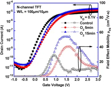
Fig. 4. Transfer characteristics (ID–VGand field-effect mobility μFE) of the
N-channel HfO2LTPS-TFT with and without oxygen plasma surface treatment.
In addition to the intrinsic characteristics of LTPS-TFTs with HfO2 gate dielectric, oxygen plasma surface treatment is
em-ployed to study the impacts of the oxidized IL of HfO2/poly-Si
interface by oxygen plasma on the CMOS LTPS-TFT with HfO2 gate dielectric. Figs. 4 and 5 show the transfer
char-acteristics (ID–VG and field-effect mobility μFE) of N- and
P-channel HfO2 LTPS-TFTs, respectively, with and without
oxygen plasma surface treatment. Some important parameters of CMOS HfO2LTPS-TFTs with and without oxygen plasma
surface treatment are also listed in Table II. The electron field-effect mobility μFE is enhanced with the increase of oxygen
plasma time, which indicates that the tail trap states near the conduction band of the HfO2/poly-Si interface are passivated
to enhance the electron field-effect mobility μFE by about
46.0% and 92.4% for 5- and 15-min oxygen plasma times, respectively. However, the hole field-effect mobility μFE is
reduced while oxygen plasma treatment is performed for 5 min, which indicates that the tail trap states near the valence band of the HfO2/poly-Si interface are generated after oxygen plasma
surface treatment. In oxygen plasma treatment performed for
Fig. 5. Transfer characteristics (ID–VGand field-effect mobility μFE) of the
P-channel HfO2LTPS-TFT with and without oxygen plasma surface treatment.
TABLE II
IMPORTANTPARAMETERS OFCMOS HfO2LTPS-TFTs WITH AND
WITHOUTOXYGENPLASMASURFACETREATMENT
15 min, the hole field-effect mobility μFEis higher than that in
5-min oxygen plasma treatment. It indicates the different effects of oxygen plasma surface treatment. While oxygen plasma sur-face treatment is initially performed for a short time, the oxygen diffused slowly and reacted with poly-Si to form a Si–O-rich IL of the HfO2/SiO2/poly-Si interface [18]–[20]. While oxygen
plasma treatment is performed for a long time, the oxygen atom can diffuse into the poly-Si channel to passivate the defects of grain boundaries [16], [17]. Therefore, the impact of oxygen plasma surface treatment could be deduced that the effect of IL growth is dominant for the first 5-min oxygen plasma step. It re-sults in the elimination of the tail trap states of the HfO2/poly-Si
interface near the conduction band and the generation of the tail trap states of the HfO2/poly-Si interface near the valence
band to enhance the electron field-effect mobility μFE and
reduce the hole field-effect mobility μFE. After a long time
of oxygen plasma treatment, the defect passivation of poly-Si channel is dominant, resulting in both electron and hole field-effect mobility μFEsimultaneous enhancement.
Figs. 6 and 7 show the ID–VD curve of N- and P-channel
HfO2 LTPS-TFTs with and without oxygen plasma surface
treatment. From Fig. 7, the drain current at |VD| = 4 V of
the P-channel HfO2 LTPS-TFT with 5-min oxygen plasma
surface treatment is lower than that of the HfO2 LTPS-TFT
without oxygen plasma surface treatment at|VG− VTH| ≤ 3 V.
However, the drain current at |VD| = 4 V of the P-channel
HfO2LTPS-TFT with 5-min oxygen plasma surface treatment
is higher than that of the HfO2 LTPS-TFT without oxygen
Fig. 6. ID–VGcurve of the N-channel HfO2LTPS-TFT with and without
oxygen plasma surface treatment.
Fig. 7. ID–VGcurve of the P-channel HfO2 LTPS-TFT with and without
oxygen plasma surface treatment.
field-effect mobility μEF of the P-channel HfO2 LTPS-TFT
with 5-min oxygen plasma surface treatment is lower than that of the HfO2 LTPS-TFT without oxygen plasma surface
treat-ment. The same trend could be observed for the P-channel HfO2
LTPS-TFT with 15-min oxygen plasma surface treatment, in which the drain current at|VD| = 4 V of the P-channel HfO2
LTPS-TFT with 15-min oxygen plasma surface treatment is lower than that of HfO2 LTPS-TFT without oxygen plasma
surface treatment at |VG− VTH| ≤ 2 V and higher than that
at|VG− VTH| ≥ 3 V. We define the saturation current ID(sat)
as the drain current at |VG− VTH| = |VD| = 4 V, as shown
in Table II. The P-channel LTPS-TFT with oxygen plasma treatment shows a lower drain current at small |VG| and a
higher drain current at large|VG|, as shown in Fig. 7. Figs. 8
and 9 show the normalized field-effect mobilities μEF’s of
N- and P-channel HfO2 LTPS-TFTs, respectively. It is noted
that the field-effect mobility μEF reduction is improved after
the oxygen plasma treatment at high|VG|. As described earlier,
the oxygen plasma can passivate the defect trap states of the poly-Si channel film and improve the interface quality of the
Fig. 8. Normalized field-effect mobility μFE of the N-channel HfO2
LTPS-TFT.
Fig. 9. Normalized field-effect mobility of the P-channel HfO2LTPS-TFT.
HfO2/poly-Si interface, resulting in the reduction of phonon
scattering. Therefore, the drain current of the P-channel LTPS-TFT with oxygen plasma treatment is lower at small|VG| due
to lower μEFand higher at large|VG| due to the improvement
of phonon scattering.
IV. CONCLUSION
CMOS LTPS-TFTs with HfO2 gate dielectric are
demon-strated for the first time. The effects of HfO2/poly-Si IL on
the electrical characteristics of CMOS LTPS-TFTs are also specified. In addition, the impacts of oxygen plasma surface treatment on CMOS LTPS-TFTs with HfO2gate dielectric are
investigated. Not only the change of IL characteristics but also the defect passivation of poly-Si channel film are observed. In conclusion, oxygen plasma surface treatment can improve the driving current of CMOS LTPS-TFTs with HfO2gate dielectric
due to the passivation of interface trap states and grain bound-aries of the poly-Si channel film. The combination of HfO2gate
dielectric and oxygen plasma surface treatment would be very suitable for the application of 3-D circuit integration and SOP.
MA et al.: CHARACTERISTICS OF INTERFACIAL LAYER ON CMOS LTPS-TFTS 3493
ACKNOWLEDGMENT
The authors would like to thank the process support from Na-tional Nano Device Laboratories and the Nano Facility Center, National Chiao Tung University, Hsinchu, Taiwan.
REFERENCES
[1] F. Hayashi, H. Ohkubo, T. Takahashi, S. Horiba, K. Noda, T. Uchida, T. Shimizu, N. Sugawara, and S. Kumashiro, “A highly stable SRAM memory cell with top-gated p-n drain poly-Si TFTs for 1.5 V operation,” in IEDM Tech. Dig., 1996, pp. 283–286.
[2] H. J. Cho, F. Nemati, P. B. Griffin, and J. D. Plummer, “A novel pillar DRAM cell for 4 Gbit and beyond,” in VLSI Symp. Tech. Dig., 1998, pp. 38–39.
[3] Y. Oana, “Current and future technology of low-temperature poly-Si TFT-LCDs,” J. Soc. Inf. Disp., vol. 9, no. 3, pp. 201–248, 2001. [4] S.-D. Wang, W.-H. Lo, T.-Y. Chang, and T.-F. Lei, “A novel
process-compatible fluorination technique with electrical characteristic improve-ments of poly-Si TFTs,” IEEE Electron Device Lett., vol. 26, no. 6, pp. 372–374, Jun. 2005.
[5] A. Mimura, N. Konishi, K. Ono, J.-I. Ohwada, Y. Hosokawa, Y. A. Ono, Y. Suzuki, K. Miyata, and H. Kawakami, “High performance low-temperature poly-Si n-channel TFTs for LCD,” IEEE Trans. Electron
Devices, vol. 36, no. 2, pp. 351–359, Feb. 1989.
[6] Y.-J. Tung, J. Boyce, J. Ho, X. Huang, and T.-J. King, “A comparison of hydrogen and deuterium plasma treatment effects on polysilicon TFT performance and DC reliability,” IEEE Electron Device Lett., vol. 20, no. 8, pp. 387–389, Aug. 1999.
[7] I-W. Wu, T-Y. Huang, W. B. Jackson, A. G. Lewis, and A. C. Chiang, “Passivation kinetics of two types of defects in polysilicon TFT by plasma hydrogenation,” IEEE Electron Device Lett., vol. 12, no. 4, pp. 181–183, Apr. 1991.
[8] C.-Y. Chen, J.-W. Lee, S.-D. Wang, M.-S. Shieh, P.-H. Lee, W.-C. Cheng, H.-Y. Lin, K.-L. Yeh, and T.-F. Lei, “Negative bias temperature insta-bility in low-temperature polycrystalline silicon thin-film transistors,”
IEEE Trans. Electron Devices, vol. 53, no. 12, pp. 2993–3000, Dec. 2006.
[9] H.-C. Cheng, F.-S. Wang, and C.-Y. Huang, “Effects of NH3plasma
pas-sivation on n-channel polycrystalline silicon thin-film transistors,” IEEE
Trans. Electron Devices, vol. 44, no. 1, pp. 64–68, Jan. 1997.
[10] S. Banerjee, R. Sundaresan, H. Shichijo, and S. Malhi, “Hot-electron degradation of n-channel polysilicon MOSFETs,” IEEE Trans. EIectron
Devices, vol. 35, no. 2, pp. 152–157, Feb. 1988.
[11] M. Hack, A. G. Lewis, and I.-W. Wu, “Physical models for degradation effects in polysilicon thin-film transistors,” IEEE Trans. Electron Devices, vol. 40, no. 5, pp. 890–897, May 1993.
[12] M.-J. Yang, C.-H. Chien, Y.-H. Lu, G.-L. Luo, S.-C. Chiu, C.-C. Lou, and T.-Y. Huang, “High-performance and low-temperature-compatible p-channel polycrystalline-silicon TFTs using hafnium-silicate gate di-electric,” IEEE Electron Device Lett., vol. 28, no. 10, pp. 902–904, Oct. 2007.
[13] C.-P. Lin, B.-Y. Tsui, M.-J. Yang, R.-H. Huang, and C. H. Chien, “High-performance poly-silicon TFTs using HfO2gate dielectric,” IEEE Elec-tron Device Lett., vol. 27, no. 5, pp. 360–363, May 2006.
[14] C.-W. Chang, C.-K. Deng, J.-J. Huang, H.-R. Chang, and T.-F. Lei, “High-performance poly-Si TFTs with Pr2O3gate dielectric,” IEEE Electron Device Lett., vol. 29, no. 1, pp. 96–98, Jan. 2008.
[15] Z. Jin, H. S. Kwok, and M. Wong, “High-performance polycrystalline SiGe thin-film transistors using Al2O3 gate insulators,” IEEE Electron Device Lett., vol. 19, no. 12, pp. 502–504, Dec. 1998.
[16] H. N. Chern, C. L. Lee, and T. F. Lei, “The effects of H2-O2-plasma
treatment on the characteristics of polysilicon thin-film transistors,” IEEE
Trans. Electron Devices, vol. 40, no. 12, pp. 2301–2306, Dec. 1993.
[17] H. N. Chern, C. L. Lee, and T. F. Lei, “H2/O2plasma on polysilicon thin-film transistor,” IEEE Electron Device Lett., vol. 14, no. 3, pp. 115–117, Mar. 1993.
[18] J.-Y. Lee, C.-H. Han, and C.-K. Kim, “ECR plasma oxidation effects on performance and stability of polysilicon thin film transistors,” in IEDM
Tech. Dig., 1994, pp. 523–526.
[19] J.-Y. Lee, C.-H. Han, and C.-K. Kim, “High performance low tempera-ture polysilicon thin film transistor using ECR plasma thermal oxide as gate insulator,” IEEE Electron Device Lett., vol. 15, no. 8, pp. 301–303, Aug. 1994.
[20] J.-Y. Lee, C.-H. Han, and C.-K. Kim, “Stability of n-channel polysilicon thin-film transistors with ECR plasma thermal gate oxide,” IEEE Electron
Device Lett., vol. 17, no. 4, pp. 169–171, Apr. 1996.
Ming-Wen Ma was born in Taipei, Taiwan, in 1980.
He received the B.S. degree in electrophysics and the M.S. and Ph.D. degrees in electronics engineer-ing from National Chiao Tung University, Hsinchu, Taiwan, in 2002, 2004, and 2008, respectively.
He is currently with the Institute of Electronics, National Chiao Tung University, working for the re-search and design of 32-nm-node CMOS technology. His research interests include the fabrication and characterization of low-temperature polycrystalline-silicon thin-film transistor, polycrystalline-silicon-on-insulator de-vice, metal-gate/high-k technology, and RF metal–insulator–metal capacitor.
Tsung-Yu Chiang was born in Yunlin, Taiwan, in
1984. He received the B.S. degree in physics from National Chung Cheng University, Chiayi, Taiwan, in 2006. He is currently working toward the Ph.D. degree in the Department of Electrophysics, National Chiao Tung University, Hsinchu, Taiwan.
His research interest includes the studies of semi-conductor device physics, including low-temperature polycrystalline-silicon thin-film transistor and non-volatile Flash memories.
Woei-Cherng Wu was born in Taipei, Taiwan, on
December 26, 1978. He received the B.S. and M.S. degrees in electronics engineering from Chang Gung University, Taoyuan, Taiwan, in 2002 and 2004, respectively, and the Ph.D. degree from the Depart-ment of Electrophysics, National Chiao Tung Uni-versity, Hsinchu, Taiwan, in 2008.
He is currently with the Department of Electro-physics, National Chiao Tung University, working for the research and design of 32-nm-node SRAM technology. His research interest includes the studies of semiconductor device physics, including high-k gate dielectrics and non-volatile Flash memories.
Tien-Sheng Chao (S’88–M’92–SM’01) was born in
Penghu, Taiwan, in 1963. He received the Ph.D. de-gree in electronics engineering from National Chiao Tung University, Hsinchu, Taiwan, in 1992.
He was with National Nano Device Laboratories as an Associate Researcher in July 1992 and became a Researcher in 1996. He was engaged in thin-dielectric-film preparations, cleaning processes, and CMOS device fabrication. He has been with the Department of Electrophysics, National Chiao Tung University, since 2001. He has published more than 140 papers in the field of semiconductor device technology.
Tan-Fu Lei was born in Keelung, Taiwan, on
September 17, 1944. He received the B.S. degree in electrical engineering from National Cheng Kung University, Tainan, Taiwan, in 1967 and the M.S. and Ph.D. degrees in electronics engineering from National Chiao Tung University, Hsinchu, Taiwan, in 1970 and 1979, respectively.
From 1970 to 1972, he was with Fine Products Mi-croelectronics Corporation, Taiwan, as an Engineer working on the fabrication of small-signal transis-tors. From 1980 to 1982, he was the Plant Manager of Photronic Corporation, Hsinchu, Taiwan. Since 1983, he has been with National Chiao Tung University, where he was an Associate Professor and is currently a Professor with the Department of Electronics Engineering and the Institute of Electronics. From 1984 to 1986, he was the Director of the Semiconductor Research Center. From 1991 to 1998, he also was the Deputy Director of the National Nano Device Laboratories. His research interests include semiconductor devices and very large scale integration technologies.