國 立 交 通 大 學
電信工程學系
碩 士 論 文
一個針對維特比解碼器設計之全客戶式殘存記憶單元
與低功率脈衝邊緣觸發閂鎖暫存器
A Fully Custom Survivor Memory Unit
for Viterbi Decoder with Low Power Pulsed
Edge-Triggered Latches
一個針對維特比解碼器設計之全客戶式殘存記憶單元
與低功率脈衝邊緣觸發閂鎖暫存器
A Fully Custom Survivor Memory Unit
for Viterbi Decoder with Low Power Pulsed
Edge-Triggered Latches
研 究 生:蘇韋力 Student: Wei-Li Su
指導教授:闕河鳴 博士 Advisor: Herming Chiueh
國 立 交 通 大 學
電 信 工 程 學 系 碩 士 班
碩 士 論 文
A Thesis
Submitted to Department of Communication Engineering College of Electrical and Computer Engineering
National Chiao Tung University in Partial Fulfillment of the Requirements
for the Degree of Master of Science in Communication Engineering July 2006 Hsinchu, Taiwan 中 華 民 國 九 十 五 年 七 月
一個針對維特比解碼器設計之全客戶式殘存記憶單元
與低功率脈衝邊緣觸發閂鎖暫存器
研究生:蘇韋力 指導教授:闕河鳴 博士 國立交通大學 電信工程學系碩士班摘要
維特比解碼器被認為在提供優異性能的同時,維持了合理的編碼複雜度與適 當的運算資源而被廣泛地使用在現今的通訊系統錯誤更正機制中卷積碼的處 理;然而由於電池壽命有限,低功率訴求在現今通訊領域的超大型積體電路設計 之中成為了比過往更重要的議題,因此在本論文,我們針對維特比解碼器設計一 個由大量暫存器組成,基於暫存器交換架構之帶有低功率特徵的全客戶式殘存記 憶單元。首先本論文提出一個新的暫存器架構:低功率低擺幅靜態邊緣觸發閂鎖 暫存器;由於該暫存器具有較低之時脈節點電容及較少電晶體數目兩樣特徵,在 功率以及面積方面的考量都非常設合於本殘存記憶單元的設計。此外除了零點一 三微米互補式金氧半導體製程下的模擬,我們特別於九十奈米製程的模擬中觀察 了漏電流功率的現象。藉由全客戶式設計流程的輔助,本論文完成了全客戶式殘 存記憶單元的實體電路佈局實作,且在特定的測試樣本之下,所消耗的功率僅是A Fully Custom Survivor Memory Unit
for Viterbi Decoder with Low Power Pulsed
Edge-Triggered Latches
Student: Wei-Li Su Advisor: Herming Chiueh SoC Design Lab, Department of Communication Engineering,
College of Electrical and Computer Engineering, National Chiao Tung University Hsin-Chu 30050, Taiwan
Abstract
Viterbi decoders are widely used in communication systems as decoding convolutional codes which provide a superior error correction capacity while maintaining a reasonable coding complexity and computing resource. However, power dissipation has become a critical issue in modern communication systems which have emphasized low power features due to shortage of battery life. In this thesis, a fully custom register-exchange based SMU hard macro which is composed of a lot number of low power registers is presented for Viterbi decoders. We first propose our low power low swing static edge-triggered latch (ETL) which is very suitable for the register-exchange SMU design due to its less clock loading and fewer transistors number at power and area domain. We not only simulate proposed low swing static ETL in 0.13 um CMOS process, but also in 90 nm CMOS process especially interesting in leakage power dissipation. Then we based on the proposed static ETL to construct our low power SMU hard macro by means of the fully custom design flow, and the power consumption under the specified test pattern is merely about 27.3% as compared with the synthesized SMU from EDA synthesizer. The Layout implementation environment of this work is in TSMC 0.13 um CMOS process.
Acknowledgement
本篇碩士論文得以順利完成,首先要感謝的是我的指導教授闕河鳴博士。老 師總在研究遇到挫折時給予寶貴的指引,使我獲益良多。此外老師平日樂於培養 學生獨立思考與分析問題的能力,更使我在學習上能建立積極正面的態度。 接著,我要感謝偉閔、漳源、庭瑋、明崇和芳如等五位學長姐以及紹宣和佐 昇兩位同窗,在我研究生活中給予諸多的建議與協助。尤其是偉閔與紹宣更是指 點我許多研究方法的良師益友。另外再感謝的是交大電子所博士班的林建青、黃 柏蒼學長,給予本研究許多理論和實驗的寶貴建議。此外我還要特別感謝交通大 學計網中心技術發展組劉大川組長,在我研究所生活上的照顧以及支援。 再來,我要感謝父母親對我的愛護與包容,全力支持我完成研究所學業,在 我低潮的時候給予我鼓勵,您們的養育之恩我終生難忘;還要感謝我的姐姐與姐 夫,無時不刻關心我的生活起居跟飲食健康,一方面又負擔起照顧雙親的重擔, 您們對我的栽培之情,我也是銘記在心。 最後,我要感謝所有建國中學樂旗隊十五屆同學以及台北樂府室外樂旗藝術 團六到十二季團員,你們豐富了我人生的旅程;特別要提到我的高中同學晟豪、 彥荃、珣力、政逸、凱鈞,以及樂府的夥伴姿佑、群芯、欣燕、明慶、正仁,在 我大學與研究所的生涯中,給予我莫大的支持以及鼓勵,沒有你們,這條路我必 定走得備加艱辛。 要感謝的人太多了,上述難免遺漏,我誠心感謝所有提攜過我或幫助過Content
中文摘要
English Abstract
Acknowledgment
Content
List of Tables
List of Figures
Chapter 1 Introduction
1.1 Motivation 1.1.1 Modern Digital Communication 1.2 OrganizationChapter 2 Overview of Low Power Registers
2.1 Relative Low Power Registers 2.1.1 Master-Slave Flip-Flops 2.1.2 Pulse Registers 2.1.3 Sense-Amplifier-Based Registers 2.1.4 Summary 2.2 Dual-Rail Pulse Registers 2.2.1 Dual-Rail Dynamic Hybrid Latch Flip-Flop 2.2.2 Dual-Rail Static Edge-Triggered Latch 2.3 Summary
Chapter 3 Design of Proposed Low Power Pulse Register
3.1 Survivor Memory Unit 3.1.1 Stage-Reduced SMU 3.1.2 Summary 3.2 Proposed Low Swing Static Edge-Triggered Latch
3.2.1 Low Swing Static ETL in 0.13 um CMOS Process 3.2.2 Low Swing Static ETL in 90 nm CMOS Process 3.2.3 Low Swing Static ETL in 90 nm MTCMOS Process 3.3 Summary Ⅰ Ⅱ Ⅲ Ⅳ Ⅵ Ⅶ
1
1 2 46
6 7 8 11 11 13 13 14 1617
17 20 20 21 21 27 31 36Chapter 4 Implementation of Proposed Survivor Memory Unit
4.1 Architecture of Proposed Survivor Memory Unit 4.1.1 Floorplan and Folded Last Three Stages’ SMU 4.1.2 Clock Tree Network Design 4.1.3 Design Flow 4.2 Implementation Results
4.2.1 Physical Layout Descriptions 4.2.2 Post-Layout Simulation Results 4.3 Summary
Chapter 5 Conclusion and Future Works
5.1 Conclusion 5.2 Future Works
Bibliography
37
37 38 40 41 44 44 54 5859
59 6061
List of Tables
Table 1.1 Table 3.1 Table 3.2 Table 3.3 Table 3.4 Table 4.1 Table 4.2 Table 4.3 Table 4.4 Table 4.5 Table 4.5Overview of representative Viterbi decoders
Comparison results of different registers based on TSMC 0.13 um CMOS process
Comparison results of different registers based on UMC 90 nm CMOS process
Comparison results of proposed design in different 90 nm CMOS processes
Comparison results of proposed Design with and without MTCMOS technique in 90 nm CMOC process
Simulation results of proposed low swing static ETL in pre-layout simulation and post-layout simulation
Simulation results of the 16 and 13 stages SMU block in pre-layout simulation and post-layout simulation
Simulation results of the 29 stages SMU block with and without I/O buffers and clock tree network in post-layout simulation
Simulation results of the 29 stages SMU block from EDA synthesis tool and this work in post-layout simulation
Simulation results of this SMU hard macro in different operating voltages for reducing power consumption
Comparison of this work with recent Viterbi decoders
4 24 28 31 33 54 55 56 56 57 58
List of Figures
Figure 1.1 Figure 1.2 Figure 2.1 Figure 2.2 Figure 2.3 Figure 2.4 Figure 2.5 Figure 2.6 Figure 2.7 Figure 2.8 Figure 3.1 Figure 3.2 Figure 3.3 Figure 3.4 Figure 3.5 Figure 3.6 Figure 3.7 Figure 3.8 Figure 3.9 Figure 3.10 Figure 3.11 Figure 4.1 Figure 4.2Three major evaluated terms in VLSI designs Block diagram of Viterbi Decoder
Multiplexer-based flip-flop
Transmission-gate flip-flop (TGFF) Glitch latch-timing generation
Illustrated pulse registers of the HLFF family Illustrated sense-amplifier-based register
Dual-rail dynamic hybrid latch flip-flop (DHLFF) Dual-rail static edge-triggered latch (ETL)
Low swing conditional capture flip-flop
Block diagram of this survivor memory unit (SMU) Basic D element
Interconnection information of this SMU Stage-reducing SMU
Proposed low swing static ETL type 1 and its timing diagram Proposed low swing static ETL type 2
The simulation environment of this work
Vertical stacked bar charts of different switching activities in 0.13 um CMOS process
Vertical stacked bar charts of different switching activities in 90 nm CMOS process
Proposed low swing static ETL in MTCMOS
Vertical stacked bar charts of different switching activities in 90 nm CMOS low leakage and MTCMOS processes
Basic architecture of proposed SMU The floorplan of proposed SMU
1 3 7 7 8 10 12 13 14 15 18 18 19 20 22 23 25 27 30 32 35 38 39
Figure 4.11 Figure 4.12 Figure 4.13 Figure 4.14 Figure 4.15
The layout of folded last three stages and their interconnection routing channel as referenced to Figure 4.3
The layout of the whole SMU block (450 * 1540 um2) as referenced to the floorplan in Figure 4.2
The layout of the SMU hard macro (570 * 1660 um2) with power ring
The partial clock tree network of this work including pre-buffer and last five stage-buffers as referenced to Figure 4.5
The layout of wire-group power rings in this work
49 50 51 52 53
Chapter 1
Introduction
1.1 Motivation
Performance, area and power are always three major evaluated terms in VLSI designs as illustrated in Figure 1.1. With process technology shrinking, the improvements of performance and area are obvious. However, Power dissipation issue in modern VLSI designs is more important than the past especially in System-on-Chip era. The ever increasing on-chip integrations in recent decade have enabled a dramatically increase in system performance and scale. Unfortunately, accompanied with the performance and area improvements, a significant increase in power dissipation and heat density is introduced [1]. In modern VLSI circuitry of mobile systems, especially for handheld audio and video applications, low power considerations are becoming an important issue as battery life and geometry of mobile systems are limited [2-3]. Otherwise, due to the high cost of packaging and cooling requirement below deep submicron CMOS technology, the demand for reliability design will require designers to seek out new technologies and circuit techniques to maintain high performance and long operational lifetimes. Therefore, power and thermal issues have become the major limitation of such systems. To the root of the matter, low power circuitry designs have become more important in modern VLSI and System-on-Chip implementation.
1.1.1 Modern Digital Communication System
In modern digital communication systems, information is required to be transmitted at high data rates especially in wireless local area network (WLAN) [4]. It will result in increasing power dissipation and system complexity. Besides, for enhancing system performance, an efficient error-control code is often employed. Convolutional codes that have been exploited widely in communication system provide a superior error correction capacity while maintaining a reasonable coding complexity. Viterbi algorithm is an optimal solution for decoding convolutional codes with the modest computing resource [5-6]. As the requirement of high transmission rate increasing power dissipation of the system, the error-control mechanism also becomes an additional part of power dissipation in system implementation. In modern digital communication very large-scale integration (VLSI) design, however, power dissipation issue has been more important than the past because of two reasons: one is the limited battery life of portable mobile systems and the other is the high cost of packaging and cooling requirement for reliability in deep submicron technology. Thus, it’s suggested that we build systems with low power feature [7].
The Viterbi decoder is constructed from three major units [8]: transition metric unit (TMU), add-compare-select unit (ACSU), and survivor memory unit (SMU) as illustrated in Figure 1.2.
TMU ACSU SMU
Path Metric
Input Output
TMU calculates the transition metrics (TM) from the input data. ACSU accumulates transition metrics recursively as path metrics (PM), and makes decisions to select the most likely state transition sequence. Finally, SMU traces the decisions to extract this sequence. There are two main different ways to build SMU: traceback and register exchange [9]. The former is built of embedded memory element such as static random-access memory (SRAM), and the later is composed of many registers and multiplexers. The traceback approach is a power efficient solution, but not suitable for high speed application because of the limited bandwidth in embedded memory [10]. The register-exchange approach is more direct and intuitional to trace the most likely state transition sequence and easier to operate at higher speed. But its power consumption is proportional to its size and will increase as data throughput increasing. In [11], the SMU’s area of Viterbi accelerator is about 73% of whole chip in physical dimension. Therefore, it is meaning to improve the SMU of a Viterbi decoder. However, due to speed restriction of the limited bandwidth, we decide to choose register-exchange topology for our low power high speed SMU design. In addition, because latches and registers are widely used in sequential circuit design due to their characteristic of data storage, low power latches and registers’ researches are very beneficial for modern VLSI design especially in low power demands and have a lot of applications.
Table 1.1 shows the overview of the physical implementation information of Viterbi decoders in different generations. The design trend of Viterbi decoder is having lower power consumption and smaller area size while maintaining high performance.
Table 1.1 Overview of representative Viterbi decoders.
CMOS Process
Operating
Voltage Power @ Performance Area
386 mW @ 110MHz [12] 0.6 um 3.0 V 776 mW @ 200 MHz 2.92 mm 2 [13] 0.25 um 2.25 V 570 mW @ 550 MHz 0.92 mm2 1.64 V 4.5 mW @ 6 Mb/s [4] 0.18 um 1.98 V 68 mW @ 54 Mb/s 5.61 mm 2 1.2 V 970 mW @ 2 Gb/s [14] 0.13 um 1.5 V 2200 mW @ 2.8 Gb/s 0.52 mm 2 0.7 V 5 mW @ 54 Mb/s [15] 90 nm 1.2 V 40 mW @ 500 Mb/s 0.18 mm 2
However, there is no low power standard cell in our available standard cell libraries to be used in general cell-based design flow. Because the register-exchange based SMU contains a lot of registers, if we can design a better register topology especially suitable for low power design in physical implementation to replace the standard register cell, the power reduction effect will be remarkable. Then we decide to follow the fully custom design flow in physical implementation from basic low power register design to whole low power SMU design in this work. Therefore, by means of low power registers used in this SMU design we can achieve the low power demand for Viterbi decoders.
In this thesis, we focus on the register-exchange SMU of Viterbi decoders and a low power pulsed edge-triggered latch is proposed both in 0.13 um CMOS process and 90 nm CMOS process for low power high speed SMU of Viterbi decoder. We design this work by bottom-up analysis and implement it following fully custom design flow. The final physical implementation result of the SMU design is given in the end of this thesis. Our long term goal is integrating the fully custom SMU hard macro with other Viterbi decoders’ components synthesized from EDA tools.
1.2 Organization
At the beginning of Chapter 2, the overview of relative low power registers is introduced. Afterwards, the dual-rail dynamic hybrid latch flip-flop and the dual-rail static edge-triggered latch which are chosen for our fundamental topologies are presented. Finally, reasons and features of our design choices of low power registers are summarized in the end of this chapter.
In Chapter 3, our low power pulse registers is proposed in this chapter. The register-exchange SMU architecture is introduced first, and stage-reducing SMU is also presented after SMU architecture. Afterwards, the designs and simulation results of our proposed low power static edge-triggered latch based on both TSMC 0.13 um and UMC 90 nm CMOS processes are presented. Finally, the summary is given in the end of this chapter.
At the beginning of Chapter 4, we describe the information about physical implementation such like detailed architecture, floorplan and clock tree network design. Afterwards, we show the pre-layout simulation result of proposed SMU design as compared with the post-layout simulation results and its physical layout information. Our fully customed SMU hard macro for Viterbi decoders is implemented in TSMC 0.13 um CMOS process.
Chapter 2
Overview of Low Power Registers
This chapter begins with several low power registers which are introduced to realize their characteristics. Afterwards, the dual-rail dynamic hybrid latch flip-flop and the dual-rail static edge-triggered latch which are chosen for our fundamental topologies are presented. Finally, reasons and features of our design choices of low power registers are summarized in the end of this chapter.
2.1 Relative Low Power Registers
Latches and registers are widely used in sequential circuit design due to their characteristic of data storage. The main difference between them is their timing properties. A latch is a level-sensitive device; a register is an edge-triggered storage element and an edge-triggered register is often referred to as a flip-flop as well [16]. There are three major types of registers: master-slave flip-flop, pulse register and sense-amplifier-based register.
2.1.1 Master-Slave Flip-Flops
Master-slave flip-flops consist of cascading a negative latch (master) with a positive latch (slave) to trigger at clock edge. The multiplexer-based flip-flop (MBFF) in Figure 2.1 is the most common used master-slave flip-flop in VLSI designs especially for standard cell in EDA cell-based design flow. For fairly comparing with other registers, we remove the front and the end invertors for reducing power consumption. However, its’ driving ability is also very well as to other registers due to the “keeper” invertors (i.e., cascading two invertors like internal SRAM cell).
D Q
CLKB CLK
CLK CLKB
CLK CLKB
Figure 2.1 Multiplexer-based flip-flop.
Besides the most common used MBFF, there is a modified low power register named transmission-gate flip-flop (TGFF) [17] as illustrated in Figure 2.2. TGFF splits “keeper” inverters to two different feedback paths to maintain data in remained half cycle. Because of the stacking effect [18] in these two feedback loops, a few amount of power consumption could be reduced.
D Q CLKB CLK CLK CLKB VDD VDD
However, classical CMOS master-slave flip-flops employ two cascaded transparent latches controlled by true and inverting clocks [19]. Because of this, they are compared unfavorably with transparent latches in terms of power and area.
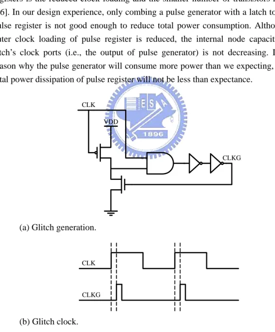
2.1.2 Pulse Registers
The idea of pulse registers is to construct a short pulse around the rising (or falling) edge of the clock as illustrated in Figure 2.3 and this pulse acts as the clock input to a latch, sampling the input only in a short window. The advantage of pulse registers is the reduced clock loading and the smaller number of transistors required [16]. In our design experience, only combing a pulse generator with a latch to form a pulse register is not good enough to reduce total power consumption. Although the outer clock loading of pulse register is reduced, the internal node capacitance of latch’s clock ports (i.e., the output of pulse generator) is not decreasing. It is the reason why the pulse generator will consume more power than we expecting, and the total power dissipation of pulse register will not be less than expectance.
VDD
CLKG CLK
(a) Glitch generation.
CLK
CLKG
(b) Glitch clock.
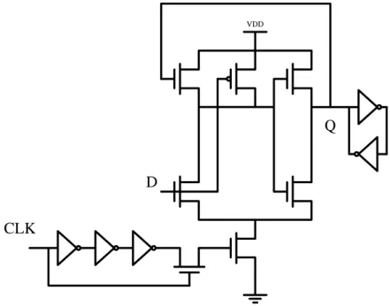
Recently, other types of pulse register called edge-triggered latch (ETL) [20] have been designed. Instead of using pulse generator, pulsed clock signals are generated in registers locally, which are used in triggering the transparent latch. The latches are transparent only during a small pulse window and they effectively act as edge-triggered flip-flop. Hybrid latch flip-flop (HLFF) is a famous one of proposed ETLs, and the pulse registers of the HLFF family shown in Figure 2.4 in [21] was discussed very well. However, in additional to their transistor numbers, sizing their transistor sizes for racing problem results in larger cell area in our experience.
VDD
D
Q
CLK
VDD
D CLK
Q
(b) Modified hybrid latch flip-flip (MHLFF).
VDD
D
CLK
Q
(c) Double-edge-triggered modified hybrid latch flip-flip (DMHLFF).
2.1.3 Sense-Amplifier-Based Registers
In a sense, the sense-amplifier-based registers illustrated in Figure 2.5 are similar in operation to the pulse registers (i.e., the first stage generates the pulse, and the second latches it). However, sense-amplifier-based registers are used extensively in memory cores and in low-swing bus drivers to sense small input signals and amplify them to generate rail-to-rail swings [16]. However, our survivor memory unit (SMU) of Viterbi decoder contains a lot of registers and multiplexers which is discussed later in detail. If the register cell is more complex and has more transistor number, the area of our SMU will be larger and not suitable for our design goal. Besides, due to the simple architecture of this register-exchange SMU, it doesn’t need to amplify signals for speeding the data rate. In [22] and [23], their complex circuit schemes and more transistor number are in the opposite direction to our expectance, so we do not discuss sense-amplifier-based registers in this SMU design.
2.1.4 Summary
There are three major types of registers: master-slave flip-flop, pulse register and sense-amplifier-based register. Master-slave flip-flops and sense-amplifier-based registers are not appropriate for register-exchange SMU designs because of their more transistor numbers and larger cell sizes. The larger cell size, the more power will be dissipated from charging and discharging the internal nodes’ capacitance. It violates our design purpose: low power high speed SMU. Although pulse registers in HLFF family should be sized very carefully for the racing problem, their smaller clock loads and less transistor numbers are very suitable for our low power high speed SMU design which is discussed in detail in Chapter 3, and the original dual-rail pulse registers’ topologies we chosen for modifying our design are introduced in the next section.
VDD VDD VDD VDD VDD VDD VDD VDD VDD D DB CLK Q QB
Figure 2.5 Illustrated sense-amplifier-based register.
2.2 Dual-Rail Pulse Registers
In this section, we focus on dual-rail pulse registers which are relative to HLFF family. We introduce two dual-rail pulse registers: dual-rail dynamic hybrid latch flip-flop [23] and dual-rail static edge-triggered latch [20]. Based on these two circuits, our modified low power static edge-triggered latch is presented in next chapter.
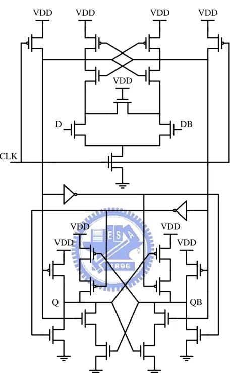
2.2.1 Dual-Rail Dynamic Hybrid Latch Flip-Flop
Figure 2.6 illustrates the dual-rail dynamic hybrid latch flip-flop (DHLFF). Referring to the figure, both DHLFF outputs are pre-discharged to the ground when the clock is low. At the rising edge of the clock and depending on the state of data at D, either Q or QB will be asserted. The outputs are held statically as long as the clock remains high. However, the pre-discharge and output-held networks increase the total cell size and the extra power dissipation.
VDD
D CLK
QB Q
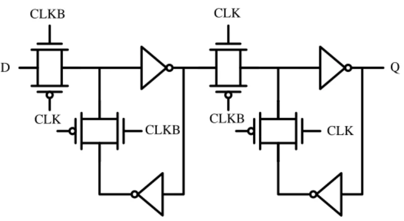
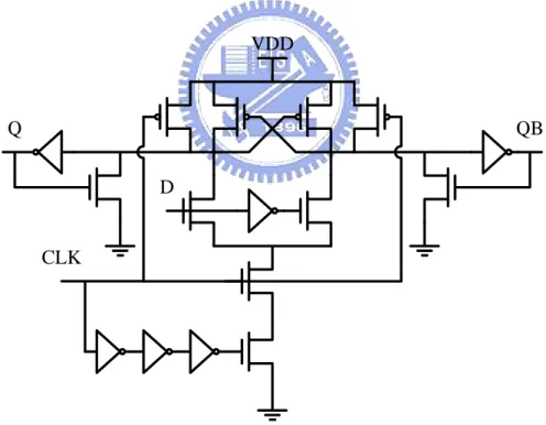
2.2.2 Dual-Rail Static Edge-Triggered Latch
The simplest type of dual-rail static edge-triggered latches (ETLs) is illustrated in Figure 2.7. It is a simplified DHLFF without the pre-discharge and output-held networks and can be viewed as a static differential cascode voltage switch (DCVS) logic latch which may switch only at the short clock pulse window. Without the pre-discharge network, it is slower than the DHLFF due to the hysteresis associated with toggling the load device [20]. However, it has less power consumption.
VDD Q D CLK QB M1 M2
Figure 2.7 Dual-rail static edge-triggered latch (ETL).
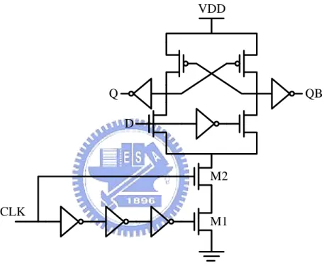
Another low power pulsed edge-triggered latch based on dual-rail static ETL is shown in Figure 2.8 and named as low swing conditional capture flip-flop [24]. It is a modified dual-rail static ETL for detecting input switching activity, and it uses NMOS transistors cascoded on the top of inverter chain to restrict voltage swing at (VDD - VT)
for saving power. By using the XOR gate to generate control signal Vg for header NMOS sleep transistor, this power gating device can save power dissipation when next input and current output being the same (i.e., switching activity is zero).
VDD VDD Q D CLK QB Vg Vg D DB QB Q Q M1 M2
Figure 2.8 Low swing conditional capture flip-flop.
Dual-rail pulse registers in this section have two benefits: less clock loads and transistor numbers which are helpful for our low power high speed SMU design. Using only two half invertors (i.e., two PMOS transistors) for keeping data is another reason of reducing power dissipation and cell size. We based on dual-rail pulse
2.3 Summary
There are three major types of registers: master-slave flip-flop, pulse register and sense-amplifier-based register. Master-slave flip-flops and sense-amplifier-based registers are not appropriate for register-exchange SMU designs because of their more transistor numbers and larger cell sizes. The larger cell size, the more power will be dissipated from charging and discharging the internal nodes’ capacitance. Although pulse registers in HLFF family should be sized very carefully for the racing problem, their smaller clock loads and less transistor numbers are very suitable for our low power high speed SMU design.
Dual-rail pulse registers maintain two benefits of pulse registers: less clock loads and transistor numbers which are helpful for our low power high speed SMU design. Otherwise, using only two PMOS transistors keeping data is another reason of reducing power dissipation and cell size. We base on this topology and propose our modified edition in Chapter 3.
Chapter 3
Design of Proposed Low Power Pulse Register
Our low power pulse registers is proposed in this chapter. The register-exchange SMU’s architecture we adopted is introduced first, and stage-reducing SMU is coming after SMU’s architecture. The design concept of our low power SMU is also pointed out here. Afterwards, the design and simulation results of our low power static edge-triggered latch based on both 0.13 um and 90 nm CMOS processes are presented. Finally, the summary is given in the end of this chapter.
3.1 Survivor Memory Unit
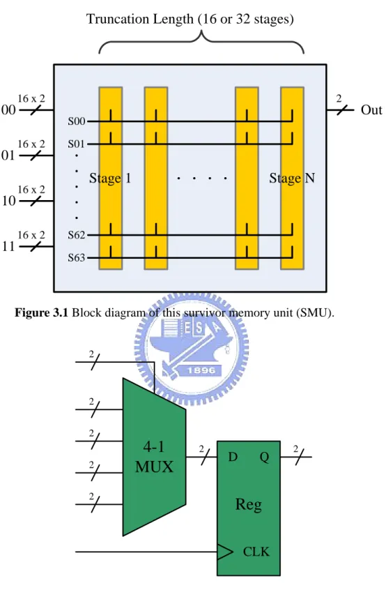
The radix-4 SMU of Viterbi decoder based on register-exchange method is illustrated in Figure 3.1. The primary inputs of this SMU are 64 2-bit constants and 64 2-bit select signals (i.e., S00 to S63) calculated from add-compare-select unit (ACSU). These 64 2-bit constants are composed of sixteen 00s, 01s, 10s and 11s of each in sequence (i.e., {16[00], 16[01], 16[10], 16[11]}). The truncation length is how many stages we use to trace the decisions to extract expected sequence, and is dependant on system specification and transmitted channel property.
In our system requirement, the truncation length is 16 or 32 for practical implementation. We use one column to represent one stage (i.e., 16 or 32 columns in our system) and each column in SMU contains 64 basic D elements as shown in Figure 3.2. Each of D elements has one 2-bit 4-to-1 multiplexer and one 2-bit register.
16 x 2 16 x 2 16 x 2 16 x 2
00
01
10
11
Truncation Length (16 or 32 stages)
S00 S01 S62 S63 2
Out
Stage 1
Stage N
Figure 3.1 Block diagram of this survivor memory unit (SMU).
4-1
MUX
Reg
D Q CLK 2 2 2 2 2 2 2Figure 3.2 Basic D element.
The interconnection information of this SMU is shown in Figure 3.3. As mentioned above, there are 64 basic D elements in one column. For example, 1_D02
1_D02’s output port is connected to the input ports of 2_D00, 2_D16, 2D_32 and 2D_48.
Alternatively, 2D_03’s four input ports are one by one linked to the output ports of
1D_12, 1D_13, 1D_14 and 1D_15. By select signals generated from the ACSU, the
4-to-1 multiplexer in the D element will choose the desired input decision passing to the output to extract targeted sequence.
00 16 32 48 00 03 01 02 04 05 06 07 08 09 10 11 12 13 14 15 00 03 01 02 00 16 32 48 00 16 32 48 00 16 32 48 04 52 20 36
1_D
001_D
011_D
021_D
031_D
162_D
002_D
012_D
022_D
032_D
163_D
003_D
013_D
023_D
033_D
16 00 16 32 48 00 03 01 02 04 05 06 07 08 09 10 11 12 13 14 15 00 03 01 02 00 16 32 48 00 16 32 48 00 16 32 48 04 52 20 363.1.1 Stage-Reduced SMU
After tracing the sequence, we found there are a relation between primary input signals and select signals as illustrated in Figure 3.4. Base on the property of primary inputs and register-exchange method, the output patterns of the first three stages are keeping in the same order despite the select signals from ACSU. Therefore we can cancel the first three stages. The select signals from ACSU become the primary inputs of stage-reducing SMU in a specified order. For example of the stage-reduced SMU in our simulation, the truncation length of 16 could be reduced to 13. It results in saving area and power proportional to reduced stages.
01 MUX 02 MUX 03 MUX 04
01 0 0 0 0 0 0 0 . . . 0 1 2 3 0 1 2 . . . 0 0 0 0 1 1 1 . . . s00 s01 s02 s03 s04 s05 s06 . . .
Could be reduced!
s00 s01 s02 s03 s04 s05 s06 . .Figure 3.4 Stage-reducing SMU.
3.1.2 Summary
Because the register-exchange based SMU contains a lot of registers and all of them need outer clock signal to work up. If we can reduce the input capacitance of clock port in registers, the clock loading of whole SMU could be scaled down and the total power consumption of the SMU could be also reduced. In the Section 2 of the Chapter 3, we will focus on which type of low power registers could have less clock loading and also less transistor number to restrict the area size of whole SMU.
transistor number, the total area of the SMU could obviously be reduced as the power consumption at the same time.
3.2 Proposed Low Swing Static Edge-Triggered Latch
In this section, we proposed our static edge-triggered latch (ETL) and the simulation results are both given here in TSMC 0.13 um and UMC 90 nm CMOS process.
As summarized in Chapter 2, dual-rail pulse registers maintain two benefits of pulse registers: less clock loads and transistor numbers which are helpful for our low power high speed SMU design. Then we focus on the dual-rail static edge-triggered latch [20], which is relative to the dual-rail dynamic HLFF in [23]. Low swing conditional capture flip-flop presented in [24] is a modified dual-rail static ETL for detecting input switching activity, and it uses NMOS transistors cascoded on the top of inverter chain to restrict voltage swing at (VDD - VT) for saving power. However,
the data switching activity in the Viterbi decoder is channel-dependent and we decide not to add conditional capture component for saving peripheral XOR gate.
3.2.1 Low Swing Static ETL in 0.13 um CMOS Process
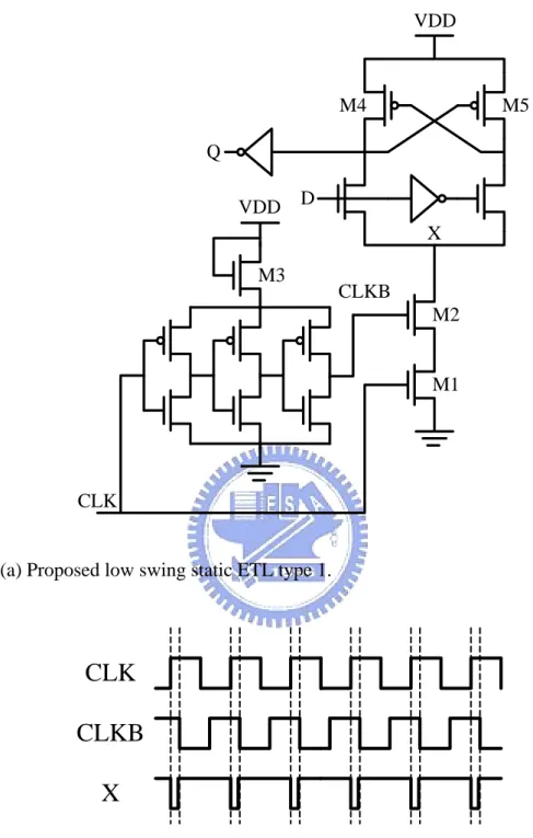
The timing information and operation principles of dual-rail pulse registers are almost the same with each other and are explained first in this section. We use our proposed low swing static ETL type 1 as an example illustrated in Figure 3.5.
The signal CLKB is inverse to the signal CLK and has a little delay time because of the inverter chain. In the usual time, the CLK and CLKB are inverse and the pull down network of the ETL turns off. Therefore, the change in input signal D will not cause any data variation in the register. When both CLK and CLKB are logic
VDD VDD Q D CLK M1 M2 M3 M4 M5 CLKB X
(a) Proposed low swing static ETL type 1.
CLK
CLKB
X
(b) Timing diagram of the low swing static ETL type 1.
Figure 3.5 Proposed low swing static ETL type 1 and its timing diagram. For reducing cell area, we use only one diode-connected NMOS M3 to limit voltage swing of the inverter chain in Figure 3.5 and also only one output buffer inverter. In the static ETL type registers, the pull down network especially M1 and
with toggling the load device (i.e., M4 and M5) and the series connection of transistors M1 and M2. Furthermore, the gate terminal of M2 is weak logic level one (VDD-VT) which results in weaker pull down driving ability of ETL. That is the reason
why we exchange the gate signals between M1 and M2 from original static ETL to our low swing static ETL for making the bottom transistor M1 have stronger driving ability.
Since we do not need the conditional capture component, we move the diode-connected NMOS M3 to the bottom of inverter chain just like footer power gating device in Figure 3.6. Therefore, both M1 and M2 have equal driving ability and pull down network is stronger than Fig. 3.5. After sizing gate width of pull down network M1 and M2 in Figure 3.6, we get smaller cell size of type 2 than type 1. Not only cell size, but also power consumption could be reduced due to smaller driving current in pull down network of our low swing static ETL type 2.
VDD VDD Q D M1 M2 M4 M5
Stronger than
type 1!
The caparison result table of registers is listed in Table 3.1. The simulation environment of this work includes the register, input signal buffer, clock buffer and output capacitance 0.7 fF for a single inverter input loading as shown in Figure 3.7. The clock frequency of all registers is at 1 GHz, and the process technology is TSMC 0.13 um CMOS logical process. The operating voltage is 1.2 V.
Table 3.1 Comparison results of different registers based on TSMC 0.13 um CMOS process. Register Type Mux-Based FF Trans-Gate FF Proposed Type 1 Proposed Type 2 Total Gate Width (um) 4.05 4.05 3.3 2.7 Clock Load (fF) 1.76 1.76 1.07 0.75 Switching Activity
IDLE 50% 100% IDLE 50% 100% IDLE 50% 100% IDLE 50% 100%
Core Power (uW) 3.00 6.93 10.82 2.98 6.36 9.70 4.11 7.18 10.10 3.68 6.42 9.12 Peripheral Power (uW) 6.35 7.82 9.33 6.21 7.79 9.36 5.75 6.89 8.09 4.84 6.06 7.28 Total Power (uW) 9.35 14.75 20.15 9.19 14.15 19.06 9.86 14.07 18.19 8.52 12.48 16.44 Average C-Q Delay (ps) 96 102.5 124 101.5 Power-Delay Product (10-15) 0.898 1.416 1.934 0.942 1.450 1.953 1.223 1.745 2.256 0.865 1.267 1.669
Input CLK_in Output 0.7 fF D Q B B CLK REG
Figure 3.7 The simulation environment of this work.
As mentioned in Table 3.1, the total power is the sum of the core power and the peripheral power. The peripheral power which is the power dissipated by input and clock buffers and the output loading is used here to stand for especially showing the importance of reducing system clock load. Because of the stacking effect, the transmission-gate flip-flop (TGFF) has the least core power when data switching activity being not so high. However, TGFF’s total gate width and clock load are equal to the multiplexer-based flip-flop (MBFF) that results in large area and peripheral power despite its lower core power.
Our proposed type 1 low swing static edge-triggered latch (ETL) proves the benefit of reduced clock load in the peripheral power term. However, due to sizing the pull down network of the proposed type 1 latch for the hysteresis of the pull up network, our type 1 latch consumes greatest core power when data switching activity being low. In addition, the proposed type 1 latch has the greatest average C-Q delay.
After changing the diode-connected NMOS to the bottom of the delay chain as the footer power gating device, the transistor sizes of M1 and M2 in Figure 3.6 could be scaled down. Thus, the clock load of our type 2 low swing static ETL is the least
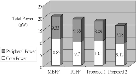
Vertical stacked bar charts of different registers’ power consumption data in 0.13 um CMOS process of different switching activities are given in Figure 3.8 as a short summary. It is clear that our low swing static latch has lower power consumption. 3 6.35 2.98 6.21 4.11 5.75 3.68 4.84 0 1 2 3 4 5 6 7 8 9 10 Total Power (uW) MBFF TGFF Proposed 1 Proposed 2 Peripheral Power Core Power
(a) Switching activity is IDLE.
6.93 7.82 6.36 7.79 7.18 6.89 6.42 6.06 0 2 4 6 8 10 12 14 16 Total Power (uW) MBFF TGFF Proposed 1 Proposed 2 Peripheral Power Core Power (b) Switching activity is 50 %.
10.82 9.33 9.7 9.36 10.1 8.09 9.12 7.28 0 5 10 15 20 25 Total Power (uW) MBFF TGFF Proposed 1 Proposed 2 Peripheral Power Core Power (c) Switching activity is 100 %.
Figure 3.8 Vertical stacked bar charts of different switching activities in 0.13 um CMOS process.
3.2.2 Low Swing Static ETL in 90 nm CMOS Process
The comparison table based on 90 nm CMOS process is given in Table 3.2. In this 90 nm CMOS process simulation condition, we do not considerate our proposed type 1 low swing static ETL as a beta edition in Section 3.2.1. Otherwise, the simulation environment is the same as illustrated in Figure 3.7. The clock frequency of all registers is at 1 GHz, and the process technology is UMC 90 nm CMOS logic and mixed-mode 1.0V standard performance process.
Table 3.2 Comparison results of different registers based on UMC 90 nm CMOS process. Register Type Mux-Based FF Trans-Gate FF Proposed Type 2 Total Gate Width (um) 3.24 3.24 2.16 Clock Load (fF) 1.17 1.17 0.57 Switching Activity
IDLE 50% 100% IDLE 50% 100% IDLE 50% 100%
Core Power (uW) 1.75 4.02 6.26 1.75 3.78 5.76 2.43 4.08 5.71 Peripheral Power (uW) 3.50 4.49 5.50 3.49 4.50 5.51 2.92 3.55 4.20 Total Power (uW) 5.25 8.51 11.76 5.24 8.28 11.27 5.35 7.63 9.91 Average C-Q Delay (ps) 52.5 53.7 40.1 Power-Delay Product (10-15) 0.276 0.447 0.617 0.281 0.445 0.605 0.215 0.305 0.397
Unlike the trend of simulation results in 0.13 um CMOS process, our low swing static ETL has the smallest average C-Q delay to all of the above registers. Although our design still has the smallest cell size and the least clock load, its core power is grater than other two master-slave flip-flops. Because of the always turn-on diode- connected NMOS M3 in the bottom of delay chain in Figure 3.6 and the always turn-on pull up networks (i.e., the hysteresis of dual-rail topology), the leakage power consumption becomes a major problem of our design. Vertical stacked bar chart of all the above comparisons are given in Figure 3.9 as a sort summary. It is obvious that our low swing static ETL in 90 nm CMOS process has to deal with static leakage power consumption when switching activity is idle.
1.75 3.5 1.75 3.49 2.43 2.92 0 1 2 3 4 5 6 Total Power (uW) MBFF TGFF Proposed 2 Peripheral Power Core Power
(a) Switching activity is IDLE.
4.02 4.09 3.78 4.5 4.08 3.55 0 1 2 3 4 5 6 7 8 9 Total Power (uW) MBFF TGFF Proposed 2 Peripheral Power Core Power
6.26 5.5 5.76 5.51 5.71 4.2 0 2 4 6 8 10 12 Total Power (uW) MBFF TGFF Proposed 2 Peripheral Power Core Power (c) Switching activity is 100 %.
Figure 3.9 Vertical stacked bar charts of different switching activities in 90 nm CMOS process.
Next, we simulated our low swing static ETL in UMC 90 nm CMOS logic and mixed-mode 1.2 V low leakage with high threshold voltage process. The operating voltages are 1.2 V and 1.0 V, but other simulation conditions are all the same with the above. As listed in Table 3.3, with low leakage devices the core power decreased. But the legal operating voltage of the low leakage process is 1.2 V, according to the Formula 2.1 in Chapter 2, it resulted in more power dissipation when the switching activity going to be high. Then we reduced the operating voltage from 1.2 V to 1.0 V for saving peripheral power dissipation, and we get lower power consumption data.
However, the total power consumption and static leakage power dissipation could be reduced by means of low leakage process; it is noticeable that the speeds of circuits degenerate very much as shown in Table 3.3. The power-delay products in low leakage process are much larger than in standard process due to the performance degeneration. Vertical stacked bar charts of power consumption in different switching activities are given in the end of Section 3.2.3 with other low leakage technique as a short summary.
Table 3.3 Comparison results of proposed design in different 90 nm CMOS processes Process Type Standard Performance Low Leakage in 1.2 V Low Leakage in 1.0 V Total Gate Width (um) 2.16 2.16 2.38 Clock Load (fF) 0.57 0.49 0.56 Switching Activity
IDLE IDLE IDLE IDLE 50% 100% IDLE 50% 100%
Core Power (uW) 2.43 4.08 5.71 0.51 3.85 7.00 0.07 3.24 6.20 Peripheral Power (uW) 2.92 3.55 4.20 3.39 4.25 5.20 2.50 3.23 3.67 Total Power (uW) 5.35 7.63 9.91 3.90 8.10 12.20 2.57 6.47 9.87 Average C-Q Delay (ps) 40.1 159.0 319.5 Power-Delay Product (10-15) 0.215 0.305 0.397 0.620 1.288 1.940 0.821 2.067 3.153
3.2.3 Low Swing Static ETL in 90 nm MTCMOS Process
high VT transistor is used in the non-critical path to reduce the leakage current. The
MTCMOS technique is used to reduce the static power with no overhead in the performance.
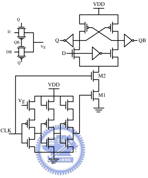
After utilizing MTCMOS technique, our low swing static ETL is illustrated in Figure 3.10. We use the low threshold voltage device in the critical path to increase the operation speed, and use the high threshold voltage device in the non-critical path and leakage path to reduce both the dynamic power and static power consumption. According to the design issues, the pull up network (i.e., the pre-charged PMOS transistor pair), M4 and M5, diode-connected NMOS M3, and the delay chain are used the high VT device to reduce the leakage power as shown in Figure 3.10. In our
design experience, the pull down network of our design could not be replaced by high VT device because the diving ability will degenerate and it will result in error
operation. VDD Q D CLK M1 M2 M3 M4 M5 High VT Device
Figure 3.10 Proposed low swing static ETL in MTCMOS.
The comparison table based on UMC 90 nm CMOS logic and mixed-mode 1.0V standard performance process with and without MTCMOS technique is given in
3.7. The clock frequency of all registers is at 1 GHz.
As shown in Table 3.4 in Page 36, the low swing static ETL with MTCMOS technique has all advantages to non-MTCMOS low swing static ETL in every compared term. After using MTCMOS technique to replace the delay chain and the pull up network, the core power consumption is extra low than before. Especially in average C-Q delay, due to the weaker pull up network, M4 and M5, the pull down network is much easier to resist the hysteresis of dual-rail topology. Therefore, the low swing static ETL with MTCMOS is faster than it without MTCMOS and it brings about the incredible small power-delay product.
Table 3.4 Comparison results of proposed Design with and without MTCMOS technique in 90 nm CMOC process.
Process Type Without MTCMOS With MTCMOS Total Gate Width (um) 2.16 2.16 Clock Load (fF) 0.57 0.53 Switching Activity IDLE 50% 100% IDLE 50% 100% Core Power (uW) 2.43 4.08 5.71 0.12 1.45 2.79 Peripheral Power (uW) 2.92 3.55 4.20 2.87 3.55 4.21 Total Power (uW) 5.35 7.63 9.91 2.99 5.00 7.00
Vertical stacked bar charts of different registers’ power consumption data in 90 nm CMOS low leakage and MTCMOS processes of different switching activities are given in Figure 3.11 as a short summary. It is apparent that our low swing static latch with MTCMOS technique has lower power consumption except for idle condition.
2.43 2.92 0.51 3.39 0.07 2.5 0.12 2.87 0 1 2 3 4 5 6 Total Power (uW) Standard Process Low Leakage in 1.2 V Low Leakage in 1.0 V With MTCMOS Peripheral Power Core Power
(c) Switching activity is IDLE.
4.08 3.55 3.85 4.25 3.24 3.23 1.45 3.55 0 1 2 3 4 5 6 7 8 9 Total Power (uW) Standard Process Low Leakage in 1.2 V Low Leakage in 1.0 V With MTCMOS Peripheral Power Core Power (c) Switching activity is 50 %.
5.71 4.2 7 5.2 6.2 3.67 2.79 4.21 0 2 4 6 8 10 12 14 Total Power (uW) Standard Process Low Leakage in 1.2 V Low Leakage in 1.0 V With MTCMOS Peripheral Power Core Power (c) Switching activity is 100 %.
Figure 3.11 Vertical stacked bar charts of different switching activities in 90 nm CMOS low leakage and MTCMOS processes.
In this section, we introduce our modified dual-rail static ETL named low swing static ETL. Based on simulating in both 0.13 um CMOS process and 90 nm CMOS process, our design has the lowest total power consumption and peripheral power dissipation, the smallest cell size and clock load and the incredible small power-delay product especially in 90 nm CMOS process with MTCMOS technique. The smaller cell size and less clock load are suitable for our register-exchange SMU design and we base on our low swing static ETL to build the low power high speed SMU of Viterbi decoder in Chapter 4.
3.3 Summary
In Chapter 3, we began with introducing the architecture of our register- exchange SMU of Viterbi decoder. Because the register-exchange based SMU contains a lot of registers and all of them need outer clock signal to stimulus. If we can reduce the input capacitance of clock port in registers, the clock loading of whole SMU could be scaled down and the total power consumption of the SMU could be also reduced. Otherwise, because this SMU contains a lot of registers, if we can have registers with less transistor number, the total area of the SMU could obviously be reduced as the power consumption at the same time. Therefore, pulse registers which have two benefits: less clock loads and transistor numbers become our design choice of registers.
Next, we propose our modified dual-rail static ETL named low swing static ETL. According to the simulation results in 0.13 um CMOS process and 90 nm CMOS process, our low swing static ETL has the lowest total power consumption and peripheral power dissipation, the smallest cell size and clock load and the incredible small power-delay product especially in 90 nm CMOS process with MTCMOS technique. We will base on our low swing static ETL to construct the low power high speed SMU of Viterbi decoder in Chapter 4.
Chapter 4
Implementation of Proposed Survivor Memory Unit
The physical implementation description and post-layout simulation results of our proposed survivor memory unit are presented in this chapter. We first begin with detailed architecture of our register-exchange based SMU design in Section 4.1. The floorplan and clock tree network design of proposed SMU are also given in this section. Next, Section 4.2 demonstrates our fully custom layouts of basic cells and the whole SMU block. Afterwards, the comparison results between pre-layout simulation and post-layout simulation are available in the end of this chapter. These post-layout simulation results are based on TSMC 0.13 um CMOS technology.
4.1 Architecture of Proposed Survivor Memory Unit
In this section, first we introduce the detailed architecture of our proposed radix-4 SMU in Figure 4.1. Although the non stage-reduced register-exchange SMU with 16 stages is enough to trace the expected sequence in general case, we use 32 stages’ architecture for more accuracy in physical implementation. After using stage-reducing technique as mentioned in Chapter 3, the basic architecture of our SMU design has 29 stages (i.e., stage 00 to stage 28) as in Figure 4.1. The primary input d0 to d63 are 64 2-bit select signals from add-compare-select unit (ACSU), and the interconnection information between each stage is the same as described in Chapter 3.
d0 d1 d62 d63 D00_0 D28_63 D00_1 D00_62 D00_63 D01_0 D01_1 D01_62 D01_63 D02_0 D02_1 D02_62 D02_63 D28_0 D28_1 D28_62 0 1 2 3 4 5 6 7 60 61 62 63 56 57 58 59 15 31 47 63 15 31 47 63 0 16 32 48 0 16 32 48 0 1 2 3 4 5 6 7 60 61 62 63 56 57 58 59 15 31 47 63 15 31 47 63 0 16 32 48 0 16 32 48 0 1 2 3 4 5 6 7 60 61 62 63 56 57 58 59 15 31 47 63 15 31 47 63 0 16 32 48 0 16 32 48 2 2 2 2 OUT
Figure 4.1 Basic architecture of proposed SMU.
4.1.1 Floorplan and Folded Last Three Stages’ SMU
The floorplan of this proposed SMU is shown in Figure 4.2. In our radix-4 architecture of SMU, the data are all 2-bit signals. For reducing the complexity of metal line interconnection between each stages of SMU for physical route, we divide whole memory core into two parts as shown in Figure 4.2. Each 1-bit SMU block handles 1-bit input signal and combining these two blocks’ output we can get desired 2-bit output data. Then we set the clock buffer in the middle of the floorplan to separate those two 1-bit SMU blocks. Because the clock network of a memory module is very important in VLSI design, according to this floorplan, the clock network of proposed SMU could distribute the clock signal to each stage in SMU evenly. The detailed clock network design of proposed SMU is described in next sub-section later. Finally, the input buffers are set to the right side of the floorplan as common seen and the output buffers are included in those two 1-bit SMU blocks.
1-bit SMU
1-bit SMU
Input
Buf
fer
Clock Buffer
Input
Buffer
CLK
Inputs [0]
Inputs [1]
64 64Figure 4.2 The floorplan of proposed SMU.
As shown in Figure 4.1, the primary output port of our SMU is the output of the first D element in the last stages (i.e., stage 28). It is obvious that other 63 D elements from D28_1 to D28_63 can be eliminate from our SMU block in physical implementation. Due to the interconnection information mentioned in Chapter 3, not only the last stages has redundant D elements could be removed, but also the stage 27 and stage 26 have redundant D elements could be eliminated in physical design.
The detailed D elements-saving in last 3 stages is illustrated in Figure 4.3. Besides the stage 28 only needs one D element, the stage 27 needs four D elements and stage 26 needs sixteen ones. In this rectangle figure, the bottom part of stage 26, stage 27 and stage 28 shows a lot of area could be saved in physical implementation if we can integrate the last three stages 26, 27 and 28 in one physical column domain. We call this concept “Folded Last Three Stages’ SMU,” and the physical layout of the folded last three stages’ SMU is given in the Section 4.2.1.
Area could be saved!
16D 4D 1D 64DStage
25
Stage
26
Stage
27
Stage
28
Figure 4.3 The D elements-saving in last 3 stages.
4.1.2 Clock Tree Network Design
The clock network with fan-out information of this work is illustrated in Figure 4.4. After calculating load capacitance, the pre-buffer of clock signal is an inverter chain composed of four inverters which are 1 : 1 : 4 : 16 in aspect ratios. The outputs of pre-buffer are connected to twenty six stage-buffers for stage 00 to stage 25 and the folded last three stage (i.e., stage 26, 27 and 28). Each stage-buffer in Figure 4.4 is composed of four inverters which are 1 : 4 : 16 : 64 in aspect ratios for driving each stage. As mentioned in Section 4.1.1 we setting the clock buffer in the middle of the floorplan to distribute the clock signal in SMU evenly, the local detailed block diagram of clock tree network is shown in Figure 4.5 as reference to Figure 4.2. The most interesting thing is that the clock tree network is fed with the clock signal from the right side of the floorplan as shown in Figure 4.2 which does not usually occur as input signals. The reason why we feeding the clock tree network by this way is making sure to avoid positive clock skew in our SMU design. Because the register-exchange based SMU acts like a lot of shift registers with multiplexers, the delay between two registers (i.e., the delay of the multiplexer) is too small to keep away from hold time violation. If we feed the clock tree network from the right side of the network, the negative clock skew to the whole clock tree network is helpful for avoiding hold time violation in physical implementation.
Last Three Stages (26, 27 and 28) Stages 25 Stages 24 Stages 00 CLK Pre-Buffer 1 : 1 : 4 : 16 Stage-Buffer 1 : 4 : 16 : 64
Figure 4.4 Illustrated clock tree network.
Pre-Buffer Buffer of Stage 25 Buffer of Stage 24 Buffer 0f Stage 0 CLK Upper Stage 00 Upper Stage 24 Upper Stage 25 Upper Last Three Stages
4.1.3 Design Flow
In order to accomplish the implementation of proposed SMU design especially focusing on low power and small area specifications, we choose our low power low swing static edge-triggered latch (ETL) as a basic register cell which is different to traditional master-slave flip-flops using in today’s cell-based design flow. With the purpose of integrating our proposed low swing static ETL in this SMU design, we decide to take the fully custom solution to implement this hard memory macro. The design flow of this work is described in this sub-section and illustrated in Figure 4.6.
According to the architecture conforming to the specification, we first establish the netlist file of proposed SMU design in Hspice format in order to run pre-layout simulation by means of Synopsys Hspice simulator. After making sure there being no time violation and the function of proposed SMU being correct, we start to convert the schematic of this design to physical layout by using layout editor Cadence Virtuoso. When finish the layout of this work, there are three major steps need to be done before running the post-layout simulation. The first two steps of above are usually regarded as post-layout verification steps. One is the design rule check (DRC), and the other is the layout versus schematic (LVS). DRC checks the data of physical layouts against the design rules of fabrication, because manufacturing processes have inherent limitations in accuracy and the design rule documents specify geometry of masks which will provide reasonable yields. LVS checks the identity of physical layouts to its relative schematic netlist files. As shown in Figure 4.6, after DRC checking, we use the original Hspice netlist to campare with the physical layout information from Virtuoso in LVS step. There might be a lot of iterations to fix the physical layouts to obey the DRC documents and to match the original netlists if there is any error in these two post-layout verification steps. After confirming the identity of netlists and physical layouts, we then start to run the step of layout parameter extraction (LPE) preparing for post-layout simulation. LPE can extract layout parameters including parameters of transistors, parasitic capacitors and resistors, and the extracted netlist could be used in post-layout transistor-level simulation. All of above these three steps, DRC, LVS and LPE, could be completed by the aid of Mentor Calibre. Finally we get the extracted netlist file after LPE, and then we can run the post-layout simulation in Synopsys Nanosim environment as a fast Spice simulator especially suitable for digital VLSI design.
Hspice
Virtuoso
Calibre
Calibre
Calibre
Nanosim
Pre-Layout
Simulation
Layout Editor
Design Rule
Check (DRC)
Layout Versus
Schematic (LVS)
Layout Parameter
Extraction (LPE)
Post-layout
Simulation
Netlist
Architecture
Design
4.2 Implementation Results
In this section, fully custom physical layouts of this work are introduced first. Not only the basic D element’s layout is demonstrated, but also the whole SMU block’s layout is shown later. The post-layout simulation results calculated from Synopsys Nanosim simulator are given and also compared with the pre-layout simulation data in Section 4.2.2. In this section, all the physical implementations are based on TSMC 0.13 um CMOS technology.
4.2.1 Physical Layout Descriptions
The physical layouts of proposed low swing static ETL and the 4-to-1 multiplexer is shown in Figure 4.7. The standard cell sizes of each one are the same because of their similar transistor numbers and the convenience for integrating. The height of the standard cell is about 4 um and the width is about 10 um.
(b) The layout of the 4-to-1 multiplexer (4 * 10 um2).
Figure 4.7 The layouts of low swing static ETL and 4-to-1 multiplexer.
The layout of the basic D element given in Figure 4.8 is 4*20 um2 in dimension and it is obvious that the height of the standard cell is restricted by the 4-to-1 multiplexer’s four input ports. That is why the area utilization of our low swing static ETL is not as small as possible. The Figure 4.9 shows the layout of partial one stage constructed of 64 basic D elements. The interconnection routing between each stage is illustrated in Figure 4.10. Because the interconnection is complex due to a lot of input ports of each basic D element, the area for interconnection routing dominates the
partial clock tree network is illustrated in Figure 4.14 as referenced to Figure 4.5, and the layout of wire-group power rings for distributing supply current evenly in whole hard macro in this design is demonstrated in Figure 4.15.
Figure 4.12 The layout of the whole SMU block (450 * 1540 um2) as referenced to the floorplan in Figure 4.2.
Figure 4.14 The partial clock tree network of this work including pre-buffer and last five stage-buffers as referenced to Figure 4.5.
4.2.2 Post-Layout Simulation Results
Before we show the post-layout simulation result of this SMU hard macro, we give the post-layout simulation result of proposed low swing static ETL compared with the pre-layout simulation result in Chapter 3 first. After Calibre LPE extraction, the post-layout simulation shows the degeneration as compared with the pre-layout simulation in power and speed domain due to the parasitic capacitors and resistors in physical layout. The Table 4.1 shows the comparison results of pre-layout and post-layout simulations. The peripheral powers in these two conditions are almost the same, but the core power of post-layout simulation is slightly higher than pre-layout simulation. The average C-Q delay has the same situation in this comparison, and they result in larger power-delay product in post-layout simulation.
Table 4.1 Simulation results of proposed low swing static ETL in pre-layout simulation and post-layout simulation.
Simulation Type Pre-Layout Simulation Post-Layout Simulation Total Gate Width (um) 2.7 2.7 Clock Load (fF) 0.75 0.748 Switching Activity
IDLE IDLE IDLE IDLE 50% 100%
Core Power (uW) 3.68 6.42 9.12 4.41 8.14 11.80 Peripheral Power (uW) 4.84 6.06 7.28 4.93 6.10 7.30 Total Power (uW) 8.52 12.48 16.44 9.34 14.24 19.10 Average C-Q Delay (ps) 101.5 104.8 Power-Delay Product (10-15) 0.865 1.267 1.669 0.979 1.492 2.002
Because in whole SMU block pre-layout simulation we use only 16 and 13 stages to verify the functionality for reducing simulation complexity, so we first show the 13 stages SMU post-layout simulation results for comparing in Table 4.2. After stage-reducing, the pre-layout simulation result of 13 stages SMU block has lower power consumption than 16 stages SMU and the saved power is proportional to stages which are removed. In post-layout simulation result, we can see that the power consumption is about 2 mW higher than pre-layout simulation due to the parasitic capacitors and resistors in the layout. Besides, in this comparison we only focus on the functionality is correct or not. The simulation circuit includes only SMU core without I/O buffers and the clock tree network. We will show the post-layout simulation results of whole 29 stages SMU block (i.e., 32 stages after stage-reducing) with I/O buffers and the clock tree network later in implementation for practical applications.
Table 4.2 Simulation results of the 16 and 13 stages SMU block in pre-layout simulation and post-layout simulation.
Simulation Target 16 Stages SMU Block 13 Stages SMU Block Simulation Type Pre-Layout Simulation Pre-Layout Simulation Post-Layout Simulation Operation Voltage 1.2 V 1.2 V 1.2 V Clock Frequency 1 GHz 1 GHz 1 GHz Power Consumption 15.26 mW 13.53 mW 15.42 mW
Table 4.3 Simulation results of the 29 stages SMU block with and without I/O buffers and clock tree network in post-layout simulation.
Simulation Target
29 Stages SMU Block without I/O Buffers and
Clock Tree Network
29 Stages SMU Block with I/O Buffers and Clock Tree Network
Simulation
Type Post-Layout Simulation
Operation Voltage 1.2 V 1.2 V Clock Frequency 1 GHz 1 GHz Power Consumption 31.28 mW 41.10 mW
The comparison result between SMU designs in cell-based design flow and fully custom design flow is given in Table 4.4, and in this operation condition the operating frequency 250 MHz is fast enough to meet our system specification. The power consumption of the SMU synthesized from EDA tool is 37.61 mW, and our fully custom SMU hard macro consumes only 10.28 mW under the equal test pattern. Our fully custom SMU hard macro’s power consumption is merely about 27.3% when compared to the power consumption of the synthesized SMU.
Table 4.4 Simulation results of the 29 stages SMU block from EDA synthesis tool and this work in post-layout simulation.
Simulation Target
29 Stages SMU from EDA Synthesis Tool
Fully Custom 29 Stages SMU Hard Macro
Simulation
Type Post-Layout Simulation
Operation Voltage 1.2 V 1.2 V Clock Frequency 250 MHz 250 MHz Power Consumption 37.61 mW 10.28 mW
According to Equation 2.1 in Chapter 2, the most direct way for reducing dynamic power is lowering the operating voltage because of its square property. In our SMU design we have our own local power ring and it is convenient if we can implement our Viterbi decoder in multi-level voltage environment such like the voltage islands in [25-27], the operating voltage of this SMU hard macro could decrease and so as the power consumption. Table 4.5 shows the simulation result after lowering the operating voltage to 1.0 V, the power consumption of this work is 6.63 mW in 0.13 um CMOS process. It evidences that reducing supply voltage level is powerful in low power applications and the reduced part of power consumption is almost proportional to the calculated answer by using Equation 2.1.
Table 4.5 Simulation results of this SMU hard macro in different operating voltages for reducing power consumption.
Simulation
Target Fully Custom 29 Stages SMU Hard Macro Simulation
Type Post-Layout Simulation
Operation Voltage 1.2 V 1.0 V Clock Frequency 250 MHz 250 MHz Power Consumption 10.28 mW 6.63 mW
In the end of this section, we compare the power data of this work with recent Viterbi decoders. After gate-level simulating of other Viterbi decoder’s components, the power consumption of transition metric unit (TMU) and add-compare-select unit
Table 4.6 Comparison of this work with recent Viterbi decoders.
Process Operating
Voltage Power @ Performance
This Work 0.13 um CMOS 1.2 V 67
.
86 mW @ 500 Mb/s 1.2 V 970 mW @ 2 Gb/s [17] 0.13 um CMOS 1.5 V 2200 mW @ 2.8 Gb/s 0.7 V 5 mW @ 54 Mb/s [18] 90 nm CMOS 1.2 V 40 mW @ 500 Mb/s4.3 Summary
In the beginning of Chapter 4, we start at describing the architecture of our proposed SMU clearly. We adopt the 29 stages register-exchange based SMU architecture as our design for real implementation after stage-reducing. In our 2-bit radix-4 SMU floorplan, for reducing the interconnection complexity in local routing we split this 2-bit SMU core into two parts in physical implementation and each part deals with 1-bit signals. From calculating node capacitances, we design the appropriate clock tree network including clock buffers carefully. Also for distributing the clock signal evenly in this design, we insert the clock tree network between these two 1-bit SMU cores in floorplan. And we introduced the concept “the folded last three stages’ SMU” for saving area of redundant basic D elements in last three stages in this SMU design. In the end of Section 4.1 are the fully custom design flow and the relative EDA tools used in this work.
In the second part in Chapter 4, we demonstrate several fully custom layouts including basic cells and the completed SMU block used in this work. After post-layout simulation, the proposed completed SMU hard macro in our specified test patterns consumes 41.10 mW at 1 GHz clock rate and the operating voltage is 1.2 V. The area of this work is 570 * 1660 um2, and these power and area data are very outstanding as reference to synthesized SMU designs from cell-based design flow. Then, the concept of “Voltage islands” is used to reduce total power consumption of the whole Viterbi decoder. After lowering the operating voltage to 1.0 V, the power consumption of this work is 6.63 mW at 250 MHz under the same test pattern. The comparison of this work with recent Viterbi decoders is in the end of this chapter.