行政院國家科學委員會專題研究計畫 成果報告
子計畫一:碳基奈米結構材料之製程及其在場效發射顯示上
之應用(3/3)
計畫類別: 整合型計畫 計畫編號: NSC93-2216-E-009-004- 執行期間: 93 年 08 月 01 日至 94 年 10 月 31 日 執行單位: 國立交通大學材料科學與工程學系(所) 計畫主持人: 郭正次 報告類型: 完整報告 處理方式: 本計畫可公開查詢中 華 民 國 94 年 7 月 25 日
行政院國家科學委員會補助專題研究計畫成果報告
※※※※※※※※※※※※※※※※※※※※※※※※
※
※
※ 光資訊關鍵性材料製程與性質研究-總計畫(3/3) ※
※
※
※※※※※※※※※※※※※※※※※※※※※※※※
計畫類別:□個別型計畫 ■整合型計畫
計畫編號:
NSC92-2216-E-009-009
執行期間:2004 年 8 月 1 日至 2005 年 7 月 31 日
主持人:郭正次
國立交通大學 材料科學與工程學系
共同
主持人:張立 謝宗雍 陳三元 吳耀銓 陳家富
計畫參與人員:
本成果報告包括以下應繳交之附件:
□赴國外出差或研習心得報告一份
□赴大陸地區出差或研習心得報告一份
□出席國際學術會議心得報告及發表之論文各一份
□國際合作研究計畫國外研究報告書一份
執行單位:國立交通大學 材料科學與工程學系、機械工程學系
中 華 民 國 94 年 5 月 31 日
行政院國家科學委員會專題研究計畫期中進度報告
光資訊關鍵性材料製程與性質研究-總計畫(3/3)
執行期限:93 年 8 月 1 日至 94 年 7 月 31 日
計畫編號:
NSC92-2216-E-009-009
主持人:郭正次
國立交通大學 材料科學與工程學系
共同
主持人:張立 謝宗雍 陳三元 吳耀銓 陳家富
子計畫一:
碳基奈米結構材料之製程及其在場效顯示器上之應用
計畫編號:
NSC92-2216-E-009-010
主持人:郭正次
國立交通大學 材料科學與工程學系
摘要 本研究藉由為了操控碳奈米結構及其 場發射性質,利用 H2、NH3、Ar、C2H2 和 CH4 氣體源以微波電漿化學氣相沉積法 進行碳奈米管及碳奈米尖錐的合成。碳奈 米 結 構 藉 由 改 變 下 列 的 製 程 參 數 來 操 控:氣體源的成分、基材偏壓、沉積時間、 基材溫度、電漿前處理和電漿後處理。所 合成的產物為碳奈米管或是碳奈米尖錐 主要取決於基材溫度和負偏壓的施加。在 場發射性質方面,由於碳奈米尖錐有較大 的場發射增強因子因而顯現出比碳奈米 管優良的性質。準直碳奈米管在無偏壓輔 助成長 10 分鐘且沒有經過後處理的場發 射性質表現最好,其開啟電場 (Eto) ~ 4.4 V/m; 起始電場 (Eth) ~ 8.26 V/m;場發射 增強因子β ~ 4096,而在 10 V/m 的電場下 可達 88.7 mA/cm2。另外在-300 V 偏壓輔 助 下 成 長 準 直 碳 奈 米 尖 錐 之 開 啟 電 場 (Eto) ~ 5.0 V/m;起始電場 (Eth) ~ 6.99 V/m;場發射增強因子β ~ ?4993,而在 10 V/m 的電場下更可達 173.42 mA/cm2,而 且碳奈米尖錐對基材的附著性比碳奈米 管更為優異。
關鍵詞:微波電漿化學氣相沉積法、場發 射、奈米管、碳奈米尖錐 AbstractIn order to develop and investigate the critical materials applied in field emission (FE) display, carbon nanotubes (CNTs) and carbon nanocones (CNCs) could be synthesized by microwave plasma chemical vapor deposition (MPCVD) method with H2,
NH3, Ar, C2H2 and CH4 as plasma sources.
Therefore, the carbon-like nanostructures and their properties were manipulated by varying several process parameters, such as atmosphere composition, substrate bias, deposition time, substrate temperature, and plasma treatments; where the substrate temperature and the applied negative bias are the mostly important factors to synthesize CNTs or CNCs. The morphologies and nanostructures of the CNTs and CNCs are characterized by field emission scanning electron microscopy (FESEM) and high resolution transmission microscopy (HRTEM) respectively. In terms of FE properties, the CNCs are expected own better emission properties than CNTs due to the greater enhancement factor. Thus, the FE characteristics of the as-grown well-aligned CNTs demonstrate the well properties of Eto ~ 4.4 V/µm, Eth ~
8.26 V/µm, field enhancement factor
β ∼ ?4096, and J ~ 88.7 mA/cm2 at 10 V/µm. Moreover, the high area density and uniformity of CNCs exhibit the better results of Eto ~ 5.0 V/µm, Eth ~ 6.99 V/µm,
173.42 mA/cm2 at 10 V/µm.
Keywords: microwave plasma chemical vapor deposition (MPCVD), carbon nanotubes (CNTs), carbon nanocones (CNCs)
2. Introduction
Recently carbon nanotubes (CNTs) [1] and carbon nanocones (CNCs) [2-4] are gained a greater attention in application of field emission (FE) devices due to their morphologies with high aspect ratio in nanoscale. In order to obtain the practical application of FE devices, how to manipulate the nanofabrication of carbon nanostructure and their FE properties are important topics needed to study and develop. According to the literature reviews, the field emission properties of these carbon nanostructures are affected by their tube diameters, orientation, morphologies, bonding structure, number density and adhesion between the substrate. Here the microwave plasma chemical vapor deposition (MPCVD) system is employed to synthesize carbon nanostructures in this experiment. All the effect factors of field emission for carbon nanostructures are corresponding to the deposited process parameters such as plasma pretreatment, species of precursor gases, precursor gases ratio, bias applied, deposition time and deposition temperature. Hence, by manipulating process parameters on MPCVD method to synthesize high aspect ratio, carbon-based nanostructures for gaining better FE properties are the purposes of experimental motivation.
3. Results and Discussion
3.1 The morphologies of CNTs
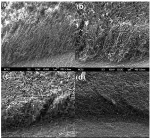
To obtain well-aligned CNTs as well field emitters, various negative substrate bias are operated in the process and the morphologies of the CNTs are shown in
Figs. 1(a) ~ (d). It shows a greater negative applied bias is the favor condition to grow CNTs with well alignment, though the tube number density, length, and diameter of CNTs are no significant differences among these results. It is interesting to note that the IG/ID ratios for these specimens are from
0.98 to 1.02 by increasing the applied substrate bias from -50 to -250 V. The reasons for higher IG peak at higher negative
applied bias may relate to greater ions bombardment energy at higher applied potential which could be able to clean the carbonaceous defects on the structure surface and to maintain the carbon diffusion path to form graphitized CNTs. Furthermore, the negative substrate bias can enhance the potential of the plasma sheath, which is a zone among of the plasma and substrate surface owned negative potential. In the sheath, electrons may be rejected, but the positive ions can be concentrated and obtained to bombard the substrate as the accelerated ions. Well- aligned CNTs would be formed by the oriented plasma ions assisted with applied electric field. By contrast, the wave-like CNTs can be considered have more defect than aligned CNTs due to existence of more pentagonal and heptagonal rings [5].
3.2 Field emission properties of the well-aligned CNTs
The results of CNTs FE properties, which with or without applied bias assisted growth, indicate that the as-grown CNTs without applied bias has the best FE properties, where Eto and Eth are ~ 4.4 V/µm
and ~ 8.26 V/µm, respectively, the current density at 10V/µm is ~ 88.7 mA/cm2, field enhancement factor β ~ 4096 as shown in Fig. 6. However, about the stability of the as-grown CNTs show that the most of the CNTs were damaged or stripped off from the substrate by an electric field of 10 V/µm after repeated measurements for less than ten times. The reason may be due to weak bonding between the substrate and the
CNTs which lead CNTs stripping and damage during the repeated applications of electric field.
3.3 Effects of applied bias and H2 / CH4
ratio on CNCs growth
Under the same H2/CH4 ratio (80/5
sccm/sccm), effect of the substrate bias on carbon nanostructures was conducted by varying bias from 0 V to -300 V. The results indicate that the nanostructures become the aligned CNCs in shape, when the applied bias is greater than -150 V, and the tips of CNCs are shaper at higher negative bias as shown in Fig. 3(a) ~ (e). Therefore, it implies that an optimal negative bias is an essential condition to form the aligned CNCs. Different H2 and CH4 flow ratios,
80/1, 80/5, 80/10, and 80/15 are examined. It shows the CNCs with greater average apex angle and the bottom diameters are larger under lower H2/CH4 ratio in gas
sources. In the other words, the higher CH4
concentration may lead to an increase in the lateral growth rate of CNCs to become blunt apex angles. The shapes of CNCs are determined essentially by the results of competition among etching rate of plasma species, the lateral growth rate and the upward deposition rate of carbon along the surface or through the interior of the catalysts. A higher H2 concentration is
essentially to increase the etching rate of carbon on the catalysts to prolong the life of catalysts from poisoning. Under the present deposition conditions, the CNCs with the sharpest tips are synthesized with H2/CH4
ratios above 80/5.
3.4 Field emission properties of CNCs
The results of J-E curve of the CNCs indicate that the CNCs with the best FE properties are the specimen with -300 V applied bias-assisted growth, where the Eto
and Eth are ~ 5.0 V/µm and ~ 6.99 V/µm,
respectively. The current density is ~ 173.42 mA/cm2 at 10 V/µm, and the field enhancement factor is β ~ 4993 as shown in
Fig. 4. The I-T curve of CNCs is depicted in Fig. 5, where under the 900 V applied bias and the spacing among the specimen and anode is 100 µm during measure time 3600 sec. The result shows the CNCs with emission ~10 µA for 3600 seconds operation is stable. The result also indicates the CNCs can bear intense electric field of long time operation.
4. Conclusion
The well-aligned carbon nanotubes and carbon nanocones were successfully synthesized by MPCVD method. The structures of the nanostructures could be varied by manipulating the gas composition, the applied bias, deposition time, plasma pretreatment and plasma post-treatment. On CNTs properties, the best FE properties of the as-grown well-aligned CNTs are Eto ~
4.4 V/µm, Eth ~ 8.26 V/µm, β? ~ 4069 and J
~ 88.7 mA/cm2 at 10 V/µm, which were synthesized under NH3 +C2H2 source gases
without applied bias. The stability of the as-grown CNTs under the applied field is poor due to weak adhesion with the substrate. On CNCs properties, the best FE properties of well-aligned CNCs were synthesized under H2/CH4 (80/5 sccm/sccm)
source gases with -300 V applied bias for 10 min. It exhibits Eto ~ 5.0 V/µm, Eth ~ 6.99
V/µm, β? ~ 4993, and J ~ 173.42.7 mA/cm2 at 10 V/µm, which are much better than CNTs, in addition to a significant increase in stability under the applied electrical field.
References
[1] Iijima, S, Nature, 354, (1991), 56-58. [2] Jang, J., S. J. Chung, and H. S. Kim,
Appl. Phys. Lett., 79, (2001), 1682-1684.
[3] Tsai, C. L., C. F. Chen, C. L. Lin, Appl. Phys. Lett., 80, (2002), 1821-1822. [4] Huang, C. J., Y. K. Chih, J. Hwang, J.
Appl. Phys., 94, (2003), 6796-6799. [5] Hiura, H., T. W. Ebbessen, J. Fujita, K.
Tanigaki and T. Takada, Nature, 367 (1994) 148-151.
Fig. 1 Morphologies of well-aligned CNTs under various applied bias (a) 0 V (b) -50 V (c) -150 V (d) -250 V
Fig. 2 The I-V curves of as-grown CNTs under different applied bias.
Fig. 3 Morphologies of as-grown CNCs under different negative applied bias (a) 0 V (b) -50 V (c) -150 V(d) -200 V (e) -300 V
Fig. 4 J-E curve of as-grown CNCs under -300 V applied bias.
Fig. 5 I-T curve of as-grown CNCs under applied bias of -300 V