國 立 交 通 大 學
電子工程學系 電子研究所碩士班
碩 士 論 文
電感耦合式電漿氮化和氟化處理對鉿矽化合物
薄膜之影響
The Effects of Nitridation and Fluorination Treatment by
Inductive Coupled Plasma to Hafnium Silicate Thin Films
研 究 生 : 吳 汶 錦
指導教授 : 張 國 明 博士
桂 正 楣 博士
電感耦合式電漿氮化和氟化處理對鉿矽化合物
薄膜之影響
The Effects of Nitridation and Fluorination Treatment by
Inductive Coupled Plasma to Hafnium Silicate Thin Films
研 究 生:吳汶錦 Student:Wen-Ching Wu
指導教授:張國明 博士 Advisor:Dr. Kow-Ming Chang
桂正楣 博士 Advisor:Dr. Cheng-May Kwei
國 立 交 通 大 學
電子工程學系 電子研究所碩士班
碩 士 論 文
A Thesis
Submitted to Institute of Electronics
College of Electrical Engineering and Computer Science
National Chiao Tung University
In Partial Fulfillment of the Requirements
for the Degree of
Master
In
Electronics Engineering
August 2009
Hsinchu, Taiwan
中華民國九十八年八月
電感耦合式電漿氮化和氟化處理對鉿矽化合物薄膜之
影響
研究生:吳汶錦
指導教授:張國明 博士
桂 正 楣 博 士
國立交通大學
電子工程學系 電子研究所碩士班
摘要
隨著金氧半場效電晶體的微縮,傳統使用二氧化矽當作閘極介電層將面臨到 物理和電性的限制。當電晶體的閘極通道長度微縮到 100 奈米以下時,閘極介電 層厚度將縮小至 1.2 奈米以下,以二氧化矽當作氧化層將會面臨到很多的挑戰, 影響最嚴重的就是太薄的二氧化矽絕緣層會使大量載子直接穿隧造成大量的漏 電流,為了有效抑制此漏電流,需要使用高介電係數材料來取代二氧化矽作為閘 極氧化層,高介電係數氧化層可以在維持相同的等效氧化層厚度(維持相同的電 容值)的情況下,增加實際介電層厚度來抑制穿遂電流的形成。其中鉿類氧化物 為主的材料被認為是目前最有可能來取代二氧化矽。本實驗以鋁-鈦-氧化矽鉿-矽之 MIS 結構為分析元件。首先,我們利用化學氣相沉積方法在矽晶片上沉積 氧化矽鉿,然後進行 500O C~800OC 不同溫度的沉積後退火步驟,找出最適當的 退火溫度。接著再分別進行在氮氣、氨氣、氧化氮和四氟化碳等氣體環境下的表 面電漿處理,然後再進行 600O C30 秒的電漿後高溫快速熱退火,最後再沉積鈦ii
和鋁當電極進行量測。我們利用量測電容-電壓曲線和漏電流-電壓曲線去探討氧 化層薄膜的基本特性。另外藉由磁滯效應、CVS(constant voltage stress)測試來討 論經過電漿處理和沒有經過電漿處理元件的可靠度分析。我們可以發現經過電漿 處理的晶片可以承受較高的溫度卻不會降低原本的電容值。這是因為電漿源中的 氮原子可以抑制介電層和矽之間的氧化層成長,氟原子可以修補介面處的缺陷降 低漏電流,而且電漿處理過後,電容較容易累積電荷,電容值會較高。
The Effects of Nitridation and Fluorination Treatment by
Inductive Coupled Plasma to Hafnium Silicate Thin Films
Student:Wen-Ching Wu Advisor:Dr. Kow-Ming Chang
Dr. Cheng-May Kwei
Department of electronics Engineering and Institute of Electronics
National Chiao Tung University, Hsinchu, Taiwan
ABSTRACT
The aggressive scaling of MOS devices is quickly reaching the fundamental and
electric limits of convention SiO2 as the gate insulator. When the gate length scales
down below 100 nm, the gate thickness will scale down below 1.2nm, the SiO2 gate
dielectric will face severe challenges, the most critical influence is that too thin SiO2
gate dielectric will let a lot of carriers direct tunnel to form large leakage current. Therefore, high dielectric constant gate oxide with large physical thickness while identical equivalent oxide thickness (equivalent capacity value) have been used to
replace SiO2 in order to reduce gate leakage current. Hf-based dielectric is a most
suitable material for future MOSFET gate oxide applications. In this study, we
analysis the Al-Ti-HfSiOx-Si MOS structure. First, we deposited HfSiOx on Si wafers
individually by chemistic-vapor-deposition (CVD) system. Then, the films received
500oC~800oC different post-deposition-annealing temperature. Find the most
appropriate annealing temperature. After PDA, we had additional plasma treatment in
iv
annealing 600oC 30seconds(PNA). Final, we deposited Ti and Al as electrode to see
its electrical characteristic. The electrical characteristics of the film were discussed by C-V and I-V curves. The reliability of the film with nitridation or not were discussed by hystersis effect, CVS(Constant Voltage Stress) test. We could find that that the film with nitridation could sustain high thermal stress, and its capacitance did not decrease. It might be that nitrogen could suppress the formation of interfacial layer between the high-k/Si interface, the fluorine also can repair defects at interface to decrease the leakage current. And the films after nitridation will more easier accumulate charges, the capacity values will be more higher.
誌謝
在 2 年的碩士求學時間裡,首先要感謝我的指導老師張國明教授
和桂正楣教授,除了在研究和課業上的熱心指導外,老師也常常告訴
我們做人處事的道理,不論在什麼情況下都會支持我們。
其次感謝實驗室學長們的熱心指導,尤其是陳柏寧學長,在實驗
遇到困難時,常常給予寶貴的意見和經驗,讓我能突破困境,使得我
的研究和論文可以很順利的完成。另外也感謝國立交通大學奈米中
心、國家奈米元件實驗室(NDL)提供完善的研究環境和設備以及技術
人員的熱心協助使我的研究可以順利進行。
另外在研究所的期間裡,我要感謝實驗室同學們和其他實驗室朋
友們的幫忙與照顧,在修課或實驗上有不懂的地方,都可以找你們一
起討論,在遇到低潮不順時,也有大家的鼓勵可以一起努力向前,尤
其感謝我的實驗夥伴協佑,和你彼此加油同心協力完成實驗,因為有
你們讓我的碩士生活更精采更順利。
最後,我要特別感謝我的父母對我的呵護與照顧,有你們在我背
後默默的支持當後盾,讓我能毫無後顧之憂的專注在研究上,全心全
意的完成論文,達成今日的成就。
vi
Contents
Chinese Abstract ... i
English Abstract ... iii
Acknowledgments ... v Contents ... vi Table Captions ... ix Figure Captions ... ix
Chapter 1 Introduction
1.1 Background….….….….…..……….………...…11.2 Scaling down of oxide thickness...………3
1.3 High-k materials..……….………...5
1.3.1 The advantages of high-k dielectric………..………...…………...…………5
1.3.2 Challenges of high-k materials…....………...…………..………5
1.3.3 The choice of high-k materials….……….…6
1.3.4 Why choose HfSiOx-base………..………...…8
1.4 Plasma nitridation………...………9
1.5 Thesis organization..………...………....10
Chapter 2 Experiments of Al/HfO
2and HfAlO
x/Si MIS capacitor
2.1 Use MOCVD to prepare high-k thin film...112.2 Rapid thermal annealing system...12
2.4 E-gun system………...14
2.5 MIS capacitors fabrication process...14
Chapter 3 Electrical characteristics of Al-Ti-HfSiO
x-Si MIS
capacitors
3.1 Electrical characteristics capacitors with different post-deposition annealing temperatures……….………...……....……...17
3.1.1 Capacitance-voltage characteristics for HfSiOx with different gate
electrodes………..……..…17
3.1.2 Leakage current-voltage Characteristics for HfSiOx with different gate
electrodes...18 3.2 Electrical characteristics capacitors with different plasma treatment for different process time...19
3.2.1 Capacitance-voltage characteristics for HfSiOx...19
3.2.2 Leakage current-voltage characteristics for HfSiOx...20
3.3 Electrical characteristics of capacitors with different gate dielectric
thickness……….………..……….……...22
3.3.1 Capacitance-voltage characteristics for HfSiOx……….…………..…22
3.3.2 Leakage current-voltage characteristics for HfSiOx……….………..22
3.4 Electrical characteristics of p-type capacitors combine with two plasma treatment
for different process time.………..………..……...23
3.4.1 Capacitance-voltage characteristics for HfSiOx………..……….…………..…23
viii
Chapter 4 Reliability of Al-Ti-HfAlO
x-Si MIS capacitors
4.1 Hysteresis...26
4.2 Constant voltage stress (CVS)...27
Chapter 5 Conclusions and future work
5.1 Conclusions………..………29 5.2 Future work………...………30Reference
... ...32Table
………...37Figure-Chapter 1
………...………..39Figure-Chapter 2
……….…………41Figure-Chapter 3
……….…………45Figure-Chapter 4
……….…56Table Captions
Chapter 1
Table 1-1 High-performance Logic Technology Requirements Roadmap. ( ITRS:2006 updae )
Table 1-2 Characteristics of various high-k materials.
Figure Captions
Figure-chapter 1
Fig. 1-1 Conduction mechanism in oxide for the MOS structure.
Fig. 1-2 Roadmap of the gate dielectric..
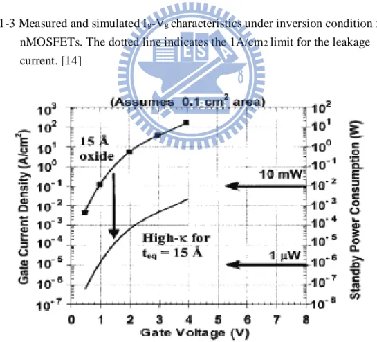
Fig. 1-3 Measured and simulated Ig-Vg characteristics under inversion condition for
nMOSFETs. The dotted line indicates the 1A/cm2 limit for the leakage
current. [14]
Figure-chapter 2
Fig. 2-1 ALCVD growth mechanism of AL2O3 and HfO2.
(International SEMATECH Confidential and Supplier Sensitive, 2002) Fig. 2-2 The ICP plasma system that was used in this experiment.
Fig. 2-3 The E-gun system that was used in this experiment. Fig. 2-4 The fabrication flow of the experiment.
x
Figure-chapter 3
Fig. 3-1 The capacitor C-V of HfSiOx characteristics for different RTA
temperatures and times with Al gate electrode.
Fig. 3-2 The capacitor C-V of HfSiOx characteristics for different RTA
temperatures and times with Al and Ti or Al gate electrode.
Fig. 3-3 The I-V characteristics of HfSiOx for different RTA temperatures and times
with Al gate electrode.
Fig. 3-4 The I-V characteristics of HfSiOx for different RTA temperatures and times
with Al and Ti or Al gate electrode.
Fig. 3-5 The C-V characteristics of HfSiOx for N2 plasma treatment compare with
different times.
Fig. 3-6 The C-V characteristics of HfSiOx for N2O plasma treatment compare with
different times.
Fig. 3-7 The C-V characteristics of HfSiOx for NH3 plasma treatment compare with
different times.
Fig. 3-8 The C-V characteristics of HfSiOx for CF4 plasma treatment compare with
different times.
Fig. 3-9 The I-V characteristics of HfSiOx for N2 plasma treatment compare with
different times.
Fig. 3-10 The I-V characteristics of HfSiOx for N2O plasma treatment compare with
different times.
Fig. 3-11 The I-V characteristics of HfSiOx for NH3 plasma treatment compare with
Fig 3-12 The I-V characteristics of HfSiOx for CF4 plasma treatment compare with
different times.
Fig. 3-13 The C-V characteristics of 3 nm HfSiOx gate dielectric Compared with
different plasma treatments.
Fig. 3-14 The C-V characteristics of 5 nm HfSiOx gate dielectric Compared with
different plasma treatments.
Fig. 3-15 The I-V characteristics of 3 nm HfSiOx gate dielectric Compared with
different plasma treatments.
Fig. 3-16 The I-V characteristics of 5 nm HfSiOx gate dielectric Compared with
different plasma treatments.
Fig. 3-17 The C-V characteristics of HfSiOx for N2 plasma treatment then CF4
plasma treatment.
Fig. 3-18 The C-V characteristics of HfSiOx for N2O plasma treatment then CF4
plasma treatment.
Fig. 3-19 The C-V characteristics of HfSiOx for NH3 plasma treatment then CF4
plasma treatment.
Fig. 3-20 The I-V characteristics of HfSiOx for N2 plasma treatment then CF4
plasma treatment.
Fig. 3-21 The I-V characteristics of HfSiOx for N2O plasma treatment then CF4
plasma treatment.
Fig. 3-22 The I-V characteristics of HfSiOx for NH3 plasma treatment then CF4
plasma treatment.
Figure-chapter 4
xii
treatment.
Fig. 4-2 The hysteresis of HfSiOx gate dielectrics with RTA 500oC 60 seconds.
Fig. 4-3 The hysteresis of HfSiOx gate dielectrics with RTA 500oC 60 seconds and
N2 plasma 60 seconds.
Fig. 4-4 The hysteresis of HfSiOx gate dielectrics with RTA 500oC 60 seconds and
N2O plasma 60 seconds.
Fig. 4-5 The hysteresis of HfSiOx gate dielectrics with RTA 500oC 60 seconds and
NH3 plasma 30 seconds.
Fig. 4-6 The hysteresis of HfSiOx gate dielectrics with RTA 500oC 60 seconds and
CF4 plasma 60 seconds.
Fig. 4-7 The hysteresis of HfSiOx gate dielectrics with RTA 500oC 60 seconds and
N2 plasma 60 seconds then CF4 plasma 60 seconds.
Fig. 4-8 The hysteresis of HfSiOx gate dielectrics with RTA 500oC 60 seconds and
N2O plasma 60 seconds then CF4 plasma 60 seconds.
Fig. 4-9 The hysteresis of HfSiOx gate dielectrics with RTA 500oC 60 seconds and
NH3 plasma 30 seconds then CF4 plasma 60 seconds.
Fig. 4-10 Gate current shift of HfSiOx gate dielectrics treated with N2 and CF4
plasma treatment during Vg = 5V CVS.
Fig. 4-11 Gate current shift of HfSiOx gate dielectrics treated with N2Oand CF4
plasma treatment during Vg = 5V CVS.
Fig. 4-12 Gate current shift of HfSiOx gate dielectrics treated with NH3 and CF4
Chapter 1
Introduction
1.1 Background
According to the recent prediction which was made by the Semiconductor Industry Association (SIA) in International Technology Roadmap for Semiconductors (ITRS) [1]-[3], the IC technology will continue its historical rate of advancement with Moore’s law for at least a couple of decades. ”Moore’s Law”, proposed by Gordon Moore in 1965, which states that “ The number of transistors and resistors on a chip doubles every 18 months ”, so it is needed to pursue better performance with lower cost. In order to achieve the goal, the scaling down of the device dimension is an inevitable tendency. The IC industry has been rapidly and consistently scaling down the design rule, increasing the chip and wafer size, and cleverly improving the design of devices and circuits for over 35 years [1]-[3].
In the scaling of CMOS, reducing the thickness of gate stack with lower leakage current plays an important role. Although the leakage current of the devices with the same gate dielectric reduces with the scaling gate length and width, that leakage current density increases with the scaling of gate dielectrics exponentially, the thickness of gate oxide have to be below 10 Å after 2007. Therefore, the gate leakage current increases as the device size decreases. The larger leakage current will not only cause the higher power consumption but also degrade the reliability of the devices. [4]-[5]
2
In terms of the first order current-voltage relation, the driving current of a
MOSFET can be given as
Where VGS is the applied gate to source, Leff is the effective channel length, W is the
channel width, Vt is the threshold voltage, μn is the mobility for electrons, Cg is the
gate capacitance, κ is the dielectric constant, ε0 is the permittivity of free space and tinv
is the electrical film thickness. From the formula, we know that with reduced threshold voltage, smaller effective channel length, and increased gate capacitance as well as gate-to-source voltage, the device can achieve better current driving ability. Of course, it can also have higher device density, which means a better performance and
much more transistors on the chip. However, a large VGS will degrade the reliability
while too small Vt will result in statistical fluctuation in thermal energy at a typical
operation circumstance of up to 100℃. So a bigger Cg and shorter Leff will be needed
to maintain device performance.
Using the material with high dielectric constant (high-k), the physical thickness of the dielectric in the devices can be increased without the reduction of capacitance density. Since the leakage current is related to the physical thickness, the increasing thickness of high-k dielectric can reduce the leakage current of the devices. Although high k dielectrics often exhibits smaller band gap, weaker bond, and higher defect
density than SiO2, the high k dielectrics with the same effective oxide thickness (EOT)
That is the reason why high-k dielectrics have drawn much attention for future gate dielectrics. Recently, some high-k dielectrics have been widely studied and the characteristics and issues of those materials have also been reported. The high-k dielectrics show good performances are always accompanied by another drawbacks. Finding out the most suitable high-k dielectric for the use of device and altering the device structure or process to meet the requirement of the high-speed device are significant tasks to implant high-k dielectrics to the next VLSI generation.
1.2 Scaling down of oxide thickness
According to the SIA (Semiconductor Industry Association) roadmap, CMOS with gate length below 70 nm will need an oxide thickness of less than 1.5 nm, which corresponds to two or three layers of silicon dioxide atoms. Reducing the thickness of silicon dioxide to these dimensions would result in an exponential increase of direct tunneling current [8]. The resulting gate leakage current will increase the power dissipation and decrease the device performance and circuit stability for VLSI circuits. The Fig.1-1 shows the possible conduction mechanism of the leakage current passing through the oxide , it could see there are several kinds of conduction mechanisms of the leakage current passing through the oxide layer, which contain hot carrier injection、Fowler-Nordheim tunneling and direct tunneling. When the oxide thickness is less than 2 nm, the dominant leakage mechanism is direct tunneling. This results that the leakage current increase rapidly with the decrease of the oxide thickness. We can see the machine from (1.3)
4
From Fig.1-2, when the equivalent oxide thickness (EOT) is 2 nm, the leakage current
density of SiO2 is 10-2 A/cm2, which is lower than logic limit but higher than wireless
limit. We could use SiON to replace SiO2 and reduce the leakage current density
about one order to make it lower than wireless limit. However, when the EOT is less than 2 nm, SiON also couldn’t be used for wireless application. In addition, the
leakage of SiO2 even is larger than logic limit when the EOT is down to 1.5 nm. SiON
also couldn’t be used for logic application when the EOT is less than 1.3 nm.
Therefore, we must use high-k materials instead of SiO2 to be the gate dielectric.
High-k dielectrics could effectively reduce the leakage current density about 4 orders.
We also can see the gate leakage current of scaling down of SiO2 from Fig.1-3.
Table 1-1 is the roadmap of 2006 (update) ITRS (International Technology Roadmap for Semiconductor) for the high performance logic technology. According to the projection of the International Technology Roadmap for Semiconductors, an equivalent oxide thickness of less than 1.0 nm is required for sub-65-nm metal–oxide–semiconductor field-effect transistor (MOSFET) devices [9]. Due to a
high tunneling leakage current, the scaling of SiO2 below 1.0 nm with an acceptable
leakage current level is very difficult. Recently, high-dielectric constant (high-k)
oxide thin films have attracted great interest as a replacement for nitrided SiO2 gate
oxide films [10]-[14].
(1.2) can be rewritten as follows:
From (1.4) we can see that if we increase the gate dielectric thickness and as usual retain the same Cg value, the leakage current problem could be solved.
1.3 High-k materials
1.3.1 The advantages of high-k dielectric
High-k gate materials can maintain the same EOT with thicker physical thickness, and is therefore expected drastically reduced direct-tunneling current. From Fig1-4, the increased physical thickness significant reduces the probability of tunneling across the insulator, and hence, reduces the amount of off-state leakage current density. [15]
The relationship between dielectrics constant and thickness is followed:
A suitable replacement gate dielectric with a high permittivity (k) must exhibit low leakage current, have the ability to be integrated into a CMOS process flow, and
exhibit at least the same equivalent capacitance, performance, and reliability of SiO2.
1.3.2 Challenges of high-k material
Although high-k material is expected to replace SiO2 ideally, there are many
problems to use high-k material practically. The issues for choosing a high-k material may include:
(1) Low dielectric constant interfacial layer between substrate and high-k material
(2) Degradation of carrier mobility (3) Shift of threshold voltage (4) Thermal stability
6
(5) Boron penetration prevention
(6) Poly interface and poly gate electrode
(7) Compatibility with traditional CMOS process.
1.3.3 The choice of high-k materials
It is important to discuss the general requirements and challenges associated with different High-k materials as possible gate dielectrics. Issues to be discussed include processing, dielectric constant, capacitance, bandgap, tunnel current, and reliability. In
the past three decades, SiO2 has served as an ideal gate dielectric, its several
advantages, such as being amorphous phase through the whole integration processing, high quality interface and good thermal stability, can indeed serve as a good guide of choosing high-k material. So, an ideal gate dielectric should meet the following requirements below:
Physical properties :
a. Suitable high k value (12~60)A suitable k value is indispensable. Those with not enough high k value could not satisfy (1.3) to lower the leakage by increasing physical thickness. While those with too high k value, in general, would suffer from thermal stability issues and larger fringing field.
b. Wide bandgap with conduction band offset > 1eV
It is found that most of the high-k materials do not have wide enough bandgap. In contact with silicon and gate electrode, the bandgap is closely related to the barrier height for carrier transport. Low bandgap will lead to intolerably high gate leakage (leakage current ~exp(-△ Ec)).
c. Thermodynamic stability in direct contact with silicon Preserve capacitance of gate stack after processing.
d. Film morphology (amorphous) and stable process compatibility
In the VLSI process, the thermal budget is an important issue since
high temperature changes dielectric phase. Once the gate dielectric material has transformed to polycrystalline from amorphous phase, the large grain boundaries would serve as leakage path, and induce large leakage current. e. Gate material compatibility
Materials such as metal gate, and metals have been considered for better controllability and better performance.
Electrical properties :
(a)Low interface state density (Dit< 5x10¹⁰/cm2-eV-1), and SiO2-like mobility, The
interface would affect the carrier mobility in the channel, and from (1.2), mobility degradation is related to poor current drivability. In high-k, there are so many sources that would reduce mobility, such as fixed charge, remote phonon, interfacial dipoles, remote surface roughness, surface roughness and phase separation crystallization. And most of them can be avoided by improving process technology.
(b) Tinv<1nm,
(c) J<10-3A/cm2@ VDD,
(d) VFB and hysteresis < 20mV,
(e) No C-V dispersion, (f) Reliability issue.
To serve as a new gate dielectric, we must also take into consideration electrical reliabilities, such as stress-induced leakage current (SILC), time dependent dielectric breakdown (TDDB), hot carrier aging, bias temperature instability and charge trapping issues [16].
8
1.3.4 Why choose HfSiO
x-base
There are many kinds of high-k materials, including Al2O3, Y2O3, Ta2O5, TiO2,
ZrO2 and HfO2 etc. Table 1-2 lists basic characteristics of several high-k dielectrics.
Unfortunately, many high-k materials such as Ta2O5, TiO2, SrTiO3 are thermally
unstable when directly contacted with silicon [17] and need an additional barrier layer which may add process complexity and impose thickness scaling limit. Also, materials with too low or too high dielectric constant may not be adequate choice for alternative gate dielectric application. Ultra high-k materials such as STO or BST may cause fringing field induced barrier lowering effect [18]. Materials with relatively low
dielectric constant such as A12O3 and Y2O3 do not provide sufficient advantages over
SiO2 or Si3N4 [19]. Among the medium-k materials compatible with silicon, oxides of
Zr and Hf are attracting much attention recently. Especially, Hf forms the most stable oxide with the highest heat of formation (ΔHf = 27l Kcal/mol) among the elements in IVA group of the periodic table (i.e. Ti, Zr, Hf). Unlike other silicides, the silicide of
Hf can be easily oxidized [20]. HfSiOx possesses a dielectric constant of up to 25 [21],
a large bandgap of 5.7 eV with sufficient band offset of larger than 1.5 eV [22], and
well thermal stability in contact with silicon [23]. HfSiOx is very resistive to impurity
diffusion and intermixing at the interface because of its high density (9.68 g/cm3) [24].
In addition, HfSiOx is the first high-k material showing compatibility with polysilicon
gate process [25]. These properties make HfSiOx to be one of the most promising
candidates for alternative gate dielectric application. Although inadequate mobility of
HfSiOx MOSFETs is among the biggest concerns, various techniques have been
explored to enhance the mobility. Introduction of strained silicon substrate [26], for example, drastically improved the mobility by changing the band structure of the substrate rather than changing the dielectric itself. However, the characteristics and
mechanism of HfSiOx are not totally understood.
1.4 Plasma nitridation
According to traditional view of improving SiO2 device performance, we could
find that nitridation is a common method to improve the interface. [27] Property with
the result that there is often Nit or Dit in the interface, imperfect bonding of interface
usually makes the characteristic of the device deteriorate. Such as charge will be trapped by the defects of the interface, it produce flat band voltage shift and also reduce mobility. Another shortcoming is that these dangling bonds will easily bond with oxygen atom in the following high temperature environment. The extra chemical reaction will let the interfacial oxide growth, and it will reduce the C value because of the lower dielectric constant. In addition, the quality of interfacial layer formed by oxidation is worse, and it would cause the problem of charge trapping. In order to solve these problems, nitridation treatment could let the atom of nitrogen bond with these dangling bonds and fix it while entering the interface layer, and then improve the stability and reliability of interface. Consequently, nitridation treatment is a workable solution to improve interface quality. As we note before, the question about
using high-k materials to replace SiO2 is that there are too many defects in the
interface to cause reliability degradation. Therefore, when we use high-k materials, it is consider that nitridation treatment is a more suitable way to improve reliability and thermal stability of device. These kind of treatment have already used in some relevant references. [28]-[29] Among them, someone take nitridation treatment at
high temperature, others take so-called plasma nitridation . According to [30], we
could understand that the effect of plasma nitridation is better than thermal nitridation. The reason is that high-k materials could not sustain high thermal stress. As long as
10
the temperature reaches certain degree, we would see the phenomenon of crystallization. The crystallization of dielectric would increase leakage current substantially, because it offers the path of leakage current. On the other hand, the meaning of plasma nitridation is to activate the source gas first. The high activation energy of radical will provide better mend which is better than nitridation at high temperature. For all these reasons, we adopt plasma nitridation in present experience.
1.5 Thesis organization
Following chapters in the thesis are primarily organized as follow:
In chapter 2, we make a description of experimental details. Atomic Layer Deposition system is used to deposit hafnium-based materials on silicon surface.
In chapter 3, we discuss the characteristics of HfO2 or HfAlOx insulator by
Metal-Insulator-Semiconductor (MIS) capacitors.
In chapter 4, we discuss the reliability of HfO2 or HfAlOx insulator by
Metal-Insulator-Semiconductor (MIS) capacitors and the effects of
Post-Metallization-Annealing.
In chapter 5, we make the conclusions for this thesis and provide some suggestions for future work.
Chapter 2
Experiments of Al-Ti-HfSiO
x-Si MIS capacitor
2.1 Use MOCVD to prepare high-k thin film
There are several ways to prepare high-k thin films, such as chemical vapor deposition (i.e. ALCVD, MOCVD, PECVD etc.) [30]-[32] and physical vapor deposition (i.e. Sputtering, E-gun, PLD etc.) [33]-[34]. ALCVD and MOCVD are the
usual ways for preparing HfSiOx films; and E-gun is the convenience way for
preparing HfSiOx films. We used the MOCVD methods below.
MOCVD (metal-organic CVD) is a widely used technology for depositing a variety of thin films, including metal oxide and metal silicate films, for high-k gate dielectric applications. The basic steps in MOCVD deposition method are as follows:
1. MO precursor in company with N2 process gas and O2 process gas are injected
into the reactor.
2. The sources are mixed inside the reactor and transferred to the deposition process chamber.
3. At the deposition process chamber, high temperature results in the decomposition of sources and other gas-phase reactions, forming the film precursors that are useful for film growth and byproducts.
4. The film precursors transport to the growth surface. 5. The film precursors absorb on the growth surface. 6. The film precursors diffuse to the growth site.
12
7. At the surface, film atoms incorporate into the growing film through surface reaction.
8. The byproducts of the surface reactions desorb from the surface.
9. The byproducts transport to the main gas flow region away from the deposition area toward the reaction. Then the wafer exits.
From fig. 2-1, it is apparent that 1 nm EOT can be achieved with MOCVD metal oxide films when a metal electrode is used. However, most of the devices with
MOCVD HfSiOx when a poly-Si gate is used have EOT greater than 2 nm. Unlike
metal electrode, using poly-Si electrode requires the high-k gate stack to go through a 1000°C/10 second S/D activation anneal step. This step not only results in chemical and structural changes in the high-K film, but also affects interfaces between the high-k film/substrate and the high-k/poly-Si electrode. All devices fabricated with
MOCVD ZrO2 and ZrSiO films using poly-Si gate electrode were too leaky to give
any meaningful C-V results. In general, using poly-Si gate electrode results in around
0.7 to 1 nm higher EOT for gate stacks fabricated with HfSiOx gate dielectric films.
This additional interfacial oxide thickness is too large to be acceptable. In view of this, the MOCVD is not a good tool for high-k material deposition with poly-Si gate. However, the MOCVD has very good throughput and can process a 25-wafer lot in ~2 hours (roughly 4X better than ALCVD). Thus, from a throughput perspective, the MOCVD has a distinct advantage over the ALCVD [35].
2.2 Rapid thermal annealing system
Metal RTA-AG 610 was a single-wafer lamp-heated and computer-controlled rapid thermal processing (RTP) system. Water and compressed dry air (CDA) cooling system were used to cool down the quartz chamber. High intensity visible radiation
heating and cold-heating chamber walls allow fast wafer heating and cooling rate. The tungsten halogen lamps were distinguished into five groups, and the relative percentage of lamp intensity can be adjusted individually for each group to achieve uniform temperature distribution. Temperature was obtained from pyrometer and precise controlled by computer. Two gas lines were used in the system which can be
switched between Ar and N2. Before RTA process started, one minute N2 gas purge
was performed to minimize the water vapor introduced during wafer loading and also swept unwanted particles induced during process. A fast heating rate of 100℃/s was chosen in this work. When anneal was complete, chamber temperature was quickly
cooled down from 900℃ to 500℃ by N2 purge 30 seconds. Then, the chamber was
slowly cooled down to 280℃ without N2 purge to avoid creaking of films. After five minutes later, wafers can be taken out from the chamber. Films’ creak can be avoided by two-steps-cooling method.
2.3 Plasma treatment system
When the PDA (Post-Deposition-Annealing) was finished, some samples were subjected to an additional plasma treatment in order to improve the electrical
properties of gate dielectric. There were various source gas (N2, N2O, NH3, CF3) and
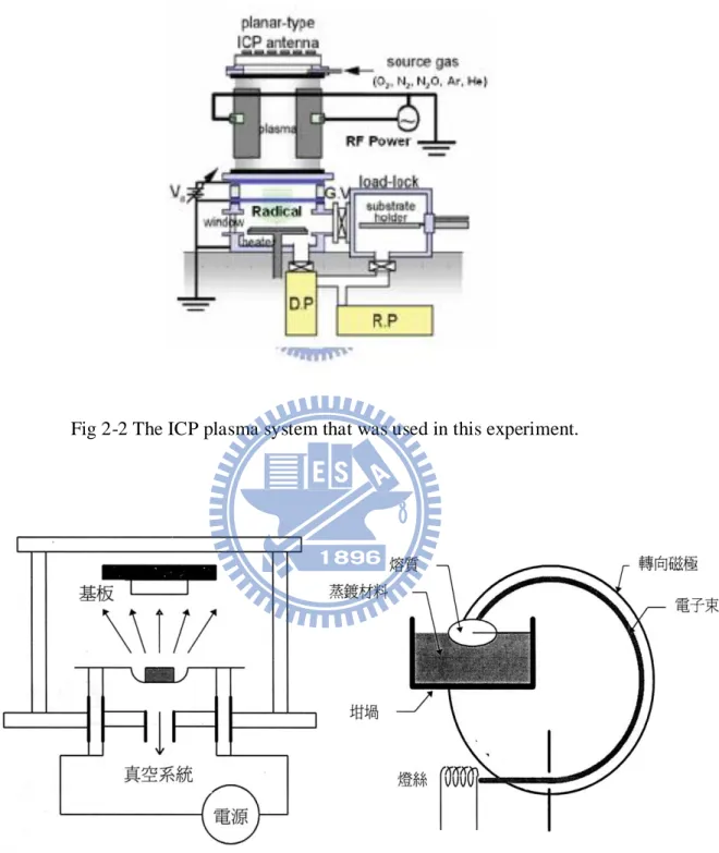
process time (30~120 seconds) as the experiment conditions. Parallel plate high-density plasma reactor employing an ICP source was a single-wafer treated and computer-controlled system.
Fig. 2.2 illustrates ICP system that was used in this experiment. 13.56 MHz RF power was coupled to the top electrode through a matching network. After the sample load to reactor, the system was pumped down to keep the chamber clean enough. Subsequently, the source gas was become radical by the plasma system, as the
14
chamber pressure was 100 mTorr and the substrate temperature was 300℃ so that to achieve the goal of low temperature process. The power of working plasma was kept constant at 200W and the flow rate of source gas was 100 sccm. While the process of plasma treatment was finished, these samples were brought to thermal treatment to reduce plasma damage.
2.4 E-gun
After plasma treatment and PNA, we deposited Ti and Al as electrical by E-gun. And finished all manufacturing process, we used E-gun deposited Al as back electrical too.
Figure 2-3 shows E-gun work theorem, the system is always in vacuity, and the materials which we wanted to deposited was in the boat. We melt down the materials by heating, and using the electron-beam to bombard the materials to proceed
evaporation. The chamber pressure was 10-6 mTorr when we deposited. After the
deposited Ti and Al we could proceed lithography and etching.
2.5 MIS capacitors fabrication process
In this thesis, Al-Ti-HfSiOx-Si MIS capacitors were fabricated to study ultra thin
HfSiOx gate dielectrics. Figure 2-4 shows the fabrication flow of this experiment. The
starting wafer was four inch (100) orientated p-type wafer. It was one side polished and its resistivity was 5~10 ohm-cm.
After standard initial RCA cleaning, wafers were put into chamber and grew
HfSiOx layer with atomic layer deposition system. After the thin films were prepared,
subjected to an additional plasma treatment at the substrate temperature of 300℃ while the pressure was 100 mTorr and the plasma power was 200W. The plasma
treatment conditions were in pure N2, N2O, NH3, and CF3 for 30~120 seconds
respectively and the flow rate were 100 sccm. After nitridation, we also annealed these samples to reduce the plasma damage. Finally, pure Ti and Al films were thermally evaporated on the top side of wafers. Mask defined the top electrode. Then,
we used wet etching to etch undefined Al, Ti and HfSiOx films. After patterning,
backside native oxide was stripped with diluted HF solution, and Al was deposited as bottom electrode. The detailed fabrication process flow was listed as follows.
1. Initial RCA cleaning.
2. Atomic layer deposition HfSiOx .
3. Post-deposition anneal with 500℃ 60 seconds for HfSiOx .
4. Plasma treatment with N2,N2O, NH3 and CF3 plasma for 30~90 seconds
respectively.
5. Post-nitridation annealing with 600℃ 30seconds.
6. Thermally evaporate 200 Å titanium 4000 Å aluminum as the top electrode.
7. Mask: define top electrode and then wet etch undefined Al, Ti and HfSiOx films.
16
After the Al/ Ti/ HfO2 /Si MIS capacitors were prepared, we used semiconductor
parameter analyzer (HP4156A) and C-V measurement (HP4284) to analysis electric characteristics (i.e. I-V, C-V, EOT, leakage current density etc.). Then we tested their reliability, including constant voltage stress (CVS), Hysteresis effect.
Chapter 3
Electrical characteristics of Al-Ti- HfSiO
x-Si MIS
capacitors
3.1 Electrical characteristics of capacitors with different
post-deposition annealing temperature
3.1.1 Capacitance-voltage characteristics for HfSiO
xwith
different gate electrodes
In order to measure the C-V characteristics of our MIS capacitors, we used HP 4284A precision LCR meter in our experiments. We swept the gate bias from accumulation region to inversion region to obtain the curve at the frequency of 50 kHz from -2V to 1V. Then, the effects of different post deposition annealing (PDA)
temperature (i.e. 500oC, 600oC, 800oC) and different post deposition annealing times
(i.e. 30seconds, 60seconds, 90seconds, 120seconds) and different plasma treatment
source (i.e. N2, N2O, NH3, CF4) will be discussed.
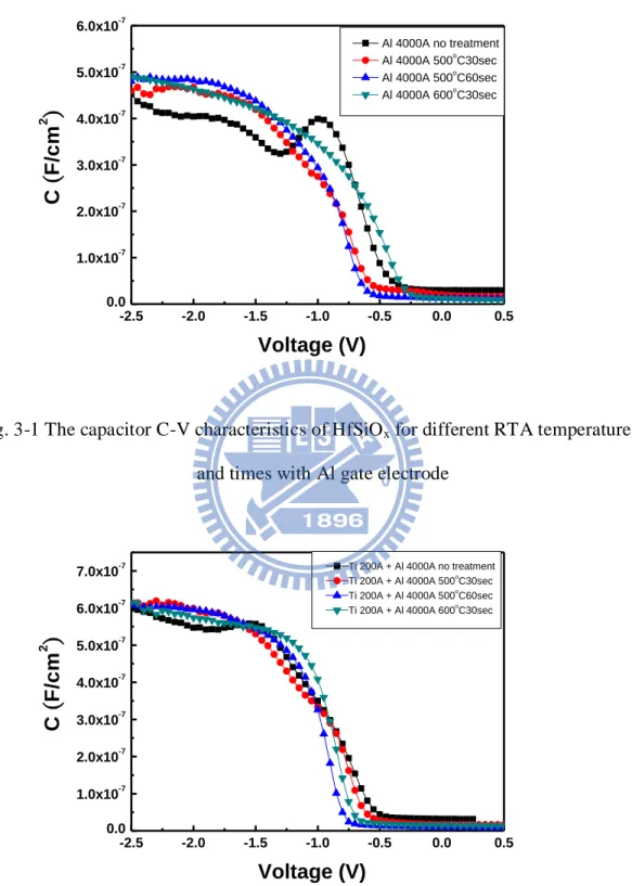
Fig. 3-1 shows the capacitance-voltage (C-V) characteristic of HfSiOx gate
dielectrics and Al gate electrode treated with different annealing temperatures for different process time. PDA could reduce the flat-band voltage and make the thin film
18
Fig. 3-2 shows the C-V characteristic of HfSiOx gate dielectrics and A+Til gate
electrode treated with different annealing temperatures for different process time. In this case, the capacitances treated with PDA 500oC 60 seconds had the best capacitance too.
3.1.2 Leakage current-voltage characteristics for HfSiO
xwith different gate electrodes
The leakage current of our MIS capacitors were analyzed from the current -voltage (I-V) characteristics measured by an HP4156A semiconductor parameter analyzer.
Fig. 3-3 shows the I-V characteristics of HfSiOx gate dielectrics and Al gate
electrode treated with different annealing temperatures for different process time from 0V to -2V. The gate leakage current density of these samples after PDA could be decreased, because the film became dense after PDA. And the lowest condition is
PDA at 500oC 30 seconds.
Fig. 3-4 shows the I-V characteristics of HfSiOx gate dielectrics and Al+Ti gate
electrode treated with different annealing temperatures for different process time from 0V to -2V. The gate leakage current density of these samples after PDA could be decreased, because the film became dense after PDA. And the lowest condition is
PDA at 500oC 30 seconds.
We compared two gate electrodes, Ti-Al gate had larger capacitance and lower
3.2 Electrical characteristics capacitors with different
plasma treatment for different process time
There are three kinds of plasma treatment with different source gas (i.e. N2, N2O,
NH3 and CF4) and they were treated for different process time (i.e. 30 seconds, 60
seconds, 90 seconds and 120 seconds). And, the relationship of difference process time in one kind of plasma treatment will be discussed.
3.2.1 Capacitance-voltage characteristics for HfSiO
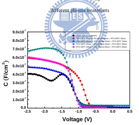
xFig 3-5 shows the capacitance-voltage (C-V) characteristics of HfSiOx gate
dielectrics after PDA at 500oC 60 seconds and treated with N2 plasma treatment of
200W for different process time. The capacitor treated for 60 seconds shows the maximum capacitance among three conditions of process time. Furthermore, the
capacitor treated with N2 plasma both show the good capacitance values which are
larger than the capacitor which was not treated by N2 plasma.
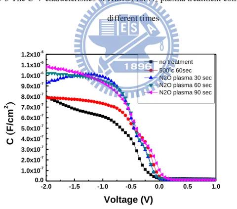
Fig. 3-6 shows the capacitance-voltage (C-V) characteristics of HfSiOx gate
dielectrics after PDA at 500oC 60 seconds and treated with N2O plasma treatment of
200W for different process time. At this condition, the capacitor treated for 90 seconds shows the maximum capacitance among four conditions of process time. But
for the capacitance treated with N2O plasma for 60 seconds shows the best C-V curve.
Fig. 3-7 shows the capacitance-voltage (C-V) characteristics of HfSiOx gate
dielectrics after PDA at 500oC 60 seconds and treated with NH3 plasma treatment of
200W for different process time. Just like the samples of N2 plasma treatment. The
improvement of capacitance could be seen. At this condition, the capacitance treated
with NH3 plasma for 30 seconds shows the largest value. By the way, all the samples
20
is indicated that NH3 plasma treatment is also a practicable method to improve the
capacitance -voltage characteristics of HfSiO2 gate dielectrics.
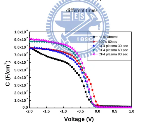
Fig 3-8 shows the capacitance-voltage (C-V) characteristics of HfSiOx gate
dielectrics after PDA at 500oC 60 seconds and treated with CF4 plasma treatment of
200W for different process time. The capacitor treated for 60 seconds and 90 seconds all shows the maximum capacitance among three conditions of process time. Furthermore, the capacitors after post plasma annealing treated show the larger capacitance values and show the better than the capacitors which have no annealing treatment after plasma.
When the N2 plasma process time over 90 sec, the C value will become smaller,
we think that it is may be caused by the growing of interfacial oxide in the plasma
process time. The same phenomenon is also found on N2O, NH3 and CF4 plasma.
3.2.2 Leakage current-voltage characteristics for HfSiO
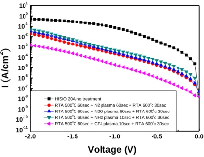
xFig. 3-9 shows the I-V characteristics of p-type HfSiOx capacitors after PDA at
500oC 60 seconds and treated by N2 plasma of 200W with different process time from
0V to -2V. We observed that the gate leakage current density is suppressed while N2
plasam treatment. It is indicated that N2 plasma treatment supply an effective barrier
against the leakage current. The film after N2 plasma treatment became dense and
strong, so the leakage current could be effectively decreased, especially for capacitor
which treated with N2 plasma 30 seconds has the lowest leakage. Gate leakage current
density of no treatment insulator at Vg = -1V is about 7 10-2 A/cm2. However, gate
leakage current density of the capacitor treated for 30 sec N2 plasma at Vg = -1V is
about 5 10-5 A/cm2. It has less gate leakage than no treatment insulator about 2~3
Fig. 3-10 shows the I-V characteristics of p-type HfSiOx capacitors after PDA at
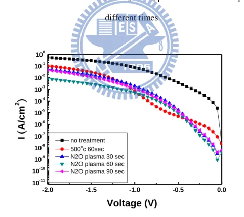
500oC 60 seconds and treated by N2O plasma of 200W with different process time
from 0V to -2V. After N2O plasma treatment, we could see the reduction of leakage
current in contrast of no treatment samples. However, the sample of plasma treated for 60 seconds got the smallest gate leakage current and a good C-V curve from Fig 3-6.
Fig. 3-11 shows the I-V characteristics of p-type HfSiOx capacitors after PDA at
500oC 60 seconds and treated by NH3 plasma of 200W with different process time
from 0V to -2V. After NH3 plasma treatment, we could see the reduction of leakage
current in contrast of no treatment samples. However, the sample of plasma treated for 90 seconds got the smallest gate leakage current. Compare with the sample which no treated by plasma, the leakage current would lower about 3 order.
Fig. 3-12 shows the I-V characteristics of p-type HfSiOx capacitors after PDA at
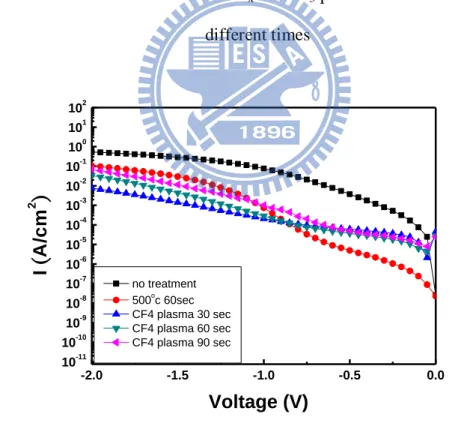
500oC 60 seconds and treated by CF4 plasma of 200W with different process time
from 0 V to -2V. After CF4 plasma treatment, we can see much reduction of leakage
current in contrast of no treatment samples. It is worthy to be noticed that all the
capacitors treated by CF4 plasma have a low leakage current about 2×10⁻⁴ A/cm2 at
Vg = -1V. We can clearly see the F element will effectively repair defect, can let leakage current seriously decrease.
As a consequence, the N2, N2O, NH3 CF4 plasma treatment all shows better
electrical properties than no treatment sample. Furthermore, the N element, O element and F element all could fix the interface and improve the electrical properties include of C-V curve and I-V curve.
22
3.3 Electrical characteristics of capacitors with different gate
dielectric thickness
We have four kinds of plasma treatment with different source gas (i.e. N2, N2O,
NH3) and treated for different process time (i.e. 30 seconds, 60 seconds and 90
seconds). Then we compare the effect of different source gas with different thickness.
3.3.1 Capacitance-voltage characteristics for HfSiO
xFig. 3-13 shows C-V characteristics of 3nm HfSiOx gate dielectrics after PDA at
500oC 60 seconds and treated with N2 plasma treatment for 60 seconds, N2O plasma
treatment for 60 seconds and NH3 plasma treatment for 30 seconds. It is indicated that
the capacitances treated with N2 plasma for 60 seconds and NH3 plasma for 30
seconds show the most excellent value (i.e. 30% increasing about capacitance).
Among these samples, the reason why the sample treated with N2O plasma has lower
capacitance than N2 and NH3 plasma treatment is complex. It is may be the growing
of interfacial oxide made the C value smaller and this interfacial layer also made the gate leakage current smaller. But for the reason of oxidation caused by oxygen radical,
the N2O plasma treatment samples show the lower C value.
Fig. 3-14 shows C-V characteristics of 5nm HfSiOx gate dielectrics after PDA at
500oC 60 seconds and treated with N2 plasma treatment for 60 seconds, N2O plasma
treatment for 60 seconds and NH3 plasma treatment for 30 seconds. It is indicated that
the capacitance treated with NH3 plasma for 30 seconds shows the most excellent
value (i.e. 60% increasing about capacitance).
Fig. 3-15 and Fig. 3-16 show I-V characteristics of 3nm and 5nm HfSiOx gate
dielectrics after PDA at 500oC 60 seconds and treated with N2 plasma treatment for 60
seconds, N2O plasma treatment for 60 seconds and NH3 plasma treatment for 30
seconds. It is indicated that the capacitances treated with plasma show the lower
leakage current. Especially for capacitor which treated with N2 plasma 30 seconds has
the lowest leakage.
3.4 Electrical characteristics of capacitors combined with
two plasma treatment for different process Time
Final, we try to combined two plasma treatment for different process time to see the electrical characteristics of P-type capacitors.
3.4.1 Capacitance-voltage characteristics for HfSiO
xFig. 3-17 shows C-V characteristics of HfSiOx gate dielectrics after PDA at
500oC 60 seconds and treated with N2 plasma treatment of 200W for 60 seconds, then
treated with CF4 plasma treatment for 30 or 120 seconds. It is indicated that the
capacitance treated with CF4 plasma for 30~60 seconds will increase effectively. And
the C-V curve became better. But the capacitance treated with CF4 plasma for 90~120
seconds will decrease, the result is maybe too long plasma treatment would cause plasma damage. It let the capacitance become lower. However, the N element and F element have a good collocation.
Fig. 3-18 shows C-V characteristics of HfSiOx gate dielectrics after PDA at
500oC 60 seconds and treated with N2O plasma treatment of 200W for 60 seconds,
24
capacitance treated with CF4 plasma for 60 seconds will increase effectively. And the
C-V curve became better. But same to N2 plasma, the capacitance treated with CF4
plasma for 120 seconds will decrease, the result is maybe too long plasma treatment would cause plasma damage. It let the capacitance become lower. However, the N and O element and F element have a good collocation.
Fig. 3-19 shows C-V characteristics of HfSiOx gate dielectrics after PDA at
500oC 60 seconds and treated with NH3 plasma treatment of 200W for 30 seconds,
then treated with CF4 plasma treatment for 30 or 120 seconds. It is indicated that the
capacitance treated with CF4 plasma for 60 seconds will increase effectively. And the
C-V curve became better than others. However, the N element and F element have a good collocation.
3.4.2 Leakage current-voltage characteristics for HfSiO
xFig. 3-20 shows I-V characteristics of HfSiOx gate dielectrics after PDA at
500oC 60 seconds and treated with N2 plasma treatment of 200W for 60 seconds, then
treated with CF4 plasma treatment for 30 or 120 seconds. It is indicated that after N2
plasma treatment only, the leakage current shows the lowest leakage current. But had
CF4 plasma will increase, this is maybe that the F element would etch HfSiOx, causing
the oxide became thinner and let the leakage current increase. The sample treated wit h
CF4 plasma 120 seconds was the most obvious.
Fig. 3-21 shows I-V characteristics of HfSiOx gate dielectrics after PDA at
500oC 60 seconds and treated with N2O plasma treatment of 200W for 60 seconds,
then treated with CF4 plasma treatment for 30 or 120 seconds. It is indicated that after
N2O plasma treatment only, the leakage current shows the lowest leakage current. But
causing the oxide became thinner and let the leakage current increase. The sample
treated with CF4 plasma 90~120 seconds was the most obvious.
Fig. 3-22 shows I-V characteristics of HfSiOx gate dielectrics after PDA at
500oC 60 seconds and treated with NH3 plasma treatment of 200W for 60 seconds,
then treated with CF4 plasma treatment for 30 or 120 seconds. It is indicated that after
NH3 plasma treatment only and with short time CF4 plasma like 30 seconds, the
leakage current shows the lowest leakage current. But had long time CF4 plasma will
increase, this is maybe that the F element would etch HfSiOx, causing the oxide
became thinner and let the leakage current increase. The sample treated with CF4
plasma 90~120 seconds was the most obvious.
After plasma treatment we always did post deposition annealing and post plasma treatment annealing, the sample without nitridation can not sustain the high temperature annealing, so nitridation can improve the thermal stability of high-k film. The sample without PDA and treated by plasma treatment directly is distorted at high negative bias voltages owing to the crystallization. It might be cause by plasma damage, therefore we must add the post-nitridation anneal step to restore the plasma damage. We could see that after post deposition anneal, nitridation could effectively improve the thermal stability of the thin film. We can find the same result, the sample with nitridation after PDA can effectively decrease gate leakage current. It is good evidence to show that the thin film treated by plasma treatment after post-deposition anneal can make the thin film sustain high thermal stress.
26
Chapter 4
Reliability of Al-Ti-HfSiO
x-Si MIS capacitors
4.1 Hysteresis
When a ferromagnetic material is magnetized in one direction, it will not relax back to zero magnetization when the applied magnetizing field is removed. It must be driven back to zero by the additional opposite direction magnetic field. If an alternating magnetic field is applied to the material, its magnetization will trace out a loop called a hysteresis loop. The lack of retrace ability of the magnetization curve is the property called hysteresis and it is related to the existence of magnetic domains in the material. Once the magnetic domains are reoriented, it takes some energy to turn them back again [36]. The hysteresis phenomenon is similar in the C-V curve of the MIS capacitor device. When we apply a voltage in opposite direction, it will not fit the original C-V curve measured previously. It is due to the traps of interface which would trap charges to influence the flat band voltage and C-V curve. [37]
Fig. 4-1 shows the hysteresis of p-type HfSiOx gate dielectric which was without
PDA. Fig. 4-2 shows the hysteresis of p-type HfO2 gate dielectric which was with
PDA 500oC 60 seconds but without plasma treatment. We see that, the hysteresis of
the thin film treated with annealing was much smaller than the thin film without annealing. It is a good way to do annealing ater deposited Hf-base dielectric, because its interfacial trap density could be removed after annealing. The hysteresis for capacitance which was with PDA is 44 mV.
Fig. 4-3 shows the hysteresis of p-type HfSiOx gate dielectrics with PDA 500oC
60 seconds、N2 plasma 60 seconds、and PNA 600oC 30 seconds. The hysteresis is 32
mV. Fig. 4-4 shows the hysteresis of p-type HfSiOx gate dielectrics with PDA 500oC
60 seconds、N2O plasma 60 seconds、and PNA 600oC 30 seconds. The hysteresis is 23
mV. Fig. 4-5 shows the hysteresis of p-type HfSiOx gate dielectrics with PDA 500oC
60 seconds、NH3 plasma 30 seconds、and PNA 600oC 30 seconds. The hysteresis is 26
mV. So nitridation could decrease the trap density and let the thin film sustain high thermal stress.
Fig. 4-6 shows the hysteresis of p-type HfSiOx gate dielectrics with PDA 500oC
60 seconds、CF4 plasma 60 seconds、and PNA 600oC 30 seconds. The hysteresis is 2
mV. Fig. 4-7 shows the hysteresis of p-type HfSiOx gate dielectrics with PDA 500oC
60 seconds、N2 plasma 60 seconds、CF4 plasma 60 seconds、and PNA 600oC 30
seconds. The hysteresis is 9 mV. Fig. 4-8 shows the hysteresis of p-type HfSiOx gate
dielectrics with PDA 500oC 60 seconds、N2O plasma 60 seconds、CF4 plasma 60
seconds、and PNA 600oC 30 seconds. The hysteresis is 16 mV. Fig. 4-9 shows the
hysteresis of p-type HfSiOx gate dielectrics with PDA 500oC 60 seconds、NH3 plasma
30 seconds、CF4 plasma 60 seconds、and PNA 600oC 30 seconds. The hysteresis is 12
mV. So fluorination could decrease the trap density and let the thin film sustain high thermal stress too and more clearly. As a consequence, the plasma treatment can improve the reliability of gate oxide.
4.2 Constant voltage stress (CVS)
To study the reliability of thin films, we can stress the samples with a constant voltage or a constant current, which are useful methods. The mechanism of CVS is the charge trapped by the interfacial trap density which is caused by stress for a long
28
time. In addition, the increasing interface trap density would cause new leakage path to add leakage current. In our experiments, we use constant voltage stress (CVS) to test the reliability of the thin film.
Fig. 4-10 shows gate current shift of p-type HfSiOx gate dielectrics treated with
N2 plasma treatment and CF4 plasma treatment during CVS with Vg = 5 V. It
indicated that the thin film with plasma treatment which current shift was smaller than
the original one. The sample with N2 plasma and CF4 plasma treatment also had much
smaller current shift but had large leakage current. Fig. 4-11 shows gate current shift
of p-type HfSiOx gate dielectrics treated with N2 plasma treatment and CF4 plasma
treatment during CVS with Vg = 5 V. It indicated that the thin film with plasma
treatment which current shift was smaller than the original one. The sample with N2O
plasma and CF4 plasma treatment also had much smaller current shift but had large
leakage current. Fig. 4-12 shows gate current shift of p-type HfSiOx gate dielectrics
treated with NH3 plasma treatment and CF4 plasma treatment during CVS with Vg =
5 V. It indicated that the thin film with plasma treatment which current shift was
smaller than the original one. The sample with N2 plasma and CF4 plasma treatment
also had much smaller current shift but had large leakage current.
The gate leakage shift level of the samples with or not nitridation differed about 3 to 4 orders, so nitridation process could decrease the trap density effectively. It might be a good way to incorporate N atoms in the thin film to improve the reliability of the gate dielectrics.
Chapter 5
Conclusions and future work
5.1 Conclusions
In this thesis, characteristics and reliability of HfSiOx gate dielectrics with the
post-deposition annealing (PDA) and the post plasma treatment (PNA) have been
investigated. These methods could be improved that the quality of HfSiOx thin film.
The plasma treatment conditions are N2, N2O, NH3 and CH4 plasma for 30 sec, 60 sec,
90 sec and 120 sec individually. After the post-deposition annealing (PDA), the plasma treatment and the post plasma treatment (PNA), our experimental data revealed low leakage current density and good thermal stability. We find several important phenomena and they would be summarized as follows.
First, improvement in the electrical characteristics of Al-Ti-HfSiOx-Si MIS
capacitors after post-deposition-annealing has been demonstrated in this work. The
HfSiOx thin film after PDA would become dense and we could find their capacitance
would increase and gate leakage current would decrease.
Second, all of the samples after plasma treatment can promote the electrical characteristics and reliability until the plasma damage happened. Among these
treatments, the sample treated by N2 plasma treatment for 60 sec, N2O plasma
treatment for 60 sec, NH3 plasma treatment for 30 sec and CF4 plasma treatment for
60 sec for HfSiOx represented a fairly great improvement, such as good capacitance
30
reduction for all samples ). It was showed that the interfacial layer could be
suppressed and the weak structure of interface has been repaired by N2 and NH3
plasma respectively. However, N2O plasma treatment also can provide good effects
on electrical characteristics. The samples treated N2O plasma treatment would
introduce oxygen bonding to form additional interfacial layer, so the capacitance
would be decreased a little. The sample treated by CF4 plasma also showed excellence
promotion about reliability issues, such as smaller hysteresis ( < 15 mV ) and better CVS curve.
Finally, in this thesis, it has been indicated that combined two kinds of plasma,
such as N2, NH3 and N2O plasma and then did the CF4 plasma treatment could
improve stress stability of HfSiOx thin film. Simultaneously, and the reliability of the
film after nitridation and fluorination also represented better electronic characteristics. The most suitable way for post-deposition treatment by plasma to improve electrical characteristics on MIS structure has been observed.
5.2 Future work
In this experiment, the HfSiOx film was deposited by MOCVD system. In the
future, the ALCVD ( Atomic Layer CVD ) system will become another important deposition technology. Further experiment and analysis are required to clarify if the same treatment condition is also suitable for ALCVD film. On the other hand, the MOSFET will be fabricated by the same treatment condition to verify the effect on device characteristics, such as mobility, subthreshold swing, and transonductance.
The interfacial layer between high-k/Si would be increased by increasing post-deposition-annealing temperature. In order to suppress the growth of the interfacial layer, we could use some pre-treatment methods to introduce a thin oxide
or nitride layer by HDP-PECVD or chemical deposition. Furthermore, we might have to understand the mechanism of leakage current of thin film and thick film individually. Finally, the mechanism of the generation of the defects in the high-k bulk or interface still needs to be solved.
32
References
[1] G.E. Moore, “Lithography and the future of Moore’s Law,” in Proc. Eighth Optical/Microlithography Conf., SPIE, vol. 2440, pp. 2–17, Feb. 1995.
[2] Semiconductor Industry Association (SIA), International Technology Roadmap for Semiconductors 2003 ed., Austin, TX: SEMATECH, 2003.
[3] P.M. Zeitzoff and J.E. Chung, “Weighing in on logic scaling trends,” IEEE Circuits Devices Mag., vol. 18, pp. 18–27, Mar. 2002.
[4] Wang Bin, J. S. Suehle, E. M. Vogel and J. B. Bernstein, ”Time-dependent breakdown of ultra-thin SiO2 gate dielectrics under pulsed biased stress,” IEEE Electron Device Lett., 22, pp. 224-226, 2001.
[5] J. H. Stathis, A. Vayshenker, P. R. Varekamp, E. Y. Wu, C. Montrose, J. McKenna, D. J. DiMaria, L. -K. Han, E. Cartier, R. A. Wachnik and B. P. Linder, “Breakdown measurements of ultra-thin SiO2 at low voltage,” in IEDM Tech. Dig, pp. 94-95, 2000.
[6] M. Koyama, K. Suguro, M. Yoshiki, Y. Kamimuta, M. Koike, M. Ohse, C. Hongo and A. Nishiyama, “Thermally stable ultra-thin nitrogen incorporated ZrO2 gate dielectric prepared by low temperature oxidation of ZrN,” in IEDM Tech. Dig, pp. 20.3.1-20.3.4, 2001
[7] E. P. Gusev, D. A. Buchanan, E. Cartier, A. Kumar, D. DiMaria, S. Guha, A. Callegari, S. Zafar, P. C. Jamison, D. A. Neumayer, M. Copel, M. A.
Bojarczuk, L. -A. Ragnarsson and Rons, “Ultrathin high-K gate stacks for advanced CMOS devices,” in IEDM Tech. Dig, pp. 20.1.1-20.1.4, 2001.
[8] Suehle, J. S.; Vogel, E. M.; Edelstein, M. D.; Richter, C. A.; Nguyen, N. V.; Levin,I.; Kaiser, D. L.; Wu, H.; Bernstein, J. B., “Challenges of high-k gate dielectrics for future MOS devices”, Plasma- and Process-Induced Damage,
2001 6th International Symposium on , 2001.
[9] “International Technology Roadmap for Semiconductors” 2005 Update, published by the Semiconductors Industry Association.
[10] C. S. Lai, W. C. Wu, J. C. Wang and T. S. Chao: Appl. Phys. Lett. 86 (2005) 22905.
[11] J. C. Wang, S. H. Chiao, C. L. Lee, T. F. Lei, Y. M. Lin, M. F. Wang, S. C. Chen, C. H. Yu and M. S. Liang: J. Appl. Phys. 92 (2002) 3936.
[13] L. F. Schn, R. B. van Dover and R. M. Fleming: Appl. Phys. Lett. 75 (1999) 1967.
[14] B. K. Park, J. Park, M. Cho, C. S. Hwang, K. Oh, Y. Han and D. Y. Yang: Appl. Phys. Lett. 80 (2002) 2368.
[15] G. D. Wilk, R. M. Wallace, et. al., “High-k gate dielectrics: current status and materials properties consideration” J. Appl. Phys., Vol. 89, No. 10, pp. 5243,2001.
34
[17] K. J. Hubbard and D. G. Schlom, J. Mater. Res. 11, 2757 (1996).
[18] Baohong Cheng, Min Cao, Ramgopal Rao, Anand Inani, Paul Vande
Voorde,Wayne M. Greene, Johannes M. C. Stork, Zhiping Yu, Peter M. Zeitzoff, Jason C.S. Woo, “The Impact of High-k Gate Dielectrics and Metal Gate
Electrodes on Sub-100 nm MOSFET’s”, IEEE Transactions on Electron Devices, Vol. 46, No. 7, July 1999.
[19] C. T. Liu, “Circuit Requirement and Integration Challenges of Thin Gate Dielectrics for Ultra Small MOSFET’s” in IEDM Tech. Dig., p.747, 1998.
[20] S. P. Muraka and C. C. Chang, Appl. Phys. Lett. 37,639 (1980).
[21] M. Balog, M. Schieber,M. Michman, and S. Patai, “Chemical vapor deposition and characterization of HfO2 films from organo-hafnium compounds,” Thin Solid Films, vol. 41, pp. 247–259, 1977.
[22] J. Robertson, “Band offsets of wide-band-gap oxides and implications for future electronic devices,” J. Vac. Sci. Technol. B, vol. 18, pp. 1785–1791, 2000.
[23] K. J. Hubbard and D. G. Schlom, “Thermodynamic stability of binary oxides in contact with silicon,” J. Mat. Res., vol. 11, pp. 2757–2776, 1996.
[24] M. Balog et al. Thin Solid Films, ~01.41, 247 (1977).
[25] K. Onishi, C. S. Kang, R. Choi, H.-J. Cho, S. Gopalan, R. Nieh, S. Krishnan, and J. C. Lee, “Effects of high-temperature forming gas anneal on HfO2 MOSFET performance,” in VLSI Tech. Dig, pp. 22–23, 2002.