A Millimeter-Wave Wideband SPDT Switch
with Traveling-Wave Concept Using 0.13-
µm CMOS Process
Mei-Chao Yeh, Zuo-Min Tsai, Kun-You Lin, Huei Wang, Chia-Yi Su*, and Chih-Ping Chao*
Dept. of Electrical Engineering and Graduate Institute of Communication Engineering,
National Taiwan University, Taipei, 106, Taiwan, R.O.C.
*Taiwan Semiconductor Manufacturing Company, Hsinchu City, 300, Taiwan, R.O.C.
Abstract — A wideband SPDT switch in standard bulk
0.13-µm CMOS process is demonstrated in this paper. In order to extend the operation frequency, the traveling-wave circuit topology is utilized. Due to the different requirements in the transmit and receive paths, the switch is designed to be asymmetric. In the receive path, the switch achieves a measured insertion loss less than 2.7 dB, a measured isolation better than 26 dB from 27 to 50 GHz. On the other hand, for the transmit path, the switch also achieves a measured insertion loss less than 4.4 dB, and an isolation better than 14 dB from 30 to 63 GHz. At 40 GHz, a measured input P1dB of 13.8 dBm is attained. The chip size is only 0.8 x 0.5 mm2. The measured data agree with the simulation results well. To our knowledge, this work is the first CMOS switch in millimeter-wave frequency range.
Index Terms — CMOS, SPDT switch, traveling wave.
I. INTRODUCTION
In recent years, wireless communication systems have undergone explosive growth that is largely unanticipated. In time-division duplexing (TDD) communication systems, T/R switch plays an important role to change the RF signal flow to tramsmitter or receiver. To further increase the integration level, the SPDT switch has to be integrated in the transceiver. CMOS technology has been able to meet the more stringent cost constraints inherent in these more diverse mainstream applications. The advantages of silicon CMOS technology for RF and microwave control functions over GaAs are its low cost, compatibility with 3.3-V portable systems, and the integration potential with RF and silicon MOS-based mixed-signal circuitry.
Switches using CMOS processes were reported [1]-[4]. However, due to the limit of the CMOS process and circuit topology, the frequency range of CMOS RF switches is mostly lower than 5.8 GHz. The conventional topology for CMOS switch is series-shunt, which can not meet the wideband frequency requirement. A different topology of narrow-band CMOS switch is reported [5]. It demonstrates the power performance of a CMOS switch, but the LC-tuned substrate bias network limits the frequency response. For broadband frequency response, a number of switches using HEMT or MESFET process based on traveling-wave concept are reported [6]-[9]. These switches combined the off-state shunt transistors and series microstrip lines to form an
artificial transmission line with 50-Ω characteristic impedance and achieve wide bandwidth.
In this paper, a CMOS RF SPDT switches in standard bulk 0.13-µm CMOS process is presented. By using the traveling-wave concept, this chip demonstrated wideband frequency response. The CMOS SPDT switch exhibits 2.7-dB measured insertion loss, 26-dB isolation from 27 to 50 GHz in the receive path, and 4.4-dB insertion loss, 14-dB isolation from 30 to 63 GHz in the transmit path. It also accomplishes 13.8-dBm P1dB in the transmit path at 40 GHz with a miniature chip
size of 0.4 mm2
. To our knowledge, this work demonstrates the first CMOS switch in millimeter-wave frequency range.
II. DEVICE CHARACTERISTICS AND MMICPROCESS The SPDT switch is fabricated in a 0.13-µm bulk CMOS process. This process provides single poly layer for the gates of the MOS and eight metal layers for inter-connection. Using optimized CMOS topology and deep n-well (DNW), this topology provides a fT of 85 GHz and fMAX of 90 GHz at
maximum-transconductance bias. A MIM capacitor of 1fF/µm2
has been developed using oxide inter-metal dielectric. Two types of polysilicon resistors, with several Ω/□ and kΩ/ □, are provided by choosing the individual dose of ion-implantation separately from the gate electrode doping process. DNW is offered as default in 0.13-µm mixed-signal process for better substrate noise isolation because of an additional PN junction.
III. CIRCUIT DESIGN
In the conventional GaAs-based HEMT switch designs using traveling-wave concept, large chip areas for ground-via holes are needed, which bring the parasitic inductances and will affect the performance in the high frequencies. Fig. 1(a) shows the schematic of a conventional shunt switch using common-source HEMTs. It is noted that an additional transmission line between the signal path and the shunt FET is required. This is to eliminate undesirable coupling effect between the signal line and ground via-holes [9]. In this 0.13-µm CMOS process, the ground via-hole can be omitted and the device layout is more compact, as shown in Fig. 1(b). The
line between the signal path and the device is very short so that the parasitic inductance can be neglected.
S
S D
G Signal line
Via hole Via hole
(a) Signal line G D S (b) GND GND
Fig. 1. Schematics of a conventional shunt switch using common-source (a) HEMTs, and (b) CMOS.
In order to reduce the loss of the transmission line in CMOS process, the thin film microstrip line is adopted [10]. Since there are eight metal layers available in this 0.13-µm CMOS process, metal 1 is used for the ground and the top metal for the signal line, as shown in Fig. 2. Figure 3 demonstrates the simulated insertion loss of the thin film microstrip line with line width of 10 µm and length of 300 µm. The characteristic impedance of the line is 50 and the insertion loss is about 0.1 dB from dc to 100 GHz.
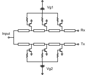
Figure 4 is the complete schematic of the SPDT traveling- wave switch. Two SPST switches and quarter wave-length transformers are included. Due to the different requirements in the transmit and receive paths, the switch design is designed to be asymmetric. Because of the parasitic resistance and capacitance of the transistors in on/off states, there are trade-offs between the insertion loss and isolation. In the receive path, the insertion loss is more important so the small devices are selected. On the other hand, the large devices are used in the transmit path for high power handling capability. In this design, the transistor size is 12 µm for the receive path, and 36
µm for transmit path. The BSIM3 model for the circuit simulation is provided by the foundry.
substrate
Metal 8
Metal 1
H 5.5 µm
ε
r 4.2Fig. 2. The structure diagram of thin film line in 0.13µm CMOS process. Frequency (GHz) 0 20 40 60 80 100 -0.5 -0.4 -0.3 -0.2 -0.1 0 Ins er tion lo ss ( dB)
Fig. 3. Simulated insertion loss of the thin film line with line width of 10 µm and length of 300 µm.
Input Rx
Tx Vg1
Vg2
Fig. 4. Traveling-wave switch schematic.
IV.MEASUREMENT RESULTS
The die photograph of this CMOS traveling-wave SPDT switch using 0.13-µm CMOS process is shown in Fig. 5. The chip size is only 0.8 x 0.5 mm2, which is the smallest switch designed using traveling-wave concept.
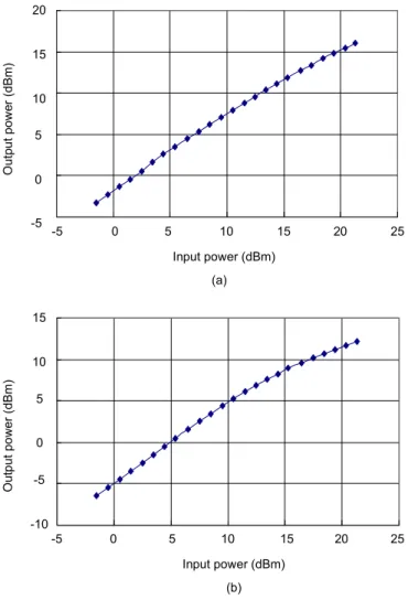
The circuit was tested via on-wafer probing. Figure 6 illustrates the measured and simulated insertion loss and isolation of the switch in the receive path. The SPDT switch achieves an insertion loss of 2.7 dB and an isolation of 26 dB from 27 to 50 GHz in the receive path. Figure 7 presents the measured and simulated insertion loss and isolation of the switch in the transmit path. It also achieves an insertion loss of 4.4 dB and an isolation of 14 dB from 30 to 63 GHz in the transmit path. The measurements agree with the simulation results well. Figure 8(a) shows Pout v.s. Pin of the switch in the receive path measured from Rx port to antenna port. When the dc bias of the Tx and Rx nodes is 0 V, and Vg1 and Vg2 is 0 and 1.2 V respectively, the switch achieves a P1dB of 11.5 dBm at 40 GHz. In the transmit path, when the dc bias of the Tx and Rx nodes is 0 V, and Vg1 and Vg2 is 1.2 and 0 V respectively, the switch achieves a P1dB of 13.8 dBm at 40 GHz measured from Tx port to antenna port as shown in Fig. 8 (b). Table Ι summaries the measured switch performances in transmit and receive paths.
Fig. 5. Die photo of the SPDT CMOS switch. The chip size is only 0.4 mm2. 0 10 20 30 40 50 60 70 80 Frequency (GHz) -50 -40 -30 -20 -10 0 Insertio n loss and isolation (dB) simulated measured Insertion loss isolation
Fig. 6. Measured and simulated insertion loss and isolation of the switch in the receive path.
0 10 20 30 40 50 60 70 80 Frequency (GHz) -30 -20 -10 0 simulated measured Insertion loss isolation Inser tion l oss and i sol at ion ( dB)
Fig. 7. Measured and simulated insertion loss and isolation of the switch in the transmit path.
TABLE I
SUMMARY OF MEASURED SWITCH PERFORMANCE IN TRANSMIT AND RECEIVE PATHS.
Rx path Tx path
Frequency (GHz) 27-50 30-63
Insertion loss (dB) 2.7 4.4
Isolation (dB) 26 14
-5 0 5 10 15 20 -5 0 5 10 15 20 25 Input power (dBm) (a) Out put pow er (dBm ) -10 -5 0 5 10 15 -5 0 5 10 15 20 25 Input power (dBm) (b) Out put pow er (dBm )
Fig. 8. Measured Pout v.s. Pin of the switch in the (a) receive path, and (b) transmit path. The input P1dB is 11.5 and 13.8 dBm in the receive and transmit paths, respectively.
V.CONCLUSION
Using 0.13-µm CMOS technology, a SPDT switch has been designed, fabricated, and tested. Using traveling-wave technique, it accomplishes the wide frequency range with smallest chip size. This MMIC switch operates from 27 to 50 GHz in the receive path, and from 30 to 63 GHz in the transmit path. At 40 GHz, a measured P1dB of 13.8 dBm in the transmit path is attained. The operation frequency range of the switch is the widest in CMOS process. Since the switch was fabricated using standard bulk 0.13-µm CMOS technology, it can be easily integrated with other front-end circuits to built CMOS transceivers without requiring any additional mask or post-processing steps.
ACKNOWLEDGEMENT
This work is supported in part by NTU-TSMC Joint-Development Project and National Science Council of Taiwan R.O.C. (NSC 93-2752-E-002-002-PAE, NSC 93-2219-E-002-016, NSC 93-2219-E-002-024 and NSC 93-2213-E-002-033).
REFERENCES
[1] Feng-Jung Huang and Kenneth O, “A 0.5-µm CMOS T/R switch for 900-MHz wireless applications,” IEEE J.
Solid-State Circuits, vol. 36, pp. 486-492, May 2000.
[2] Aruna Ajjikuttira,Chester Lrung, Ee-Sze Khoo, Mark Choke, Rajinder Singh, “A fully-integrated CMOS RFIC bluetooth application,” IEEE ISSCC2001 Dig. Tech. Papers, pp. 198-199. [3] Kenneth K.O, Xi Li, Feng-Jung Huang, and William Foley,
“CMOS components for 802.11b wireless LAN applications,”
IEEE RFIC Symp., pp.103-106, 2002.
[4] M. Madihian, L. Desclos, T. Drenski, “CMOS RF ICs for 900MHz-2.4GHz band wireless communication networks,”
IEEE RFIC Symp., pp. 13-16, 1999.
[5] Niranjan Talwalkar, C Patrick Yue, and S. Simon Wong, “An integrated 5.2GHz CMOS T/R switch with LC-tuned substrate bias,” IEEE ISSCC2003 Dig. Tech. Papers, pp. 362-363, 2003. [6] K.-Y. Lin, W.-H. Tu, P.-Y. Chen, H.-Y. Chang, H. Wang, and
R.-B. Wu, “Millimeter-wave MMIC passive HEMT switches using traveling-wave concept,” IEEE trans. Microwave Theory
and Tech., vol. 52, issue 8, Aug. 2004.
[7] M. J. Schindler, and A. Morris, “DC-40 GHz and 20-40 GHz MMIC SPDT switches,” IEEE Trans. on Microwave Theory and
Tech., vol. MTT-35, no. 12 pp. 1486-1493, Dec. 1987.
[8] S. F. Chang, and W.-L. Chen, J.-L. Chen, W. Kung, and H.-Z. Hsu, “New millimeter-wave MMIC switch design using the image-filter synthesis method,” IEEE Microwave and Wireless
Component Lett., vol. 14, no. 3, pp. 103-105, March 2004.
[9] J. Kim, W. Ko, S.-H. Kim, J. Jeong, and Y. Kwon, “A high-performance 40–85 GHz MMIC SPDT switch using FET-integrated transmission line structure,” IEEE Microwave and
Wireless Component Lett., vol. 13, no. 12, pp. 505-507, Dec.
2003.
[10] D. Nayak, L.-T. Hwang, and I. Turlik, ‘‘Simulation and design of lossy transmission lines in a thin-film multichip package,’’
IEEE Trans. on Components, Packaging, and Manufacturing Technology, vol. 13, pp. 294-302, issue 2, June 1990.