國
立
交
通
大
學
光電工程學系碩士班
碩
士
論
文
銅銦鎵硒薄膜太陽能電池中化學水浴法製備
之硫化鋅緩衝層製程技術優化
The Zinc Sulfide Buffer Layer Fabrication
Using Chemical Bath Deposition Processes in
Cu(In,Ga)Se
2Thin Film Solar cells
研 究 生:白 諭
指導教授:謝漢萍 教授
黃乙白 副教授
銅銦鎵硒薄膜太陽能電池中化學水浴法製備之硫化鋅
緩衝層製程技術優化
The Zinc Sulfide buffer layer fabrication using chemical bath deposition
processes in Cu(In,Ga)Se
2thin film solar cells
研 究 生:白 諭 Student:Che-Hsuan Yang
指導教授:謝漢萍 Advisor:Han-Ping D. Shieh
黃乙白 Yi-Pai Huang
國 立 交 通 大 學
光 電 工 程 學 系 碩 士 班
碩 士 論 文
A ThesisSubmitted to Department of Electro-Optical Engineering College of Electrical and Computer Engineering
National Chiao Tung University in partial Fulfillment of the Requirements
for the Degree of Master
in
Electro-Optical Engineering July 2012
Hsinchu, Taiwan, Republic of China
i
銅銦鎵硒薄膜太陽能電池中化學水浴法製備之
硫化鋅緩衝層製程技術優化
學生:白諭 指導教授:謝漢萍教授
黃乙白副教授
國立交通大學電機學院 光電工程學系碩士班
摘 要
銅銦鎵硒是一種具有潛力的薄漠太陽能電池材料,目前其最高轉換效率達到 20.3%。然而在高效率太陽能電池的生產過程中,其緩衝層材料所使用的硫化鎘 由於包含了鎘的成分,在電池年限到達之後將會對環境造成汙染。因此本論文提 出對環境影響較小,同時不會嚴重降低電池效率的緩衝材料硫化鋅。由於硫化鋅 本身是活性較低的材料,不容易在銅銦鎵硒吸收層上形成高覆蓋率與適當鋅硫化 學當量比的薄膜,因此本論文針對化學水浴法製備之硫化鋅緩衝層做研究,包含 了薄膜覆蓋率、鋅與硫化學當量比、薄膜厚度三者的改善。論文中首先研究了溶 液中的溫度、氨水濃度、沉積時間對薄膜品質的影響,經由分析硫化鋅在化學水 浴法中的沉膜機制後,提出了兩種增進成膜品質的方法,分別為「後處理製程」 與「兩階段製程」。進一步研究「後處理製程」與「兩階段製程」發現兩階段製 程可以有效增進硫化鋅的成膜品質,硫化鋅的兩階段製程在銅銦鎵硒吸收層上只 需沉積大約 100 奈米的薄膜厚度即可達到了超過 95 %的薄膜覆蓋率、1.78 鋅與 硫化學當量比。ii
The Zinc Sulfide buffer layer fabrication using chemical bath
deposition processes in Cu(In,Ga)Se
2thin film solar cells
Student: Ian Pai Advisor: Prof. Han-Ping D. Shieh Prof. Yi-Pai Huang
Dept. of Photonics & Institute of Electro-Optical Engineering National Chiao Tung University
Abstract
Thin film Copper Indium Gallium Diselenide CIGS (CIGS) solar cells are one of
the most promising candidates. Until now, the latest world record CIGS solar cell has
achieved 20.3 % in efficiency. However, in CIGS solar cells fabrication, the use of
cadmium sulfide as buffer layer in CIGS solar cells contaminates the environments
when the solar cell panels reach lifetime. Therefore, the buffer material zinc sulfide
(ZnS) which rarely affects the environments and does not decrease the cell efficiency
largely was studied in this thesis. ZnS is a low activation material, so it is difficult to
deposit high coverage and suitable stoichiometric ratio ZnS thin-film on CIGS
iii
the ZnS buffer layer to reach desired Zn/S stoichiometric ratio and to improve
coverage properties by using chemical bath deposition (CBD). Firstly, the temperature,
the ammonia concentration, and the deposition time in chemical bath solution were
investigated on the film properties. By analyzing the ZnS film growth mechanism in
CBD method, two deposition methods, post-deposition and two-step deposition, are
proposed. Through further investigation of the post-deposition and the two-step
deposition, the two-step deposition method improves the ZnS film properties
effectively. The ZnS film deposited by two-step deposition only needs to deposit
about 100 nm thickness and then can reach over 95 % coverage properties and 1.78
iv
誌 謝
首先最誠摯感謝實驗室的兩位大家長:謝漢萍老師與黃乙白老師,兩位老師 在研究、態度、和報告上的指導與培養,使我在碩士生涯中能夠學習到不少的研 究知識、上台報告的技巧與做事情的態度,此外要感謝兩位老師提供豐富的資源 與完善的研究環境,讓此論文得以順利完成。另外,更要感謝每位口試委員所提 供的寶貴意見,使得本論文更加完善。 此篇論文能夠順利完成要特別感謝蔡柏全學長、王奕智學長與蔡韻竹學姊的 指導。兩年來,三位學長姐一路引導、協助並且鼓勵我,讓我在學術上或是生活 上學習到很多觀念與方法,讓我在碩士階段成長了不少。也要感謝同組的學長姐 們,濟宇以及子寬,在這兩年來的指導與協助,當我有問題時不吝惜的給我幫助 及建議。 兩年的研究生活,感謝大頭哥哥,致維哥、芳正、志明、台翔、精益、國振 等學長姐們提供各方面的指導與分享,也謝謝小馬、思頤、小頭、小董、馬爺、 博六、博詮、立偉、小 fighter,讓我的生活更加精彩。感謝拉拉、博凱、囧務 陪我度過了很多難熬的時刻,另外還有博鈞、上翰、秉彥、柏皓、岡儒陪我一起 留下了美好且精彩的回憶。和你們在課業、研究與生活上的討論與分享讓我又有 了不同的想法與開心的心情。也感謝米克、阿昌、小岡、小靖、登曜、小黑與雍 仁等學弟們在諸多事情上的幫助。再來還要謝謝助理姐姐們,雅惠、穎佳、茉莉、 蓮芳在各方面事情的處理上盡了很多心力,讓我們毫無後顧之憂也讓實驗室充滿 了歡樂的氣氛。 最重要的,我要感謝我最親愛的家人,謝謝爸媽的支持與鼓勵和妹妹的關 心,讓我在求學路程上可以毫無顧慮的專注在學習的部分。最後,我要將這份喜 悅分享給一路走來支持我的各位。v
Table of Contents
摘要 ... i
Abstract ... ii
誌 謝 ... iv
Table of Contents ... v
Figure Captions ... vii
Table Captions ... x
Chapter 1 Introduction ... 1
1.1 Solar Energy Background ... 1
1.2 CIGS Thin Film Solar Cells ... 5
1.3 CIGS Solar Cells Buffer Layer ... 6
1.4 Motivation ... 9
1.5 Organization ... 10
Chapter 2 CIGS Solar Cells ... 11
2.1 Principle of Photovoltaic Effect ... 11
2.2 CIGS Fabrication in each layer ... 15
2.2.1 Substrate ... 15
2.2.2 Back Contact Layer... 15
2.2.3 CIGS Absorber Layer ... 16
2.2.4 Buffer Layer ... 19 2.2.5 Window Layer ... 19 2.3 Fabricating Technique ... 21 2.3.1 Sputtering System ... 21 2.3.2 Evaporation System ... 22 2.3.3 Annealing Process ... 23
2.3.4 Chemical Bath Deposition ... 24
Chapter 3 Experiment ... 28
3.1 CIGS Deposition System ... 28
3.2 The Process of CIGS Fabrication ... 31
vi
3.2.2 Back Contact Metal Deposition ... 32
3.2.3 CIGS Absorber Deposition ... 32
3.2.4 Chemical Bath Deposition ... 33
3.3 Analytical Technologies ... 35
3.3.1 Scanning Electron Microscopy (SEM) ... 35
3.3.2 Energy Dispersive X-ray Spectroscopy (EDX) ... 37
3.3.3 UV-VIS Spectrometer ... 37
3.3.4 MATLAB Coverage Analysis ... 39
Chapter 4 Results and Discussion ... 41
4.1 Basic Characteristics ... 41 4.1.1 Temperature ... 41 4.1.2 Ammonia Concentration ... 43 4.1.3 Deposition Time ... 44 4.1.4 Summary ... 48 4.2 Deposition Improvements ... 48 4.2.1 Post-deposition ... 48 4.2.2 Two-step Deposition ... 53 4.2.3 Summary ... 63 4.3 ZnS Deposited on CIGS... 63
Chapter 5 Conclusions and Future works ... 66
5.1 Conclusions ... 66
5.2 Future Works ... 67
vii
Figure Captions
Fig. 1 The prediction of energy usage in the world ... 2
Fig. 2 Absorption coefficients of various semiconductor materials ... 3
Fig. 3 The structure of latest world record CIGS solar cells [5] ... 5
Fig. 4 Comparison of relative QE between CBD-ZnS and CBD-CdS ... 8
Fig. 5 Schematic of photovoltaic effect in semiconductors ... 12
Fig. 6 Current voltage characteristic of the solar cell ... 13
Fig. 7 Schematic of (a) co-evaporation principle and (b) cavity structure
... 17
Fig. 8 Three-stage process: 1
ststage: In, Ga, and Se co-evaporation at 350
, 2
ndstage: Cu and Se co-evaporation at 550
, and 3
rdstage: In,
Ga, and Se co-evaporation at 550
... 17
Fig. 9 Reaction process of (a) Se/H
2Se vapor, (b) Se solid layer, and (c)
CIGS formation ... 18
Fig. 10 The shunt-path prevention by sputtering i-ZnO layer ... 20
Fig. 11 Schematic of sputtering system ... 21
Fig. 12 Schematic of evaporation system ... 23
Fig. 13 Schematic of annealing system ... 24
Fig. 14 Schematic of mechanisms (a) Ion by ion collision and (b) Cluster
reaction ... 25
Fig. 15 Comparison of common products in CBD ... 27
Fig. 16 Schematic of CIGS deposition system in NCTU ... 28
Fig. 17 Photograph of the sputtering system ... 29
Fig. 18 Photograph of the selenization system ... 29
Fig. 19 Schematic of SEM system ... 36
Fig. 20 SEM in NCTU ... 36
Fig. 21 Energy transitions between different binding orbitals ... 38
Fig. 22 UV-VIS Spectrometer in NCTU ... 39
Fig. 23 A schematic of the SEM results of ZnS surface morphology ... 39
Fig. 24 A schematic after image processing ... 40
Fig. 25 The SEM results of ZnS surface morphology deposited at (a) 70
and (b) 80
... 42
Fig. 26 The SEM results of ZnS surface morphology deposited at (a) 2 M
viii
and (b) 4 M in ammonia mole concentration ... 43
Fig. 27 The SEM results of ZnS surface morphology deposited for (a) 10
minutes, (b) 20 minutes, (c) 30 minutes, (d) 40 minutes, and (e) 50
minutes ... 45
Fig. 28 The relationship between deposition time and the thickness of five
ZnS films ... 47
Fig. 29 The relationship between deposition time and the Zn/S ratio of
five ZnS films... 47
Fig. 30 The SEM results of ZnS surface morphology (a) without
post-deposition, (b) under ammonia post-deposition, and (c) under
thiourea post-deposition ... 50
Fig. 31 The SEM results of ZnS surface morphology (a) without
post-deposition, (b) post-deposited for 10 minutes, and (c)
post-deposited for 20 minutes ... 52
Fig. 32 The SEM results of ZnS surface morphology deposited for 20
minutes in first-step deposition (a) without further deposition, (b)
further deposited for 10 minutes, (c) further deposited for 20 minutes,
and (d) further deposited for 30 minutes ... 54
Fig. 33 The SEM results of ZnS surface morphology deposited for 30
minutes in first-step deposition (a) without further deposition, (b)
further deposited for 10 minutes, (c) further deposited for 20 minutes,
and (d) further deposited for 30 minutes ... 55
Fig. 34 The SEM results of ZnS surface morphology deposited for 40
minutes in first-step deposition (a) without further deposition, (b)
further deposited for 10 minutes, (c) further deposited for 20 minutes,
and (d) further deposited for 30 minutes ... 56
Fig. 35 The SEM cross-section results of ZnS surface morphology of (a)
Fig. 32-(d), (b) Fig. 33-(d), and (c) Fig. 34-(d) ... 57
Fig. 36 The relationship between deposition time and the coverage
properties of each deposition condition ... 60
Fig. 37 The relationship between the Zn/S ratio and second-step
deposition of each film ... 61
Fig. 38 The transmittance of (a) (20, 30) film, (b) (30, 30) film, and (c)
(40, 30) film ... 62
Fig. 39 The SEM top-view result of the ZnS surface morphology
deposited on CIGS/Mo/SLG substrate ... 64
Fig. 39 The SEM cross-section result of the ZnS surface morphology
ix
Fig. 41 The band diagram of (a) without band-gap modulation and (b)
with band-gap modulation ... 67
x
Table Captions
Table 1 Comparisons of CIGS solar cells in cell fabrication ... 6
Table 2 Comparisons of three buffer materials ... 9
Table 3 The performance characteristics in three kinds of solar cells ... 14
Table 4 The K
sp(RT) of several materials [28]... 27
Table 5 The compositions of CBD solution ... 34
Table 6 The hydrolysis reaction and main reaction equations in CBD .... 34
Table 7 The EDX results of ZnS deposited at (a) 70
and (b) 80
.. 42
Table 8 The EDX results of ZnS deposited at (a) 2 M and ... 44
Table 9 The EDX results of ZnS deposited for (a) 10 minutes, (b) 20
minutes, (c) 30 minutes, (d) 40 minutes, and (e) 50 minutes ... 46
Table 10 The EDX results of ZnS (a) without post-deposition, (b)
ammonia post-deposition (c) thiourea post-deposition... 50
Table 11 The EDX results of ZnS (a) without post-deposition, (b)
post-deposition for 10 minutes, and (c) post-deposition for 20
minutes ... 52
Table 12 The EDX results of ZnS deposited for 20 minutes in first-step
deposition, and then (a) without further deposition, (b) further
deposited for 10 minutes, (c) further deposited for 20 minutes, and (d)
further deposited for 30 minutes ... 58
Table 13 The EDX results of ZnS deposited for 30 minutes in first-step
deposition, and then (a) without further deposition, (b) further
deposited for 10 minutes, (c) further deposited for 20 minutes, and (d)
further deposited for 30 minutes ... 58
Table 14 The EDX results of ZnS deposited for 40 minutes in first-step
deposition, and then (a) without further deposition, (b) further
deposited for 10 minutes, (c) further deposited for 20 minutes, and (d)
further deposited for 30 minutes ... 59
1
Chapter 1 Introduction
Energy resources like oil, gas, and coal are mainly used in recent decades, but
the cost has gradually become high due to the limited energy resources on Earth. In
addition, when these fossil fuels are consumed, carbon dioxide from the production
process causes the Earth's greenhouse, melting glaciers, and climate anomalies.
Therefore, for natural environments, clean, renewable, and sustainable energy is
indispensable.
1.1 Solar Energy Background
As the development of science and technology continues, the consumption of
energy significantly increases. The reverses of the energy resources such as oil, gas,
and coal are limited on Earth and will be depleted one day in the future, so the
development of renewable energy has risen progressively. The prediction of energy
usage in the world is demonstrated in Fig. 1. So far in 2012, oil, gas, and coal are the
major supply for the energy used. Accompanying with the reduction of oil, gas, and
coal, renewable energy such as biomass, wind, and solar energy has become more
important. Among these renewable energy resources, solar energy is believed to
become a major power generation in the future because of its unlimited, pollution-free,
and wide-spread characteristics. However, solar energy has some issues such as
instability under different weather condition and high installation cost. Thus, many
research institutions and industries have been working on improving the conversion
2
So far, the classification of solar cells can be divided into three categories: (1) the
first generation: wafer-based solar cells, (2) the second generation: thin film solar
cells, and (3) the third generation: organic and nanotechnology solar cells. The
following is detailed description of each generation.
Silicon wafers were widely used in the semiconductor industry. Building on the
experience of the semiconductor industry, the manufacturing technologies of
wafer-based solar cells were already quite mature. Wafer-based solar cells included
single-crystalline and multi-crystalline solar cells. Single-crystalline solar cells which
had high cost and complex fabrication process achieved around 25% [1] in efficiency.
In contrast, multi-crystalline solar cells were proposed and reached about 20% [2] in
efficiency because of the lower cost and simplified fabrication process compared with
single-crystalline solar cells. Nevertheless, some issues from wafer-based solar cells
had to be concerned, including high cost, indirect band-gap, and low absorption
coefficient properties.
3
Unlike the first-generation solar cells, the second generation solar cells were
developed to improve the cell efficiency by selecting different materials. The
materials like copper indium diselenide (CIS or CuInSe2), cadmium telluride (CdTe),
and hydrogenated amorphous silicon (a-Si:H) were selected (as shown in Fig. 2)
because of their high optical absorption coefficient and thin material usage which was
enough to absorb most sunlight effectively. Generally, the second generation solar
cells were also called thin film solar cells. Moreover, in thin film solar cells, the reduced usage of materials was adapted to combine with inexpensive substrates such
as glass, flexible plastic, and stainless steel for decreasing the cost.
The third generation solar cells could be divided into two types: macromolecule
solar cells and organic solar cells. Both types had the advantages such as low cost,
simple production, and wide application. In addition, the portable and foldable
4
characteristics in macromolecule and organic solar cells could be used in cell phones,
clothing, backpacks, tents, and many daily necessities.
Among three generations, the second generation solar cells is preferred because
of its low cost compared to the first generation solar cells and its mature technology
compared to the third generation solar cells. In the second generation solar cells, CIS, CdTe, and a-Si:H are the high optical absorption compounds. Many researchers have
dedicated to optimize the fabrication of the aforementioned compounds for achieving
high conversion efficiency. CIS material shows relatively high absorptivity among
these materials as shown in Fig. 2. Almost the entire incident light is absorbed within
the first micrometer of the CIS film. Furthermore, the band-gap of CIS compound can
be dominated between 1.0 and 1.7 eV by doping small amounts of Gallium (Ga) into
the CIS film to form copper indium gallium diselenide (CIGS), which further
increases the absorption of sunlight.
For the cell efficiency in laboratory and module efficiency in corporation of the
present investigation, CIGS solar cells are 20.3% (0.503 cm2) and 15.7% (9703 cm2), CdTe solar cells are 16.7% (1.032 cm2) and 12.8% (6687 cm2),as well as a-Si:H solar
cells are 12.5% (0.27 cm2) and 10.4% (905 cm2) [3], respectively. The results
demonstrate the efficiency of CIGS is the best of three thin film materials. Besides the
efficiencies of solar cells, a material which is harmful to the environment should be
discussed. For CdTe, Cadmium (Cd) causes environmental pollution during the
manufactory as well as the problem of how to deal with contaminants when the solar
cell panels reach lifetime.
To summarize the above factors, CIS or CIGS has the potential to be the new
candidate in solar cells materials for its low production cost, high conversion
5
1.2 CIGS Thin Film Solar Cells
The first CIS photovoltaic device appeared in 1973 when a research team at
Salford University annealed CuInSe2 in indium [4]. So far, CIGS solar cells have
reached 20.3% in efficiency [5] at the size of laboratory-scale by Zentrum fuer
Sonnenenergie und Wasserstoff-Forschung (ZSW), in Baden-Wuerttemberg, Germany.
The cells setup of each layer can be described as following: soda-lime glass (SLG) as
a substrate, sputtered molybdenum (Mo) as back contact metal, co-evaporated CIGS
as absorber layer, chemical bath deposited cadmium sulfide (CdS) as buffer layer,
sputtered intrinsic zinc oxide (i-ZnO) and sputtered aluminum-doped ZnO (ZnO:Al)
as window layer, sputtered surface-structural MgF2 as anti-reflection layer, and a
nickel (Ni)/aluminum (Al)-grid as front contact. A schematic of CIGS thin film solar
cells from ZSW is demonstrated in Fig. 3.
Prof. Ingvid Repius, National Renewable Energy Lab (NREL), USA, provided
the similar cell fabrication, and the cell efficiency achieved 19.9% [6]. Prof. Tokio
6
Nakada from Aoyama Gakuin University (AGU), Japan, proposed the CIGS solar cell
with the toxic-free buffer material zinc sulfide (ZnS), and the cell efficiency achieved
18.6% [7]. The simple comparisons of CIGS solar cells fabricated by these three
research institutions are listed in Table 1.
Table 1 Comparisons of CIGS solar cells in cell fabrication
MBE*: Molecular beam epitaxy.
1.3 CIGS Solar Cells Buffer Layer
Buffer layer is indispensable in high-efficient CIGS thin-film solar cells. The
functions of buffer layer are listed below.
1) Match band-gap between window layer and absorber layer 2) Protect absorber layer from ion bombardment
3) Provide the p-n junctions
In CIGS solar cells, ZnO is commonly used as window materials. The band-gap
of ZnO is about 3.2 eV, and the band-gap of CIGS absorber layer is about 1.0 to 1.7
eV. If the ZnO is deposited on CIGS, the large band offset in CIGS/ZnO interface may
cause severe carriers’ recombination which can dramatically decrease cell efficiency. In order to reduce the carriers’ recombination, the addition of the CdS as buffer layer
is needed. Institutes CIGS deposition Buffer material Window layer Efficiency (%)
ZSW Co-evaporation CdS ZnO, ZnO:Al 20.3 [5]
NREL Co-evaporation CdS ZnO 19.9 [6]
7
Buffer layer can protect absorber layer from the damage by sputtering which is
the most applied technique in depositing window layer ZnO. During the sputtering,
strong-energy argon (Ar) plasma ions will destroy the surface of CIGS absorber layer
by ion bombardment. Therefore, the addition of buffer layer is used to protect the
surface of absorber layer.
The formation of p-n junctions is important in solar cells. When electrons in
solar cells are excited under the illumination, these electrons will be driven to the
electrodes by the build-in electric field caused by p-n junctions. The purpose of buffer
layer is to yield the n-type semiconductor accompanying with the p-type CIGS.
High-active CdS is commonly utilized in high-efficient CIGS solar cells because
CdS can achieve thin and high-coverage film. The band-gap of CdS is about 2.4 eV
which means CdS can also provide desirable matching between ZnO and CIGS.
However, optical loss by the wavelength below 520 nm of sunlight from lower
band-gap and Cd toxicity are the issues. Therefore, the investigation of Cd-free buffer
materials with higher band-gap is recommended.
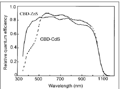
Showa Shell investigated ZnS deposited by chemical bath deposition (CBD)
method as Cd-free buffer materials, as well as the cells efficiency in module achieved
12.5% [8-9]. CBD-ZnS has higher optical transmission in short wavelength regions of
sunlight because the band-gap of CBD-ZnS is much larger than the band-gap of
CBD-CdS. The quantum efficiency (QE) of CBD-ZnS and CBD-CdS compared by
Nakada Group is shown in Fig. 4 [10]. The quantum efficiency of CBD-ZnS below
8
Indium sulfide (In2S3) also provides the feasibility of replacing CdS. To obtain
high performance, In2S3 is fabricated by CBD and atomic layer deposition (ALD).
CBD-In2S3 deposited in CIGS solar cells by Prof. Dimitri Hariskos from ZSW
achieved 15.7% in efficiency [11]. Cells efficiency of In2S3 deposited with ALD on
CIGS by Prof. Naghavi from Centre National de Recherche Scientifique, Laboratoire
d'Electrochimie et de Chimie (LECA-CNRS), France, was 16.4% [12].
So far, although CBD-ZnS and ALD-In2S3 are still not competitive with
CBD-CdS, many research institutes and industries have dedicated to investigate ZnS
and In2S3 due to their potential of better optical transmission below the short-wavelength region and without the Cd utilization. The simple comparisons of
buffer materials fabricated by the three research institutions are listed in Table 2.
9
Table 2 Comparisons of three buffer materials
1.4 Motivation
CIGS is one of the potential materials for thin-film solar cells due to its high
absorption coefficient and direct band-gap, so many research institutes work for
bringing CIGS solar cells to mass production. During the fabrication, buffer layers
deposited on CIGS film by non-vacuum CBD were reported to show better
performance because CBD method could provide the benefits such as easy to scale-up,
low cost, and short processing time. Furthermore, consider of environmental issues,
optical transmittance, and performance in cells efficiency, the ZnS buffer layer
deposited by CBD method is preferred.
However, it is difficult to accurately control the compound reaction in CBD
method because CBD method is a non-vacuum process. The appearance of zinc
hydroxide (Zn(OH)2) in ZnS films cannot be avoided in CBD process. Also, the
relatively low activity of ZnS is hard to form thin and well-coverage films. Therefore, there are some issues in accomplishing the balance between stable fabrication process,
suitable stoichiometric ratio, well coverage properties, and thin-thickness in
CBD-ZnS. In this thesis, some methods will be proposed to improve these issues. Buffer material Deposition method Institutes Efficiency (%) Features CdS CBD ZSW 20.3 [5] High-efficiency ZnS CBD AGU 18.6 [7] QE response
10
1.5 Organization
In this thesis, “The zinc sulfide buffer layer fabrication using chemical bath
deposition processes in Cu(In,Ga)Se2 thin film solar cells” will be discussed. The
structure is shown as follows. The principle of photovoltaic effect, CIGS fabrication,
and the characteristics of fabricating technique are presented in Chapter 2. In
Chapter 3, the fabrication processes, the fabrication facilities, and the measurements are explained in detail. Results and discussions of ZnS films on the CIGS/Mo-coated
substrate are described in Chapter 4. Finally, the conclusion and future works are
11
Chapter 2 CIGS Solar Cells
The principle of photovoltaic effect in solar cells will be presented. Four
fabrication techniques will be introduced, including sputtering, thermal evaporation,
annealing, and chemical bath deposition.
2.1 Principle of Photovoltaic Effect
The concept of discrete portions of the light’s energy was firstly introduced by Max Planck and further confirmed by Albert Einstein who proposed that light can be
regard as the composition of packets of photons. The photon energy is equal
to the product of h and ν, where h is the Planck’s constant and ν is the frequency of light. The frequency ν ( ) is related to the wavelength λ (m) through the speed of light c (m/s) by and the relationship is written as equation 2-1 as shown
below.
The principle of solar cells was based on the photovoltaic effect and the effect
was proposed by Albert Einstein in 1939 [13]. In a semiconductor material, the
minimum energy required for generating a free electron is the energy , where
is the energy between the valence band and conduction band. When the
semiconductor material is illuminated, the material absorbs the incoming energy
which is larger than the band-gap of the semiconductor material. The photon energy
of an incoming photo excites an electron from the valence band to the conduction
band and leaves behind a hole in valence band. A schematic of photovoltaic effect in
the semiconductors under illumination is illustrated in Fig. 5.
12
When the p-n junctions formed by contacting the p-type and n-type
semiconductors is illuminated by incident light, the excited carriers are generated and
driven by the build-in electric field between p-n junctions. Eventually, the light
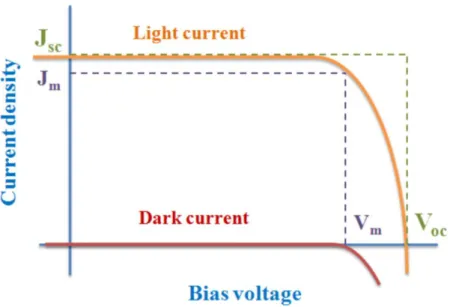
current will generate if the p-n junction is connected to an external circuit.
The generation of short circuit photocurrent is dependent on the incident photons.
The connection between short circuit photocurrent and incident photons is shown in
the following equation
Eq. 2-2
where is named as the short circuit current density, q is the electronic charge,
is the incident spectral photon flux density, and Q.E.(E) is the quantum
efficiency of incident photon carrying with energy E.
Except the photocurrent, there is another current delivers the opposite direction
to the photocurrent because the p-n junctions inside the semiconductor can be treated
as the p-n diode. This reverse current is called the dark current and it is developed by
the potential difference between the terminals of the diode. The dark current density
can be described in equation 2-3.
13
Eq. 2-3
Where is the reversed saturation current, q is the electronic charge, V is the
bias voltage without illumination, A is the ideality factor of diode which is decided by
materials, is Boltzmann’s constant, and T is absolute temperature (k).
Since the short circuit current and the dark current are in the opposite direction,
the net current density in the solar cells is defined as
Eq. 2-4
Bringing equation 2-3 into equation 2-4, equation 2-4 can be simplified to
Eq. 2-5
When is equal to zero, the open-circuit voltage can be obtained from
equation 2-5
Eq. 2-6
The current voltage characteristic of solar cell is illustrated in Fig. 6, the
operating region works in the range of and of solar
cell.
14
The power density P is the product of the current density J and the bias voltage V.
The maximum power density is defined by the product of the current density and
the bias voltage . The equation is given by
Eq. 2-7
The fill factor (FF) which is used for evaluating the performance of solar device
is defined in equation 2-8.
Eq. 2-8
The conversion efficiency of a solar device is further acquired by the
maximum power density over power density of the incident light.
Eq. 2-9
Apparently, the efficiency can be described by , , as well as FF. These
four characteristics η, Jsc, Voc, and FF are usually used for appearing the performance
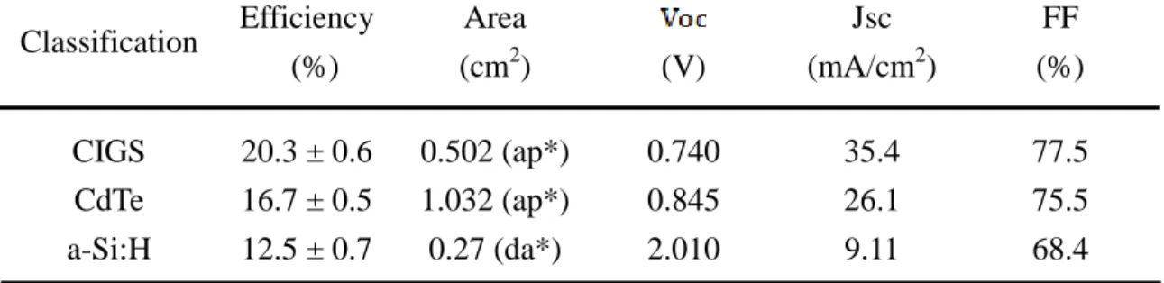
of solar cells. Typical values of the performance characteristics for the most advanced
CIGS and other thin-film solar cells are listed in Table 3 [3].
Table 3 The performance characteristics in three kinds of solar cells
ap*: aperture area
da*: designated illumination area
Classification Efficiency (%) Area (cm2) (V) Jsc (mA/cm2) FF (%) CIGS 20.3 ± 0.6 0.502 (ap*) 0.740 35.4 77.5 CdTe 16.7 ± 0.5 1.032 (ap*) 0.845 26.1 75.5 a-Si:H 12.5 ± 0.7 0.27 (da*) 2.010 9.11 68.4
15
2.2 CIGS Fabrication in each layer
2.2.1 Substrate
It is very important to choice substrates used in CIGS solar cells since the
substrates need to be stable during the fabrication. The substrates should be
chemically-inert from the selenization process and thermally-stable from the
high-temperature annealing in the range of 400 to 600 . So far, plate glass
substrates are adopted for the application.
Soda-lime glass is usually used as the substrates in CIGS solar cells because of
the feasible price and sodium (Na) diffusion from SLG to CIGS absorber layer, where
Na diffusion can improve the structural and electrical properties. It was reported that
the CIGS solar cells deposited on the SLG (Na = 0.1 at %) were found to have higher
conversion efficiencies than the one prepared on the borosilicate substrates [14-15].
2.2.2 Back Contact Layer
The back contact layer is the back electrode of the CIGS solar cells. Several
materials were reported to be the contact metal such as tungsten (W), molybdenum (Mo), and Titanium (Ti) [16-17]. Among the metals, Mo was chosen typically as back
metal contact. Mo, the historical back contact material for CIGS solar cells, achieved
well performance with most favorable electricity, optical properties, and the inertness
from the highly corrosive process. Sputtering is the common deposition technique for
Mo layer. To obtain the Mo film with low resistivity and good adhesion, two stacking
layers are applied by sputtering the first layer with good adhesion in high working
16
In addition, during the CIGS formation procedure at high temperature, Mo may
interact with active selenium (Se) to form an extremely thin molybdenum diselenide
(MoSe2) layer in the interface between Mo and CIGS. The formation of MoSe2 was
reported to benefit the solar device performance because the appearance of MoSe2
resulted in the ohmic contact which was favorable for current transferred [18-19].
Moreover, MoSe2 could improve the adhesion between CIGS and Mo [20].
2.2.3 CIGS Absorber Layer
CIGS absorber layer can be fabricated by both vacuum and non-vacuum
processes. In general, the absorber formed by vacuum processes reveals higher
efficiency than that of non-vacuum processes. The vacuum processes of the
co-evaporation method and the selenization process of precursors will be introduced
in the following.
Co-evaporation
Co-evaporation is the best method among the CIGS deposition techniques,
especially for laboratory-scale devices because of the flexibility of the Cu, In, Ga, and
Se flux in evaporation process. The latest world record of cells efficiency in CIGS
solar cells has achieved 20.3% by using this co-evaporation method. The typical
17
Fig. 7 Schematic of (a) co-evaporation principle and (b) cavity
structure
The most successful modification of the co-evaporation process was called
three-stage process as shown in Fig. 8 [21]. In the first stage, the sources of In, Ga,
and Se were evaporated simultaneously on the substrate heated at 350 . Then the
source of Cu and Se were evaporated in the second stage at 550 . At the end of the
three-stage process, the source of In, Ga, and Se were evaporated simultaneously
again at 550 to ensure the variations of the Ga/In and Cu/(In+Ga) ratio for graded
band-gap through the film [22-23].
Fig. 8 Three-stage process: 1
ststage: In, Ga, and Se co-evaporation
at 350
, 2
ndstage: Cu and Se co-evaporation at 550
, and 3
rd18
Even through the CIGS film fabricated by three-stage co-evaporation process is
realized with the smooth, dense, and well-controlled film, the capability for the
large-scale application in commercial use should be concerned due to the uniformity
through the module panel.
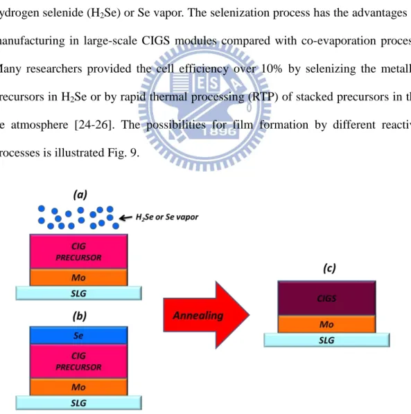
Selenization of Metallic Precursors
Selenization process with Cu-In-Ga (CIG) metallic precursor is another method
to fabricate CIGS thin film. The first step is to stack CIG precursor on Mo-coated
substrate and then the second step is to selenize the CIG precursor with the use of
hydrogen selenide (H2Se) or Se vapor. The selenization process has the advantages of
manufacturing in large-scale CIGS modules compared with co-evaporation process.
Many researchers provided the cell efficiency over 10% by selenizing the metallic
precursors in H2Se or by rapid thermal processing (RTP) of stacked precursors in the
Se atmosphere [24-26]. The possibilities for film formation by different reactive
processes is illustrated Fig. 9.
Fig. 9 Reaction process of (a) Se/H
2Se vapor, (b) Se solid layer, and
(c) CIGS formation
19
2.2.4 Buffer Layer
The buffer material acts as a matching layer both electrically and optically
between the absorber layer and window layer. So far, variety kinds of buffer materials
were investigated for the better performance and fabricated by either vacuum or
non-vacuum process.
The method to deposit the buffer layer on CIGS absorber layer is mainly
employed by non-vacuum CBD method in high-efficient solar cells. CBD method
were reported to show better performance than any other vacuum process methods
because CBD process can provide the benefits such as good film coverage, low cost,
and short processing time.
The CdS films deposited by CBD method are widely used as an interfacial layer
of the high efficiency CIGS thin-film solar cells. Recently, several research groups
report that the diffusion of Cd into the CIGS absorber can form buried p-n junctions
inside the absorber [27]. However, the used of Cd is concerned due to the
environment issues. Consider of environmental protection, thin film ZnS is preferred
as the substitution for CdS. The more detail about CBD-ZnS will be discussed in
Chapters 3 and 4.
2.2.5 Window Layer
Window layer, as the name implied, behaves as the function of the window for
the light passing through. The objectives of window layer in CIGS solar cells must
have:
1) The minimized light absorption
2) Low resistivity for carriers transportation
20
layer, the band-gap of the chosen materials should be relatively wider. To form
hetero-junctions, this window layer should contain n-doped materials. Transparent
conducting oxides (TCO) which are provided with well-conductivity and
high-transparent agree with the criteria. Indium tin oxide (ITO) is a well-known TCO
in flat-panel industries and solar technologies. However, the available ITO usage is
reduced due to the In limitation, so other alternatives are being studied. One of the
potential alternatives in CIGS solar devices is ZnO:Al because Al and ZnO are
easily-obtained on Earth.
An ordinary deposition technique for the window layer is fabricated by
sputtering. As shown in Fig. 10, before sputtering ZnO:Al window layer on buffer
layer, a high resistivity intrinsic ZnO (i-ZnO) was sputtered to prevent the shunt-path
from ZnO:Al to Mo. Other benefits like increasing open-circuit voltage and fill factor
of the device are also significantly dependent on involving the high resistivity i-ZnO
in CIGS solar devices.
Fig. 10 The shunt-path prevention by sputtering i-ZnO layer
Since this deposition of window layer is almost the last step in the CIGS solar cells
fabrication, the working power, pressure, and temperature during or after sputtering
21
2.3 Fabricating Technique
The fabrication techniques: sputtering system, thermal evaporation system, annealing process, and chemical bath deposition used in this thesis will be illustrated.
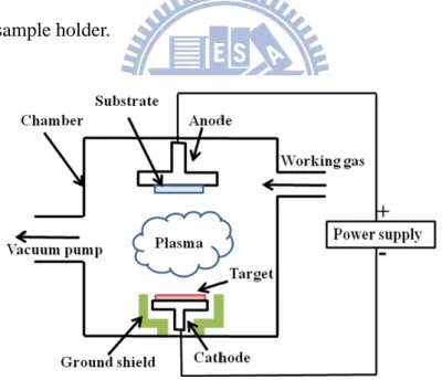
2.3.1 Sputtering System
Sputtering causes particles ejection by momentum transfer in the high vacuum
level ( Torr). The momentum transfer is caused by striking energetic
ions or neutral atoms on the surface of a solid target.
A schematic of the sputtering process is shown in Fig. 11. In general, sputtering
system consists of a power supply, vacuum atmosphere, working gas, vacuum pumps,
targets, and a sample holder.
In a typical sputtering process, the chamber is evacuated to high vacuum
atmosphere before sputtering. Then the Ar working gas flows into the chamber until
the working pressure in the chamber achieves Torr level. The target is then
biased by a direct current (DC) or radio frequency (RF) on negative electric potential
22
to produce the plasma between target and ground shield. The energetic ions in the
plasma sustain the glow-discharge situation. The positively charged ions are driven by
the potential gradient across the chamber and are accelerated to strike the surface of
the target to dislodge particles of the target. The ejected particles then travel through
the chamber and finally deposit onto the substrate.
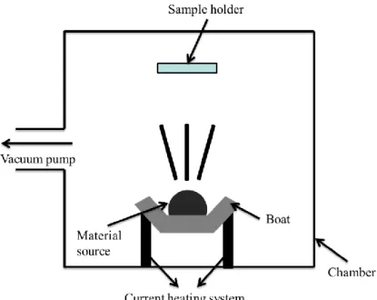
2.3.2 Evaporation System
The system of evaporation deposition is to heat a boat with material pellets to
sufficiently high temperature under vacuum so that particles are liberated from the
boat and the particles travel through the vacuum to deposit onto the substrate. This
method includes three characteristics:
1) The desirable materials transfer from solid phase to vapor phase 2) Transportation from source to substrate
3) Nucleation and growth of film on the sample surface
A schematic of evaporation system is shown in Fig. 12. The evaporation system
consists of a chamber, vacuum pumps, material sources, a heating system, and a
23
Fig. 12 Schematic of evaporation system
High vacuum in the chamber is required for reducing the residual gas impurity
levels, maximizing the molecule absorption rate onto the substrate surface, and
decreasing the amount of unnecessary gas phase collisions.
2.3.3 Annealing Process
Annealing is often applied in metallurgy or materials engineering fabrication
process. The purpose of annealing is to improve thin-film crystallization and release
the internal residual stress.
A schematic of annealing system is shown in Fig. 13. The annealing system
consists of a chamber, vacuum pumps, working gas, heating sources, and a sample
24
To enhance the crystalline structure after fabrication process, the annealing
process is required. Annealing process is a heating process containing three
temperature steps: heating, maintaining, and cooling. In the heating step, the
temperature must reach the materials recrystallization temperature. The temperature is
maintained for a period of time to provide energy for recrystallization and grain
growth. Cooling must be stable and slow to prevent the inherent-stress damage.
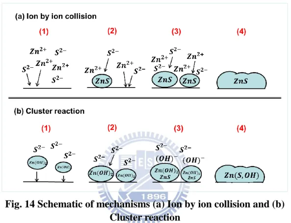
2.3.4 Chemical Bath Deposition
Chemical bath deposition, classified by the growth mechanism, can be divided
into two main types: ion by ion collision and cluster reaction. For the mechanism of
ion by ion growth, a high-degree of supersaturation is needed to nucleate. The
ion-by-ion mechanism introduces the heterogeneous nucleation right on the surface,
such as substrates or vessel walls, to form the films. Cluster reaction, also named as
hydroxide mechanism, is the nucleation of metal chalcogenide. In this mechanism, the
metal hydroxide film forms on the surface of substrates at the beginning, and then
hydroxyl is substituted by chalcogenide. The continuous of metal hydroxide
25
deposition and chalcogenide substitution create the buffer films.
The detail of both mechanisms is shown in Fig. 14, where the ZnS and Zn(OH)2
are employed to illustrate the growth mechanisms.
The ion-by-ion collision contains four steps as shown in Fig. 14 (a):
(1) S and Zn ions diffuse onto the substrate (2) The ZnS nuclei forms
(3) Growth and aggregation of the ZnS nuclei (4) ZnS forms as the film
The cluster reaction also includes four steps as shown in Fig. 14 (b):
(1) Diffusion of Zn(OH)2 colloids to the substrate (2) Zn(OH)2 colloids adhereto the substrate
Fig. 14 Schematic of mechanisms (a) Ion by ion collision and (b)
Cluster reaction
26
(3) Hydroxide is replaced by sulphide at the surface (4) The film Zn(S,OH) forms
Ammonia which provides the complex ions and hydroxyl is added in the CBD
process to control the amount of Zn ions by Zn-complexes and the pH value. By
adjusting the amount of Zn ions and the pH value, the rates of reaction can be
controlled to deposit favorable films.
During the deposition, the solution is heated by a heat plate connected with a
temperature controller which is to maintain the stationary temperature in the region of
60 to 90 . A magnetic bar is kept in stirring to retain the solution uniformity.
After the deposition, post-treatment like ultrasonic cleaning and baking of
deposited films is needed to enhance the film properties. The ultrasonic cleaning
removes the loose particles on the films surface and the baking eliminates the
moisture produced from aqueous solution.
The solubility product constant ( ) is an important factor in chemical bath
reaction. Consider the reaction of a compound AB dissolves in solution,
is defined as the product of a constant k, , and concentration in
equilibrium,
(equilibrium)
The constant k is relative to the absolute temperature. For a non-equilibrium reaction of the compound AB dissolves in solution, J is defined as the product of a constant k,
, and concentration in this non-equilibrium condition.
27
When J , the precipitation occurs. When J , the reaction is in
equilibrium. When J , the compound dissolves. The at room-temperature
of common products in CBD-CdS and CBD-ZnS are shown in Fig.15 and listed in
Table 4. Owing to a small value of the ZnS film, the deposition rate and the
growth mechanism of the thin film must be controlled by the complex agents such as
ammonia, hydrazine, and ethylenediamine tetra-acetate (EDTA).
Table 4 The K
sp(RT) of several materials [28]
Materials
K
sp(RT)
CdS
Cd(OH)
2ZnS
Zn(OH)
228
Chapter 3 Experiment
A deposition system in National Chiao-Tung University (NCTU) will be
illustrated, including a sputtering chamber, a selenization chamber, and an
experimental setup for fabricating the ZnS film on CIGS/Mo/SLG. Analytical
equipments such as scanning electron microscope (SEM), energy dispersive X-ray
spectrometer (EDX), UV-VIS spectrometer, and MATLAB Numerical Analysis will
be illustrated.
3.1 CIGS Deposition System
To deposit CIGS thin film, a self-designed CIGS deposition system was used in
this thesis. This deposition system consisted of a sputtering and a selenization
chamber. A load-lock chamber was connected between the sputtering and the
selenization chamber so that the sample could be maintained in a relatively clean
environment during the different fabrication process. A schematic of the CIGS
deposition system is shown in Fig. 16.
29
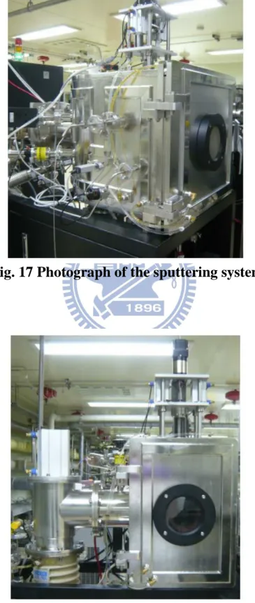
Photographs of the sputtering system and the selenization system are shown in
Figs. 17 and 18, respectively.
Fig. 17 Photograph of the sputtering system
30
In order to achieve the high vacuum level in the sputtering system, a mechanical
pump and a cryogenic pump were set up. The mechanical pump was an oil-sealed
rotary pump, which was used to establish the necessary fore-vacuum value for the
cryogenic pump. It could bring the pressure from atmosphere to around
Torr. Cryogenic pump was based on the principle of cold trap. Over several periods of
removal and entrapment by freezing the molecules on the cooled surface, the pressure
in the chamber was pumped down. In this system, the based vacuum was
Torr.
The 3-inch target with a smooth surface and symmetrical disk-shape were made
of the materials for the deposition. In this thesis, metallic targets like Mo, Cu, and In,
as well as compound targets like Cu-Ga, intrinsic ZnO, and ZnO:Al were used in cell
fabrication.
To attain a high vacuum level in selenization system, two pumps were used in
fabrication process: a rotary pump and a diffusion pump. Before launching the
evacuation for requisite vacuum level by the diffusion pump, the rotary pump was
served to assist the diffusion pump by constantly removing gas molecules. During the
operation of the diffusion pump, the oil was heated to around 200 which
percolated at high velocity through a series of baffle plates to remove gas molecules.
After the operation, the desirable high vacuum level was acquired. An issue has to be
concerned that the back streaming of oil from the heated diffusion pump may diffuse
into the processing chamber and contaminate the sample.
The selenization system was composed of the evaporation and annealing process
in the same chamber in order to retain the Se-vapor in annealing process. During the
annealing process, the retention Se-vapor would contribute to the CIGS grain growth.
In this thesis, Se pellets as the source were placed in a thermally heated tungsten
31
pressure of the source material in the gas phase had to be greater than in the solid
phase in order to deposit Se on the substrate.
After the evaporation of elemental Se on the metallic precursors, the annealing
process in the Se-containing atmosphere was applied in the same chamber and the
films were heated by halogen lamps. The annealing process with Se-vapor was a heat
treatment that involves three steps: heating, maintaining for a period, and cooling.
After the selenization process, the recrystallization of Cu-In-Ga precursor with Se
layer would form CIGS polycrystalline. The chemical as well as physical properties
of precursors might change after the conditions on selenization process such as
elemental diffusion.
3.2 The Process of CIGS Fabrication
In this section, the CIGS fabrication process will be introduced. The buffer
material ZnS deposited on SLG and CIGS/Mo/SLG substrates will be investigated.
3.2.1 Substrate Cleaning
In order to remove the undesired particles and contaminations on the SLG
substrate, the SLG is cleaned as follows:
(a) Clean the SLG substrate by deionized (DI) water
(b) Clean the SLG with detergent and then wash out the detergent
(c) Place the SLG on the teflon holder, and put the holder into a container with
acetone. Remove the organic contamination by the ultrasonic cleaning for 20
minutes.
(d) Place the SLG into another container with isopropanol (IPA). Remove
acetone by the ultrasonic cleaning in 20 minutes.
32
cleaning in 20 minutes.
(f) Use nitrogen jet to purge and dry the SLG.
(g) Put the SLG on a hot plate with 150 oC for 30 minutes to remove surface
moisture.
3.2.2 Back Contact Metal Deposition
The back contact metal Mo was deposited on the cleaned SLG substrate by DC
magnetron sputtering with thickness around 0.8 μm. The sputtering chamber was
pumped down to the base vacuum of Torr. The working pressures were set
to be between and Torr, and the powers of the sputtering gun
were set up between 50 and 150 W. During the sputtering, the sample holder rotated
with a rotating rate of 10 revolutions per minute (rpm).
3.2.3 CIGS Absorber Deposition
The preparation of CIGS absorber can be divided into two parts: deposition of
metallic precursors and selenization process.
Deposition of Metallic Precursors
The CIG precursors were deposited on the Mo-coated substrate by DC
magnetron sputtering. During the sputtering, the sputtering chamber was pumped
down to a base pressure of Torr. The chamber pressure was set to be
Torr by filing with Ar gas, and the power of the sputtering gun was set to
be 50 W on a 3-inch target. The sample holder rotated at a rotating rate of 10 rpm. The
deposition was started at room temperature.
The deposition of precursors was stacked in two ways: sequential and
33
deposition might affect the CIGS surface morphology, vertical composition, and the
crystalline quality of the films after selenization. In addition, to obtain the desirable
composition of film, the film deposition was accomplished by sequentially depositing
In thin layers and then simultaneously depositing Cu-Ga and In layers. The power
applied on Cu and Cu-Ga targets was adjusted while the power applied on In target
was fixed.
Selenization Process
To incorporate Se into the precursors, Se might be evaporated onto the surface of
precursors in advance and followed by an annealing process in the Se-containing
atmosphere. The selenization chamber was pumped down to a base vacuum of
Torr. During the selenization, the sample holder rotated at a rotating rate of 10 rpm.
The annealing temperatures were set between 350 and 550 .
Selenization was a key process that affects the resulting adhesion, composition,
orientation, and phase purity of films. Se was usually supplied excessively to assure
the complete formation of selenides (CIGS, In2Se3, or Cu2Se) with Cu-In-Ga
precursors since elemental Se might escape from surface of the sample due to the low
vaporization point of Se. Therefore, the flux of Se source for evaporation and the
annealing temperature should be carefully controlled.
3.2.4 Chemical Bath Deposition
To deposit ZnS films by CBD method in this thesis, the solution consisted of
zinc sulfate (ZnSO4) as a source of zinc (mole concentrations ranged from 0.02 M to
0.6 M) and thiourea (CS(NH2)2) as a source of sulfide (mole concentrations ranged
from 0.2 M to 0.8 M). Ammonia was added into the solution to provide an alkaline
34
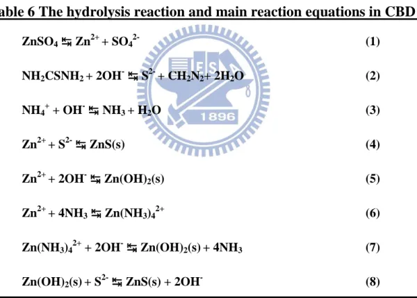
hydrolysis reaction of ZnSO4, CS(NH2)2, ammonia, and part of reaction equations are
listed in Tables 5 and 6, respectively.
Table 5 The compositions of CBD solution
ZnSO
4(M)
0.02 ~ 0.6
CS(NH
2)
2(M)
0.2 ~ 0.8
NH
3(M)
2 ~ 6
pH
9 ~ 11
Temp. ( )
60 ~ 90
Table 6 The hydrolysis reaction and main reaction equations in CBD
ZnSO4↹ Zn2+ + SO42- (1) NH2CSNH2 + 2OH-↹ S2- + CH2N2+ 2H2O (2) NH4+ + OH-↹ NH3 + H2O (3) Zn2+ + S2-↹ ZnS(s) (4) Zn2+ + 2OH-↹ Zn(OH)2(s) (5) Zn2+ + 4NH3 ↹ Zn(NH3)42+ (6) Zn(NH3)42+ + 2OH-↹ Zn(OH)2(s)+ 4NH3 (7) Zn(OH)2(s)+ S2-↹ ZnS(s) + 2OH- (8)
The solution temperature controlled by temperature controller was set up at 60 to
90 . A magnetic bar was kept in stirring to maintain the solution uniformity. To
investigate the ZnS films properties, ZnS was deposited on both SLG and
35
cleaning in deionized water to remove the loose ZnS particles on the film and then
baked at 150 in the air environment to eliminate the moisture produced from
aqueous solution.
3.3 Analytical Technologies
In this section, three analytical facilities will be presented, including SEM, EDX,
and UV-VIS spectrometer. Numerical analysis used to estimate coverage properties of
the film by MATLAB will be mentioned.
3.3.1 Scanning Electron Microscopy (SEM)
Scanning electron microscope (SEM) is a facility which can examine samples'
topography and morphology. Unlike the conventional optical microscope, SEM
utilizes electrons to reveal the image of the sample.
In SEM, there are two methods to generate electrons: thermionic and
field-emission. The generated electrons by thermionic or field-emission methods are
accelerated between a cathode and an anode and then the electrons are focused into a
small-diameter electron probe. Electric or magnetic fields, applied at right angles, can
be used to adjust the electrons direction for scanning the film surface. A schematic of
SEM system is illustrated in Fig. 19. Since the pressure in the sample chamber usually
amounts to about 10-4 Pa, the electron beam is allowed to travel from the cathode to
the sample with little interaction with the residual gas molecules.
When the accelerated high-energy electron beam bombards the sample, the
interaction between the electron beam and the sample generates a variety of responses,
including secondary electrons emission, back scattered electrons emission, x-ray
emission, and Auger electrons emission. By collecting and analyzing the resulted
36
Fig. 20 SEM in NCTU
Fig. 19 Schematic of SEM system
37
3.3.2 Energy Dispersive X-ray Spectroscopy (EDX)
Energy dispersive X-ray spectroscopy (EDX) is capable for identifying heavy
elements. The EDX technique is a specific technique used for the detection of the
characteristic X-ray. The emission of the characteristic X-ray is produced by
inner-shell excitation. The characteristic X-ray corresponds to each element because
each element has specific energy in inner-shell.
The identification of element from the emission of the characteristic X-ray is as
followed. After the generated characteristic X-ray transfers into a detector, the
detector converts the incoming X-ray photons into electron-hole pairs. The
electron-hole pairs are driven out of the detector and further converted to an electronic
pulse by a charge-sensitive preamplifier. The amplitude of the pulse is proportional to
the energy of the detected X-ray. A signal corresponding to the energy is processed
into the appropriate channel of a multi-channel analyzer. The signal processing
electronics calculates the number of pulses, resulting in a histogram of X-ray energy
versus intensity.
Furthermore, because of the X-ray absorption in the beryllium detector window
and in the lithium-drifted silicon chip, elements with atomic number less than ten are
not identified usually.
3.3.3 UV-VIS Spectrometer
UV-VIS spectrometer is the instrument used to analyze the sample responses to
different wavelengths of light, including reflection, transmittance, and absorption.
When an electron in molecule is under the light irradiation, the electron will absorb
the light energy. The specific light energy which results in electronic transitions in the
38
Qualitative measurement by UV-VIS spectrum can characterize the specific
wavelength absorption of each functional group because the specificity of functional
group. Molecular electronic binding orbitals are simply divided into three kinds; σ: single bond; π: double bond; n: not-binding electron pair. Several energy transitions are feasible such as σ→n, σ→σ*, n→π* and π→π* (as shown in Fig. 21). The energy required of n→π* and π→π* is fell in UV-VIS spectral range, so most applications are used in energy transitions n→π* and π→π*.
By measuring the difference of the initial incident light and the light interacted
with the sample, the spectrum from ultraviolet to visible can be determined. Before
the measurement in this UV-VIS spectrometer, the alto-zero process records the
reflection, transmittance, or absorption of substrates, so the effects by substrates can
be ignored during the analysis.
39
Fig. 22 UV-VIS Spectrometer in NCTU
3.3.4 MATLAB Coverage Analysis
In order to analyze the coverage properties of the ZnS surface morphology on the
SLG in SEM results, numerical analysis by MATLAB are used. A schematic of a
SEM result of ZnS surface morphology is shown in Fig. 23.
In Fig. 23, point A is located on the substrate. Point B, point C, and point D are
related to different particle size with different gray level. First, the gray level of point
A, point B, point C, and point D are defined as a’, b’, c’, and d’, respectively. In
40
general, the value of a’ is the smallest in the four number. Then, re-define the gray
level, the values in the figure larger than a’ correspond to black and the values in the
figure smaller than a’ correspond to white. The re-defined result is shown in Fig. 24.
By calculating the area of white and the area of black, the area of white is
obtained as W and the area of black is obtained as B. Finally, the film coverage
properties W/ (W+B) can be obtained. It shall be noted that the film coverage
properties by MATLAB numerical analysis is the estimation.
41
Chapter 4 Results and Discussion
4.1 Basic Characteristics
To achieve suitable stoichiometric ratio, well coverage, and thin-thickness ZnS film in chemical bath deposition, temperature, ammonia concentration, and deposition
time of chemical bath solution were investigated on the ZnS film properties.
Therefore, the influences of the temperature, the ammonia concentration, and the
deposition time in solution were investigated to optimize the ZnS film properties.
4.1.1 Temperature
From experimental experience data, the solution temperature selected over 90
was unsuitable because the solution boiled dramatically and became unstable for film
deposition. The boiling solution caused excessive reaction rate and undesirable
perturbation and then resulted in the poor ZnS formation. Otherwise, the solution
temperature below 60 was also unsuitable because of low reaction rate. Therefore,
the temperature should be set between 65 and 85 .
The ZnS deposition was performed with a solution consisting of 0.1 M ZnSO4,
0.4 M CS(NH2)2, and 6 M ammonia in concentration. The solution temperatures were
set to be 70 and 80 to determine the temperature effects on the depositing ZnS
films. The deposition time was 50 minutes in both temperatures. The SEM results of
42
(a)
(b)
Fig. 25 The SEM results of ZnS surface morphology deposited at (a)
70
and (b) 80
In Figs. 25 (a) and 25 (b), the sizes of the particles were about 100 nm and 120
nm, respectively. The larger particles could be observed in Fig. 25 (b) because the
higher temperature provided more energy for particle growth and increased reaction
rate. The EDX results of each sample were shown in Table 7. From the EDX results,
the Zn/S ratio in the sample deposited at 80 was 2.54 and at 70 was 4.15,
which meant there were more ZnS in the sample deposited at 80 than at 70 .
From database in LANGE'S HANDBOOK OF CHEMISTRY [29], the enthalpies of
Zn(OH)2 and ZnS were -641.91 and -192.6 , respectively. So the increasing
proportion of ZnS was much larger than that of Zn(OH)2 when temperature raised.
Therefore, the particles acquiring more energy grew larger and ZnS were easier to
form at higher temperature.
Table 7 The EDX results of ZnS deposited at (a) 70
and (b) 80
Sample (a) (b)
Element Weight (%) Atomic (%) Weight (%) Atomic (%)
S 10.56 19.41 16.16 28.21
Zn 89.44 80.59 83.84 71.79
![Fig. 3 The structure of latest world record CIGS solar cells [5]](https://thumb-ap.123doks.com/thumbv2/9libinfo/8747436.205229/17.892.136.743.503.987/fig-structure-latest-world-record-cigs-solar-cells.webp)