國 立 交 通 大 學
電子工程學系 電子研究所碩士班
碩 士 論 文
雙重電漿處理對二氧化鉿金屬-絕緣層-半導體
結構電特性之改善研究
Improvement on electrical characteristics of HfO
2MIS capacitor with dual plasma treatment
研究生 :
指導教授 :
陳學威
張國明 博士
雙重電漿處理對二氧化鉿金屬-絕緣層-半導體結構電特性
之改善研究
Improvement on electrical characteristics of HfO
2MIS capacitor
with dual plasma treatment
研究生 : 陳學威 Student : HSHU-WEI CHEN 指導教授 : 張國明 博士 Advisor : Dr Kow-Ming Chang
國 立 交 通 大 學 電子工程學系 電子研究所碩士班
碩 士 論 文 A Thesis
Submitted to Institute of Electronics
College of Electrical Engineering and Computer Engineering National Chiao Tung University
In Partial Fulfillment of the Requirements for the Degree of
Master In Electronics Engineering August 2010 Hsinchu, Taiwan 中華民國九十九年八月
I
雙重電漿處理對二氧化鉿金屬-絕緣層-半導體結構電特性
之改善研究
研究生 : 陳學威
指導教授 : 張國明 博士
國 立 交 通 大 學
電子工程學系 電子研究所碩士班
摘要
過去的三十多年來,在 MOS-based 的結構裡閘極介電質選擇使用 二氧化矽。而隨著金氧半場效電晶體的微縮,傳統使用二氧化矽當作 閘極介電層將面臨到物理和電性的限制。當閘極的長度小於 70 奈米, 則閘極氧化層厚度必須要小於 1.5 奈米,此時的氧化層只有兩到三個 原子的厚度,這會導致很大的閘極漏電流。使用氧化鉿是目前以及未 來最為推廣的材料,但是 high-k 閘極介電層在 C-V 曲線中被發現有 遲滯現象,此現象會導致 MOS 元件中平帶電壓飄移以及臨界電壓的不穩定。本研究製造了 Al/Ti/HfO2/Si 金屬絕緣層矽(MIS)結構之電容,
作為分析的樣品。首先,在二氧化鉿薄膜上,使用不同氣體(氮氣、 氧化氮和氨氣)做不同時間下的電漿處理,並且從這些不同條件中挑 選最佳的電漿處理條件。然後,在矽基板上,使用四氯化碳做不同時
II 間的電漿處理,並且從這些不同條件中選擇最佳的電漿處理條件。接 著,在金屬絕緣層矽結構之電容中,結合電漿氟化作用和電漿氮化作 用,這種方法稱做雙重電漿處理。最後,利用測量電容-電壓曲線、 漏電流-電壓和磁滯曲線去探討介電質薄膜在不同電漿處理的條件 下的基本特性。這結果可以發現經過電漿處理後的介電質薄膜,可以 得到較高的電容密度、較低的漏電流以及較小的磁滯現象。這是因為 電漿源中的氟原子可以抑制介電層和矽之間的氧化層成長並且修復 介電質中的缺陷,氮原子可以修補介電層的缺陷。因此經由電漿處理 過後的金屬絕緣層矽結構之電容漏電流較低,而且電荷較容易累積使 得電容值提高。
III
Improvement on electrical characteristics of HfO
2MIS capacitor
with dual plasma treatment
Student : HSHU-WEI CHEN Advisor : Dr. Kow- Ming Chang
Department of electronics Engineering and Institute of Electronics National Chiao Tung University, Hsinchu, Taiwan
ABSTRACT
For more than 30 years, SiO2 films have been the preferred material
for gate dielectric in MOS-based structure. The aggressive scaling of MOS devices is almost reaching the fundamental and electric limits of convention SiO2 as the gate insulator. When the gate length is below
70nm will need an oxide thickness of less than 1.5 nm, which corresponds to two or three layers of silicon dioxide atoms. The oxide of using Hafnium-based is a most promising material for future MOSFET gate oxide applications. Unfortunately, for high-k gate dielectrics, there is a hysteresis phenomenon in its capacitance-voltage (C-V) characteristics. This hysteresis induces a flatband voltage shift, and threshold voltage instability when it is applied to MOSFETs. In this study, we fabricated Al-Ti-HfO2-Si MIS capacitor as our analysis device. First, the HfO2 film
were treated in different source gas (N2, N2O, and NH3) for different time,
and we selected the best conditions among these conditions. Second, Si surface were treated in CF4 plasma for different time, and we selected the
IV
best conditions among these conditions. Third, the MIS capacitors combined plasma fluorination with plasma nitridation, which the method called dual plasma treatment. Final, the electrical characteristics of the film under different plasma conditions were discussed by C-V, J-V, and hysteresis curves. After plasma treatment, the results show higher capacitance, lower leakage current density, and lower hysteresis voltage. It might be that fluorine could suppress the formation of interfacial layer between the HfO2/Si interface, the nitrogen also can repair defects at bulk
dielectric to decrease the leakage current. Moreover, the films after nitridation will more easier accumulate charges, the capacity values will be more higher.
V
誌謝
首先,感謝指導老師 張國明教授,在這二年碩士求學生涯裡, 不僅在課業上細心指導以及研究上提供了許多重要意見,在生活上的 關心更令我倍感溫情。除此之外,在為人處事和人際應對上,老師也 常在聚會的場合教導我們,這些都讓我們受益良多。 其次,感謝交大奈米中心及國家奈米實驗室提供完善的研究環境 和設備以及熱心的技術人員協助我的研究能順利完成。 再者,感謝實驗室中所有的學長和同學以及學弟,在實驗過程中 給予意見以及鼓勵,並且提供寶貴的意見,這對我來說是很大的幫助。 尤其感謝張庭嘉學長,除了幫我規畫了實驗主題與內容,並且協助我 解決許多實驗上遇到的困難,使得論文可以順利的完成。除此之外, 當然還有與我同甘共苦的陳壽賢和李政勳同學,為了相同目標一起熬 過了許多困難。 另外,感謝我的國中啟蒙老師 陳彥廷老師,謝謝當年陳老師的 拉拔以及鼓勵,使得我能完成之後所有的學業。 最後,更要感謝我的父母,陳勝德先生與吳貴女女士,以及我的 妹妹。有你們在背後默默的支持我和生活上無微不至的照顧,使得我 能無後顧之憂的完成所有的學業。VI
Content
Chinese Abstract …...…….………...……..I English Abstract ………...III Acknowledgments ………..…..V Contents ………...VI Reference ………...…………...VIII Figure Captions ……….…VIII Table Captions ………..…XIII
Chapter 1 Introduction... 1
1.1 Background ... 1
1.2 Scaling down of gate dielectric thickness ... 4
1.3 The need to use High-k Dielectric ... 6
1.4 Why choose HfO2 ... 7
1.5 Challenges of High-k Material ... 10
1.6 Charge trapping in HfO2 ... 12
1.7 Thesis Organization ... 13
Chapter 2 Motivations ... 14
2.1 Forward... 14
2.2 Plasma nitridaion ... 15
VII
2.4 Dual Plasma treatment ... 17
Chapter 3 Experiments of Al/Ti/HfO
2/Si MIS capacitors ... 18
3.1 Use MOCVD to prepare high-k thin film ... 18
3.2 Rapid thermal annealing system ... 19
3.3 Plasma treatment system ... 20
3.4 E-gun system ... 21
3.5 MIS capacitors fabrication process ... 21
3.5.1 The experiment of plasma fluorination treatment ... 21
3.5.2 The experiment of plasma nitridation treatment ... 23
3.5.3 Dual plasma treatment for MIS capacitors ... 24
Chapter 4 Electrical characteristics of Al/Ti/HfO
2/Si MIS
capacitors ... 27
4.1 Electrical characteristics for HfO2 with nitridation plasma treatment 28 4.1.1 Electrical characteristics for HfO2 with N2 plasma treatment for different process time ... 28
4.1.2 Electrical characteristics for HfO2 with N2O plasma treatment for different process time ... 30
4.1.3 Electrical characteristics for HfO2 with NH3 plasma treatment for different process time ... 32
4.1.4 Short summary ... 34
4.2 Electrical characteristics for HfO2 with fluorination plasma treatment ... 34
4.3 Electrical characteristics for HfO2 with dual plasma treatment for different process time ... 35 4.3.1 Electrical characteristics for HfO2 with N2 plasma
VIII
time ... 35
4.3.2 Electrical characteristics for HfO2 with NH3 plasma treatment 120 sec and CF4 plasma treatment for different process time ... 37
4.3.3 Short summary ... 39
Chapter 5 Conclusions and future work ... 40
5.1 Conclusions ... 40
5.2 Future work ... 41
Reference ... 43
Figure Captions ... 51
Fig. 1-1 Illustration of Moore’s law: number of transistors integrated in the different generations of Intel’s microprocessors vs. the production year of these circuits. ... 51
Fig. 1-2 Transistor physical gate length will reach ~ 15nm before end of this decade and ~ 10nm early next decade. ... 51
Fig. 1-3 With the marching of technology nodes, gate dielectric has to be shrunk and five silicon atoms thick of gate dielectric is predicted for 2012[3]... 52
Fig. 1-4 Conduction mechanism in oxide for the MOS structure. ... 52
Fig. 1-5 Measured and simulated Ig-Vg characteristics under inversion condition for nMOSFETs . The dotted line indicates the 1A/cm2 limit for the leakage current [9]. ... 53 Fig. 1-6 Power consumption and gate leakage current density
IX
comparing to the potential reduction in leakage current by an alternative dielectric exhibiting the same equivalent oxide
thickness. ... 53 Fig. 1-7 Static dielectric constant vs. band gap for candidate gate oxides,
after Robertson [8]. ... 54 Fig.1-8 Inner-interface trapping model of hafnium dielectrics for (a)
sweeping from inversion (Vg = 0 V) and (b) sweeping from
accumulation (Vg = -3.0V) [41]. ... 55
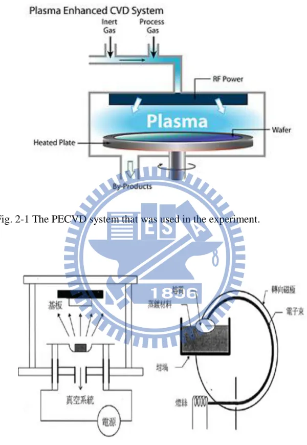
Fig. 2-1 The PECVD system that was used in the experiment. ... 56 Fig. 2-2 The E-gun system that was used in this experiment. ... 56 Fig. 2-3 (1) Si substrate RCA clean (2) Plasma fluorination treatment (3)
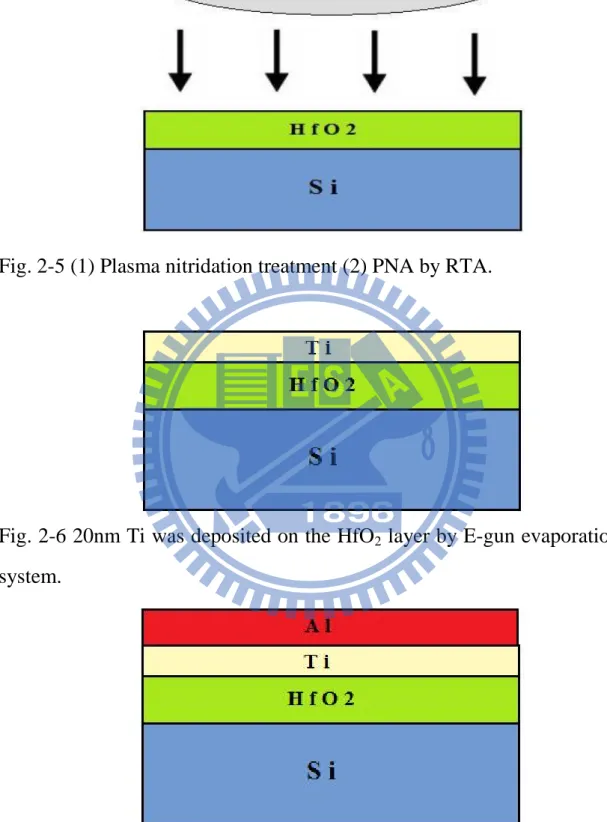
Annealing by RTA ... 57 Fig. 2-4 (1) 4nm HfO2 was deposited on the sub-Si by MOCVD (2)
PDA by RTA ... 57 Fig. 2-5 (1) Plasma nitridation treatment (2) PNA by RTA. ... 58 Fig. 2-6 20nm Ti was deposited on the HfO2 layer by E-gun
evaporation system. ... 58 Fig. 2-7 400nm Al was deposited on the Ti layer as top electrode by
E-gun evaporation system. ... 58 Fig. 2-8 Undefined Al was removed by wet etching. ... 59 Fig. 2-9 Undefined Ti was removed by wet etching (1%HF). ... 59 Fig. 2-10 Al was depodited on the back side of sub-Si as bottom
electrode by E-gun evaporation system . ... 59 Fig. 4-1 The capacitance-voltage (C-V) characteristics of HfO2 gate
X
Fig. 4-2 The J-V characteristics of p-type HfO2 capacitors treated in N2
plasma for different process time from 0V~-2V. ... 60 Fig. 4-3 The hysteresis of p-type HfO2 gate dielectrics without
treatment. ... 61 Fig. 4-4 The hysteresis of p-type HfO2 gate dielectrics treated in N2
plasma treatment 30 sec. ... 61 Fig. 4-5 The hysteresis of p-type HfO2 gate dielectrics treated in N2
plasma treatment 60 sec. ... 62 Fig. 4-6 The hysteresis of p-type HfO2 gate dielectrics treated in N2
plasma treatment 90 sec. ... 62 Fig. 4-7 The hysteresis of p-type HfO2 gate dielectrics treated in N2
plasma treatment 120 sec. ... 63 Fig. 4-8 The hysteresis of p-type HfO2 gate dielectrics treated in N2
plasma treatment 150 sec. ... 63 Fig. 4-9 The hysteresis of p-type HfO2 gate dielectrics treated in N2
plasma treatment 180 sec. ... 64 Fig. 4-10 The capacitance-voltage (C-V) characteristics of HfO2 gate
dielectrics treated in N2O phasma for different process time. ... 64
Fig. 4-11 The J-V characteristics of p-type HfO2 capacitors treated in
N2O plasma for different process time from 0V~-2V. ... 65
Fig. 4-12 The hysteresis of p-type HfO2 gate dielectrics without
treatment. ... 65 Fig. 4-13 The hysteresis of p-type HfO2 gate dielectrics treated in N2 O
plasma treatment 60 sec. ... 66 Fig. 4-14 The hysteresis of p-type HfO2 gate dielectrics treated with N2
XI
O plasma treatment 90 sec... 66 Fig. 4-15 The hysteresis of p-type HfO2 gate dielectrics treated in N2 O
plasma treatment 120 sec. ... 67 Fig. 4-16 The hysteresis of p-type HfO2 gate dielectrics treated in N2 O
plasma treatment 150 sec . ... 67 Fig. 4-17 The hysteresis of p-type HfO2 gate dielectrics treated in N2 O
plasma treatment 180 sec. ... 68 Fig. 4-18 The capacitance-voltage (C-V) characteristics of HfO2 gate
dielectrics treated in NH3 plasma for different process time. .... 68
Fig. 4-19 The J-V characteristics of p-type HfO2 capacitors treated in
NH3 plasma for different process time from 0V~-2V. ... 69
Fig. 4-20 The hysteresis of p-type HfO2 gate dielectrics without
treatment. ... 69 Fig. 4-21 The hysteresis of p-type HfO2 gate dielectrics treated in NH3
plasma treatment 60 sec. ... 70 Fig. 4-22 The hysteresis of p-type HfO2 gate dielectrics treated in NH3
plasma treatment 90 sec. ... 70 Fig. 4-23 The hysteresis of p-type HfO2 gate dielectrics treated in NH3
plasma treatment 120 sec. ... 71 Fig. 4-24 The hysteresis of p-type HfO2 gate dielectrics treated in NH3
plasma treatment 150 sec. ... 71 Fig. 4-25 The hysteresis of p-type HfO2 gate dielectrics treated in NH3
plasma treatment 180 sec. ... 72 Fig 4-26 The capacitance-voltage (C-V) characteristics of HfO2 gate
XII
and N2O plasma treatment at optimal condition. ... 72
Fig. 4-27 The J-V characteristics of p-type HfO2 capacitors treated in
N2 plasma treatment, NH3 plasma treatment, and N2O plasma
treatment at optimal condition from 0V~-2V. ... 73 Fig. 4-28 The capacitance-voltage (C-V) characteristics of HfO2 gate
dielectrics treated in CF4 plasma for different process time. ... 73
Fig. 4-29 The J-V characteristics of p-type HfO2 capacitors treated in
CF4 plasma treatment from 0V~-2V. ... 74
Fig. 4-30 The capacitance-voltage (C-V) characteristics of MIS capacitors treated in N2 plasma 120 sec and CF4 plasma for
different process time. ... 74 Fig. 4-31 The J-V characteristics of MIS capacitors treated in N2
plasma 120 sec and CF4 plasma for different process time from
0V~-2V. ... 75 Fig. 4-32 The hysteresis of MIS capacitors without treatment. ... 75 Fig. 4-33 The hysteresis of MIS capacitors treated in N2 plasma 120 sec
CF4 plasma 10 sec. ... 76
Fig. 4-34 The hysteresis of MIS capacitors treated in N2 plasma 120 sec
and CF4 plasma 20 sec. ... 76
Fig. 4-35 The hysteresis of MIS capacitors treated in N2 plasma 120 sec
and CF4 plasma 30 sec. ... 77
Fig. 4-36 The hysteresis of MIS capacitors treated in N2 plasma 120 sec
and CF4 plasma 40 sec. ... 77
Fig. 4-37 The capacitance-voltage (C-V) characteristics of MIS capacitors treated in NH3 plasma 120 sec and CF4 plasma for
XIII
different process time. ... 78
Fig. 4-38 The J-V characteristics of p-type MIS capacitors treated in N2 plasma 120 sec and CF4 plasma for different process time from 0V~-2V. ... 78
Fig. 4-39 The hysteresis of MIS capacitors without treatment. ... 79
Fig. 4-40 The hysteresis of MIS capacitors treated in NH3 plasma 120 sec and CF4 plasma 10 sec. ... 79
Fig. 4-41 The hysteresis of MIS capacitors treated in NH3 plasma 120 sec and CF4 plasma 20 sec. ... 80
Fig. 4-42 The hysteresis of MIS capacitors treated in NH3 plasma 120 sec and CF4 plasma 30 sec. ... 80
Fig. 4-43 The hysteresis of MIS capacitors treated in NH3 plasma 120 sec and CF4 plasma 40 sec. ... 81
Fig. 4-44 The capacitance-voltage (C-V) characteristics of MIS capacitors combined CF4 plasma treatment with N2 or NH3 plasma treatment at optimal condition. ... 81
Fig. 4-45 The J-V characteristics of MIS capacitors combined CF4 plasma treatment with N2 or NH3 plasma treatment at optimal condition from 0V~-2V. ... 82
Table ... 83
Table 1-1 Reliability difficult challenges. (ITRS : 2004 update) ... 83
Table 1-2 Basic characteristics of various high-k materials. ... 84
Table 2-1 Comparison of deposition techniques : PVD , ALCVD and MOCVD. ... 85
1
Chapter 1
Introduction
1.1 Background
The semiconductor industry has continued to prosper and also to foster the growth of multiple industries since the early 70s and has become a global industry in the 90s, as many semiconductor suppliers have established manufacturing or assembly facilities in multiple regions of the world. The Semiconductor Industry Association (SIA) in the United States extrapolates Moore’s law into the future to create a roadmap the predicts future developments in microelectronics based on silicon devices. The roadmap sets yearly targets for the performance of integrated circuits (IC) and defines the advances in semiconductor technology required to reach those goals. According th the ―Moore’s Law‖ which can see in Fig. 1-1, proposed by Gordon Moore in 1965, which states that ―the number of components per chip doubles every 18 months‖, pursuing better performance with lower cost in needed. The most significant trend for society is in decreasing cost-per-function, which has led to an enormous growth in the market for integrated circuits over the past forty years. Along with for dozens of year semiconductor industry vigorous development, the modern age consume the conformity electric circuit's intense demand regarding the high denseness as well as the low electricity.
Silicon-based microelectronic devices have revolutionized our world in the past three decades. Integrated circuits (IC), built up from many
2
silicon devices (such as transistors and diodes) on a single chip. It can produce the cheaper electronic memory, and faster and more powerful processors. The semiconductor industry has been driven by constantly increasing transistor counts and performance per integrated circuit (IC). The single biggest driver has been continually shrinking linewidths that allowed more and more transistors to fit into the same area and simultaneously improve performance. Historically linewidths have shrunk every three years, and recently linewidths have been shrinking every two years. In Metal-Oxide-silicon (MOS), the gate oxide thickness will affect the MOS processing speed. In order to increase the devices speed, therefore reduced thickness is necessary.
The silicon industry has been scaling silicon dioxide (SiO2)
aggressively for the past 15 years for low-power, high performance
Complementary Metal-Oxide-Semiconductor (CMOS) transistor
applications. Although metal-oxide-semiconductor(MOS) basic structure and the principle do not have the too big change until now, but the technology already advances mature 32 nanometer technology and gate oxide below 100 nanometer thickness from 70 age’s 10um gate width and several hundred meter gate dielectric layer thickness. In the scaling of MOS, reducing the thickness of gate stack with lower leakage current plays an important role. Although the leakage current of the devices with the same gate dielectric reduces with the scaling gate length and width, that leakage current density increases with the scaling of gate dielectrics. Therefore, the gate leakage current increases as the device size decreases and causes higher power consumption and degrade the reliability of the
3
devices.
For more than 30 years, SiO2 films have been the preferred material
for gate dielectric in MOS-based structures. A traditional Si-based MOS structure is obtained by growing a layer of silicon dioxide ( ) on top of silicon substrate and depositing a layer of metal or polycrystalline silicon. Silicon dioxide is a good candidate for gate because it has many advantages in IC technology. For example, it has good stability, high-quality Si/SiO2 interface, and outstanding isolation properties. SiO2
is an almost perfect insulator with a resistivity in excess of 1016Ωcm. The insulating films of SiO2 grown on silicon are smooth and coherent with
no holes in a thickness range down to single atomic layers. The interface with silicon is abrupt and there are very few electrically active defects at the interface.
MOSFET gate oxide scaling limits are examined with respect to time-dependent breakdown, defects, plasma process damage, mobility degradation, poly-gate depletion inversion later thickness m tunneling leakage, charge trapping, and gate delay. The formation of ultrathin high-quality gate dielectric has become one of most critical challenges for further downscaling of a device’s dimension. The challenges including two important reasons exist, first, the penetration and accumulation of boron into oxide critically degrades the intrinsic oxide reliability [1]. To solve this problem, it has been proposed to have a relatively high nitrogen concentration on the top poly/dielectric interface to block the boron diffusion. Second problem is excessive gate leakage current in ultrathin oxide. According to the SIA(Semiconductor Industry Association)
4
roadmap, CMOS with gate length below 70nm will need an oxide thickness of less than 1.5nm, which corresponds to two or three layers of silicon dioxide atoms which shows in Fig. 1-2 [2]. Direct tunneling current density at approximately 2nm thickness are about 10-2A/cm2. Further reduction in thickness will increase tunneling current exponentially.The resulting gate leakage current will increase the power dissipation and will deteriorate the device performance and circuit stability for VLSI circuits. The gate oxide must be reduced in turn, from 25 silicon atoms today to 5 atoms in 2012 to achieve the roadmap goal. In Fig. 1-3, it shows there must be a limit to this scaling down because the gate-oxide thickness will eventually reach zero [3]. For this reason, a global search for medium-and/or high-k materials for gate dielectric is necessary. The use of high-k materials makes the dielectric film physically thicker resulting in reduced gate leakage with respect to pure SiO2 film with same electrical thickness.
1.2 Scaling down of gate dielectric thickness
In terms of the first order current-voltage relation , the driving current of a MOSFET can be given as
(1.1)
(1.2)
Where Leff is the effective channel length, W is the channel width, VGS is
the applied gate to source, VT the threshold voltage, is the mobility
5
capacitance. Form (1.1) [4], we know that with smaller Leff (effective
channel length), reduced VT(threshold voltages), and increased Cg(gate
capacitance) as well as gate-to-source voltage, the device can achieve better current driving ability (increasing on-current). In addition, it can also have higher device density, which means a better performance and much more transistors on the chip. The gate oxide thickness required for good MOSFET control actually depends on the capacitance of the film. Capacitance is given by (1.2) [4], where is the dielectric constant, A is the area and is the electrical film thickness. So a bigger Cg and
shorter Leff will be needed to maintain device performance.
Over the past 30 years, SiO2 has been an perfect candidate for gate
dielectric , and has been scaled down from a thickness of 100nm to 1.2nm at 90nm process technology node today, in order to gain a large Cg and a
higher density. Unfortunately, the use of the traditional SiO2 gate
dielectric has become questionable for sub-0.25 m ULSI devices [5-8]. Increasing problems with dopant (boron) penetration through ultrathin SiO2 layers and direct tunneling for ultrathin (<2nm, which correspond to
two or three layers of silicon dioxide atom) oxide films dictate the search for and aggressive exploration of new materials to solve these problems for future gate dielectric.
There are the several kinds of conduction mechanisms of the leakage current passing through the oxide layer, which contain hot carrier injection, Fowler-Nordheim tunneling and direct tunneling which shows in Fig.1-4. Reducing the thickness of silicon dioxide is less than 2 nm, the dominant leakage mechanism is direct tunneling. The resulting of direct
6
tunneling current will increase the power dissipation and decrease the device performance and circuit stability. We can see the machine from (1.3)
(1.3)
`We can see form Fig.1-5 [9] to find that the gate oxide can be scaled down to 2nm before exceeding the limit of 1A/cm2 from the tolerant power consuming. Inversion channel charge loss caused by high gate leakage will degrade the device performance. The high gate leakage also increases standby power consumption.
1.3
The need to use High-k Dielectric
The recent downsizing of the Si device has significantly reduced the gate dielectric film thickness, so that the higher gate leakage on conventional SiO2 dielectrics has become serious. As use SiO2 to gate
dielectric is less than 2 nm, the leakage current become unacceptable. We can see (1.4) which be rewritten by (1.2).
(1.4)
Recently, high-k gate dielectrics as an alternative to conventional SiO2 gate oxides are widely investigated for their capability to reduce
gate leakage current for the same electrical capacitance [10]-[13]. From (1.4) the direct way to reduce the leakage current is to make the oxide thickness thicker, which can repress the direct tunneling current. We can see (1.5) which be rewritten by (1.4)
7
(1.5)
From (1.5), we use high-k material to be the gate dielectric which can maintain the same Equivalent oxide thickness (EOT) with thicker physical thickness, and is therefore expected drastically reduced the probability of direct tunneling current, and hence, reduces the amount of off-state leakage current density that we can see in Fig.1-6 [14]. The material with higher dielectric constant than 3.9 is called high-k material. In the last few years, high-k material has attracted a great deal of attention because of their promising for replacing SiO2 as gate dielectric in
MOSFETs. Nevertheless, the metal-gate electrode has also attracted attention as a solution to the polydepletion effect that appears under gate inversion conditions in poly-Si gates, as well as the incompatibility between some high-k materials and poly-Si [15].
1.4
Why choose HfO
2High-k materials have several advantages, such as being amorphous phase through the whole integration processing, high quality interface and good thermal stability. So, an ideal gate dielectric should meet the following requirements below :
Physical properties :
1. Gate material compatibility
Materials such as metal gate, and metals have been considered for better controllability and better performance. 2. Wide bandgap with conduction band offset > 1eV
8
wide enough bandgap. In contact with silicon and gate electrode, the bandgap is closely related to the barrier height for carrier transport. Low bandgap will lead to intolerably high gate leakage (leakage current ~exp(-△Ec)).
3. Suitable high-k value (12~60)
A suitable k value is indispensable. Those with not enough high k value could not satisfy (1.3) to lower the leakage by
increasing physical thickness. While those with too high k value, in general, would suffer from thermal stability issues and larger fringing field.
4. Film morphology(amorphous) and stable process compatibility In the VLSI process, the thermal budget is an important issue since high temperature changes dielectric phase. Once the gate dielectric material has transformed to polycrystalline from amorphous phase, the large grain boundaries would serve as leakage path, and induce large leakage current.
5. Thermodynamic stability in direct contact with silicon Preserve capacitance of gate stack after processing. Electrical Properties
1. Low interface state density (Dit< 5x10¹⁰/cm2-eV-1), and SiO2-like mobility, the interface would affect the carrier mobility in the channel, and from (1.2), mobility degradation is related to poor current drivability. In high-k, there are so many sources that would reduce mobility, such as fixed charge, remote phonon, interfacial dipoles, remote surface roughness, surface roughness and phase
9
separation crystallization. And most of them can be avoided by improving process technology.
2. No C-V dispersion 3. V FB and hysteresis < 20mV 4. J<10-3A/cm2@ VDD 5. T inv<1nm 6. Reliability issue
To serve as a new gate dielectric, we must also take into consideration electrical reliabilities, such as stress-induced leakage current (SILC), time dependent dielectric breakdown (TDDB), hot carrier aging, bias temperature instability and charge trapping issues [16].
There are many promising candidates for replacing SiO2, such as
HfO2, ZrO2, Al2O3, Y2O3, Ta2O3 and Ti2O3 etc. In Table 1-2 lists basic
characteristics of several high-k dielectrics. Unfortunately, many high-k materials such as SrTiO3, TiO2, Ta2O5 and BaSrTiO3 are thermally
unstable when directly contacted with silicon [17] and need an additional barrier layer which may add process complexity and impose thickness scaling limit. Also, materials with too low or too high dielectric constant may not be adequate choice for alternative gate dielectric application. Ultra high-k material such as STO or BST may cause fringing field induced barrier lowering effect [18]. Materials with relatively low dielectric constant such as Al2O3 and Y2O3 do not provide sufficient
advantages over SiO2 or Si3N4 [19]. Among the medium-k materials
10
recently. Especially, Hf forms the most stable oxide with the highest heat of formation (ΔHf = 27l Kcal/mol) among the elements in IVA group of the periodic table (i.e. Ti, Zr, Hf). Unlike other silicides, the silicide of Hf can be easily oxidized [20]. HfO2 possesses a dielectric constant of up to
25 [21], a large bandgap of 5.7 eV with sufficient band offset of larger than 1.5 eV [22], and well thermal stability in contact with silicon [23]. Fig.1-7 [24] shows HfO2 is the most suitable material about the struggle
between dielectric constant and bandgap. HfO2 is very resistive to
impurity diffusion and intermixing at the interface because of its high density (9.68 g/cm3) [25]. In addition, HfO2 is the first high-k material
showing compatibility with polysilicon gate process [26]. Therefore, among the high-k dielectrics being studied , HfO2 appears promising due
to its relatively high dielectric constant (~25) as compared to Si3N4 and
Al2O3 [27], its relatively high free energy of reaction with Si
(47.6Kcal/mole at 727℃) as compared to TiO2 and Ta2O5 [28], and its
relatively large bandgap (~5.8eV) [29]. These properties make HfO2to be
one of the most promising candidates for alternative gate dielectric application.
1.5 Challenges of High-k Material
The high-k material has attracted a great deal of attention because of their potential for replacing SiO2 as gate dielectric in MOSFETs. But
there are many problems to use high-k material practically. The issues for choosing a high-k material may include :
11
(2) Thermal stability
(3) Poly interface and poly gate electrode (4) Shift of threshold voltage
(5) Low dielectric constant interfacial layer between substrate and high-k material.
(6) Boron penetration prevention
(7) Compatibility with traditional CMOS process.
Table 1-1 shows the reliability challenges of high-k gate dielectrics, metal gate and copper/low-k interconnects. The main reliability issues include :
(1) Dielectric breakdown characteristic(hard and soft breakdown) (2) Influence of charge trapping and NBTI(Negative Bias
Temperature Instability) on threshold voltage stability. (3) Stability and unmber of fixed charges
All the issus mentioned above still need more effort to overcome .
Recently , HfO2-based insulator become promising candidates for the
gate dielectric , there still remain many challenges : (1) Extra interfacial layer growing lower the C value (2) The degradation of mobility [30]
(3) Threshold voltage instability and hysteresis issue [31] [32] (4) Charge-trapping issue [33]
(5) Thermal stability problem [35]
Therefore, high-k dielectrics although provide a low leakage current and satisfied capacitance, but the reliability issues can not be ignorable.
12
So, it needs some treatments to overcome these problems.
1.6 Charge trapping in HfO
2Even if HfO2 (and other high-k candidates) have several advantages,
such as being amorphous phase through the whole integration processing, high quality interface and good thermal stability , but there is still a number of fundamental issues, such as fixed charge, reduced channel mobility and trapped charge, which have to be understood and solved for successful high-k intergration into the Si CMOS technology [36][37].
Charge trapping in high-k gate stacks is known to be more severe compared to conventional SiO2-based gate dielectrics and due to cold
tunneling (i.e., from carriers assisted by the gate insulator field) can be characterized by followed by measurement of the shift in flatband or threshold voltage [37]. During device operation, some charge may be trapped as it passes through the gate stack causing device instabilities such as threshold voltage shifts and drive current degradation. Compared to SiO2, charge trapping in high-k is much more severe. We can see Fig
1-8 [38], electron transport in high-k gate dielectrics will instead be governed by trap-assisted mechanism, such as Frenkel-Poole (F-P) conduction or hopping conduction, due to the charge-trapping phenomenon. In order to explain higher current density traps in the band gap of the high-k dielectrics, charge trapping has to be assumed. In order to explain higher current density traps in the band gap of the high-k dielectrics, charge trapping has to be assumed. In the known trap-assisted tunneling (TAT) models and the F-P conduction mechanism, the current
13
density only linearly depends on the trap concentration [39]-[41]. The charging is believed to be mostly due to trapping on preexisting defects in the high-k layer and/or its interfaces.
.
1.7 Thesis Organization
Following chapters in the thesis are primarily organized as follow : In chapter 2, we describe the motivation for this thesis.
In chapter 3, we make a description of experimental details. Metal Organic Deposition system is used to deposit HfO2 on silicon surface.
In chapter 4, we discuss the electrical characteristics of HfO2
insulator by Metal Insulator Semiconductor (MIS) capacitors.
In chapter 5, we make the conclusions for this thesis and provide some suggestions for future work.
14
Chapter 2
Motivations
2.1 Forward
For more than 30 years, SiO2 films have been the preferred material
for gate dielectric in MOS-based structures, but the gate oxide scaling limits are examined with respect to time-dependent breakdown, defects, plasma process damage, mobility degradation, poly-gate depletion inversion later thickness m tunneling leakage, charge trapping, and gate delay. The recent downsizing of the Si device has significantly reduced the gate dielectric film thickness, so that the higher gate leakage on conventional SiO2 dielectrics has become serious. As use SiO2 to gate
dielectric is less than 2 nm, the leakage current become unacceptable. In the last few years, high-k material has attracted a great deal of attention because of their promising for replacing SiO2 as gate dielectric
in MOSFETs. Using hafnium oxide based materials are under intense investigation and optimization due to their high dielectric constant, wide band gap/barrier height and good thermal stability. While HfO2 (and
other high-k candidates) show the desired effect of significantly reducing gate tunneling (leakage) current. Therefore, to search for high dielectric constant (high-k) materials for near-future gate dielectrics in MOS ULSI devices is currently an enormous materials and technological challenge.
15
2.2 Plasma nitridaion
According to traditional view of improving SiO2 device performance,
we could find that nitridation is a common method to improve the interface [42]. Property with the result that there is often N
it or Dit in the
interface, imperfect bonding of interface usually makes the characteristic of the device deteriorate. For example, charge will be trapped by the defects of the interface, it produces flat band voltage shift and also reduces the carrier mobility. Another shortcoming is that these damgling bonds will easily bond with oxygen atoms in the following high temperature environment. The extra chemical reaction will let the interfacial oxide growth, and it will reduce the capacitance because of the lower dielectric constant. In addition, the quality of interfacial layer formed by oxidation is worse and there still will be the more problems of charge trapping.
In order to solve these problems, nitridation treatment could let the atom of nitrogen bond with these dangling bonds and fix it while entering the interface layer, and then improve the stability and reliability of interface. Therefore, nitridation treatment is a workable solution to improve interface quality. As note before m the problem about using high-k materials to replace SiO2 is that there are too many defects in the
interface to cause reliability degradation. Therefore, when we use high-k materials, it considers that nitridation treatment is a more suitable way to improve reliability and thermal stability of the device. There are several kind of treatment methods [43][44]. According to [45], we can understand that the effect of plasma nitridation is better than thermal nitridation
16
because high-k material are afraid of high temperature. As long as the temperature reaches certain degree, we can see phenomenon of crystallization. The crystallization of dielectric will raise leakage current substantially, because it offers the path of leakage current. On the other hand, the meaning of plasma nitridation is to activate the gas source first. The high activation energy of radical will provide better recovery which is better than thermal nitridation. For all these reasons, we adopt plasma nitridation to improve reliability in present experience.
2.3 Plasma fluorination
Threshold voltage instability and device degradation are still major concerns for MOSFETs using high-k gate dielectrics due to high interface and bulk density. Hydrogen (H) and deuterium (D) anneals have been found to help passivate these traps with significantly improved device performance [46]. But the bonding between high-k dielectric (or Si) and H is still not significantly stable to meet the requirement of reliability.
Recently, fluorinated gate dielectrics have been shown to improve the high-k (or Si)/Si interface [47][48]. The beneficial effects of fluorine for attaining more robust oxide have been attributed to its possible ability to improve the interfacial region by terminating the Si dangling bonds, strain relaxation due to breakup of highly strained Si-O-Si bonds by F [49][50], a higher bond strength of the Si-F bond (5.81eV) [51] compared to the Si-H bond (3.6eV) [52]. Thus, the pileup of F at the interface that replaces the Si-H bond by a stronger Si-F bond provides higher interfacial robustness. At the interface, where there are many Si damgling bonds, F
17
is effective in replacing weaker bonds. Therefore, for fluorination, fluorine can passivate the gap states of HfO2 completely. It has been
found that silicon incorporated HfO2 can enlarge the band gap, improve
the thermal stability performance, and suppress the crystallization.
2.4 Dual Plasma treatment
In this experiment, we expects to obtain the advantages that combined plasma fluorination with plasma nitridation. The method that combined plasma fluorination with plasma nitridation calls dual plasma treatment.
18
Chapter 3
Experiments of Al/Ti/HfO
2/Si MIS capacitor
3.1 Use MOCVD to prepare high-k thin film
There are several methods to prepare high-k film , such as chemical vapar deposition (i.e. ALCVD MOCVD PECVD etc.) [53]-[55] and physical vapor deposition (i.e. PLD , Sputtering , E-gun etc.)[56][57]. Table 2-1 is the comparison of deposition techniques which have been used. MOCVD has many advantages including high deposition rate, high crystallization without post annealing, large-area deposition, high
throughput, excellent uniformity, excellent step coverage on
three-dimensional complex geometries, flexibility for large-scale processing, and a simple experimental system compared to physical vapor deposition which requires high-vacuum equipments. Therefore, we used the MOCVD methods to prepare high-k film below.
MOCVD (Metal-Organic Chemical Vapor Deposition) is a widely used technology for depositing a variety of thin films, including metal oxide silicate films, for high-k gate dielectric applications. The basic steps in MOCVD deposition method are as follows :
1. MO precursor in company with N2 process gas and O2 process gas are
injected into the reactor.
2. The sources are mixed inside the reactor and transferred to the deposition process chamber.
19
3. At the deposition process chamber, high temperature results in the decomposition of sources and other gas-phase reactions, forming the film precursors that are useful for film growth and byproducts.
4. The film precursors transport to the growth surface. 5. The film precursors are absorbed on the growth surface. 6. The film precursors diffuse to the growth site.
7. At the surface, film atoms incorporate into the growing film through surface reaction.
8. The byproducts of the surface reactions desorb from the surface.
9. The byproducts transport to the main gas flow region away from the deposition area toward the reaction. Then the wafer exits.
3.2 Rapid thermal annealing system
METAL RTA-AG 610 was a single-wafer lamp-heated and computer controlled rapid thermal processing (RTP) system. Water and compressed dry air (CDA) cooling system were used to cool down the quartz chamber. High intensity visible radiation heating and cold-heating chamber walls allow fast wafer heating and cooling rate. The tungsten halogen lamps were distinguished into five groups, and the relative percentage of lamp intensity can be adjusted individually for each group to achieve uniform temperature distribution. Temperature was obtained from pyrometer and precise controlled by computer. Two gas lines were used in the system which can be switched between Ar and N2. Before
RTA process started, one minute N2 gas purge was performed to
20
unwanted particles induced during process. A fast heating rate of 100℃/s was chosen in this work. When anneal was complete, chamber
temperature was quickly cooled down from 900℃ to 500℃ by N2 purge
30 seconds. Then, the chamber was slowly cooled down to 280 without N2 purge to avoid creaking of films. After five minutes later, wafers can
be taken out from the chamber. Films’ creak can be avoided by two-steps-cooling method.
3.3 Plasma treatment system
In this experiment, we use plasma pre-treatment (before HfO2 film
deposition) Si surface after RCA clean to improve the High-k/Si interface quality. When the PDA (Post-Deposition-Annealing) was finished, some samples also were subjected to an additional plasma treatment in order to improve the electrical properties of gate dielectric. There were various source gas (N2, N2O, NH3, CF4) and process time (10~120 seconds) as the
experiment conditions. Fig 2-1 illustrates that PECVD (Plasma-enhanced chemical vapor deposition) is a process used to deposit thin films from a gas state (vapor) to a solid state on a substrate. Chemical reactions are involved in the process, which occur after creation of plasma of the reacting gases. The plasma is generally created by RF (AC) frequency or DC discharge between two electrodes, the space between which is filled with the reacting gases.
The PECVD system in this experiment which is a Samco model PD-220N. This is a CVD system designed for low temperature (typically ~ 200-400℃) depositon of silicon based materials. It’s also provides the
21
capacity to process five 3‖ wafers , three 4‖ wafers , or one 8‖ wafer per cycle.
3.4 E-gun system
After plasma treatment and PNA, we deposited Ti and Al as electrical by E-gun. And finished all manufacturing process, we used E-gun deposited Al as back electrical too. Figure 2-2 shows E-gun work theorem, the system is always in vacuity, and the materials which we wanted to deposited was in the boat. We melt down the materials by heating, and using the electron-beam to bombard the materials to proceed evaporation. The chamber pressure was 10-6 mTorr when we deposited. After the deposited Ti and Al we could proceed lithography and etching.
3.5 MIS capacitors fabrication process
For the purposes of this research, MOS capacitors were fabricated. The silicon wafer used in this experiment were four inch (100) orientated p-type wafer. It was on side polished and its resistivity 5~10 ohm-cm.
3.5.1 The experiment of plasma fluorination treatment
After standard initial RCA clean, wafers were put into chamber of the PECVD and plasma fluorination treats the Si surface. The plasma fluorination treatment conditions were in pure CF4 gas for 10 sec, 20 sec,
30 sec, and 40 sec respectively and the flow rate were 100 sccm and bias 20W in the 300℃ environment.
22
After the plasma treatment were finished, the wafers were put into chamber and grew HfO2 layer with MOCVD. After the thin films were
deposited, most samples were annealed in a N2 ambient for 30 sec at
600℃ after deposition (PDA , Post-Deposition Anneal) by rapid thermal annealing (RTA). Pure titanic was deposited on the HfO2 layer by e-gun
evaporation system and aluminum films were evaporated on the top side of wafers. Mask defined the top electrode. Then, we used wet etching to etch undefined Al and Ti films. After patterning, backside native oxide was stripped with diluted HF solution, and Al was deposited as bottom electrode. The detailed fabrication process flow was listed as follows 1. As shown in Fig 2-3
(1) Si substrate RCA clean
(2) Plasma fluorination treatment (3) Annealing by RTA
2. As shown in Fig 2-4
(1) 4nm HfO2 was deposited on the sub-Si by MOCVD.
(2) PDA by RTA 3. As shown in Fig 2-6
20nm Ti was deposited on the HfO2 layer by E-gun evaporation
system.
4. As shown in Fig 2-7
400nm Al was deposited on the Ti layer as top electrode by E-gun evaporation system.
5. As shown in Fig 2-8
23
6. As shown in Fig 2-9
Undefined Ti was removed by wet etching (1%HF). 7. As shown in Fig 2-10
Al was depodited on the back side of sub-Si as bottom electrode by E-gun evaporation system.
3.5.2 The experiment of plasma nitridation treatment
After standard initial RCA clean, wafers were put into chamber and grew HfO2 layer with MOCVD system. After the thin film were deposited,
some samples were annealed by rapid thermal annealing (RTA) and then we used the PECVD to plasma nitridation treat the high-k surface. The plasma treatment conditions were in pure N2, NH3, and N2O gas for 120
sec respectively and the flow rate were 100 sccm and bias 20W in the 300℃ environment. Pure titanic was deposited on the HfO2 layer by
e-gun evaporation system and aluminum films were evaporated on the top side of wafers. Mask defined the top electrode. Then, we used wet etching to etch undefined Al and Ti films. After patterning, backside native oxide was stripped with diluted HF solution, and Al was deposited as bottom electrode. The detailed fabrication process flow was listed as follows.
1. As shown in Fig 2-4
(1) Si substrate RCA clean
(2) 4nm HfO2 was deposited on the sub-Si by MOCVD.
(3) PDA by RTA 2. As shown in Fig 2-5
24
(1) Plasma nitridation treatment (2) PNA by RTA
3. As shown in Fig 2-6
20nm Ti was deposited on the HfO2 layer by E-gun evaporation
system.
4. As shown in Fig 2-7
400nm Al was deposited on the Ti layer as top electrode by E-gun evaporation system.
5. As shown in Fig 2-8
Undefined Al was removed by wet etching. 6. As shown in Fig 2-9
Undefined Ti was removed by wet etching (1%HF). 7. As shown in Fig 2-10
Al was deposited on the back side of sub-Si as bottom electrode by E-gun evaporation system..
3.5.3 Dual plasma treatment for MIS capacitors
After standard initial RCA clean, wafers were put into chamber of the
PECVD and plasma fluorination treats the Si surface. The plasma fluorination treatment conditions were in pure CF4 gas for 10 sec, 20 sec,
30 sec, and 40 sec respectively and the flow rate were 100 sccm and bias 20W in the 300℃ environment. After the plasma treatment were finished, the wafers were put into chamber and grew HfO2 layer with MOCVD.
25
ambient for 30 sec at 600℃ after deposition (PDA, Post-Deposition Anneal) by rapid thermal annealing (RTA). Then, we used the PECVD again to plasma nitridation treat the high-k surface. The plasma treatment conditions were in pure N2, NH3, and N2O gas for 120 sec, and
respectively and the flow rate were 100 sccm and bias 20W in the 300℃ environment. Pure titanic was deposited on the HfO2 layer by e-gun
evaporation system and aluminum films were evaporated on the top side of wafers. Mask defined the top electrode. Then, we used wet etching to etch undefined Al and Ti films. After patterning, backside native oxide was stripped with diluted HF solution, and Al was deposited as bottom electrode. The detailed fabrication process flow was listed as follows. 1. As shown in Fig 2-3
(1) Si substrate RCA clean
(2) Plasma fluorination treatment (3) Annealing by RTA
2. As shown in Fig 2-4
(1) 4nm HfO2 was deposited on the sub-Si by MOCVD.
(2) PDA by RTA 3. As shown in Fig 2-5
(1) Plasma nitridation treatment (2) PNA by RTA
4. As shown in Fig 2-6
20nm Ti was deposited on the HfO2 layer by E-gun evaporation
system.
26
400nm Al was deposited on the Ti layer as top electrode by E-gun evaporation system.
6. As shown in Fig 2-8
Undefined Al was removed by wet etching. 7. As shown in Fig 2-9
Undefined Ti was removed by wet etching (1%HF). 8. As shown in Fig 2-10
Al was depodited on the back side of sub-Si as bottom electrode by E-gun evaporation system.
3.6 The MIS Capacitors measurement
After the Al/Ti/ HfO2 /Si MIS capacitors were prepared, we used semiconductor parameter analyzer (HP4156C) and C-V measurement (HP4284) to analysis electric characteristics (i.e. I-V, C-V, EOT, leakage current density etc.).
27
Chapter 4
Electrical characteristics of Al/Ti/HfO2/Si MIS capacitors
In order to measure the C-V characteristics of our MIS capacitors, we used HP 4284A precision LCR meter in our experiments. We swept the gate bias from inversion region to accumulation region to obtain the curve at the frequency of 50 kHz from -2V to 1V. And the leakage current of our MIS capacitors were analyzed from the current-voltage (I-V) characteristics measured by an HP4156A semiconductor parameter analyzer. There are four kinds of plasma treatment with different souce gas (i.e. N2 , N2O , NH3) for different process time (i.e. 0 sec , 30sec ,
60sec , 90sec , 120sec , 150sec , 180sec ) and CF4 plasma treatment for
different process time (i.e. 0sec , 10sec , 20sec, 30sec , 40sec). Finally, we combine the two plasma process to obtain the optimal condition. Hence, the relationship of difference process time with CF4 in one kinds of
plasma treatment will be discussed.
The hysteresis will also be discussed in this experiment. The name of Hysteresis was borrowed from electromagnetic. It is means that when a ferromagnetic material is magnetized in one direction, it will not relax back to zero magnetization when the applied magnetizing field is removed. It must be driven back to zero by the additional opposite direction magnetic field. If an alternating magnetic field is applied to the material, its magnetization will trace out a loop called a hysteresis loop [58]. The hysteresis phenomenon is similar to the C-V curve in the MIS capacitor device. When we apply a voltage in reverse, it will not fit the
28
original C-V curve measured previously. It is due to the interface traps which can trap charges to have impact on the flat band voltage and C-V curve. The C-V characteristics for hysteresis extraction were measured by sweeping the voltage from accumulation to inversion (-2V→1V) and then sweeping back (1V→-2V) at a frequency of 50kHz.
4.1 Electrical characteristics for HfO
2with nitridation
plasma treatment
There are three kinds of plasma treatment with different source gas (i.e. N2, N2O, NH3) and they were treated for different process time (i.e.
30 sec, 60sec, 90sec, 120sec, 150sec and 180sec).
4.1.1 Electrical characteristics for HfO
2with N
2plasma
treatment for different process time
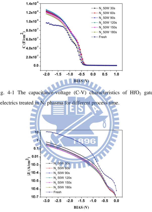
Fig. 4-1 reveals the capacitance-voltage (C-V) characteristics of HfO2 gate dielectrics treated in N2 plasma and DC bias 50W for different
process time. The capacitor treated in N2 for 120 sec shows the maximum
capacitance density among these samples with different process time. In addition, other samples which treated in N2 plasma all present the larger
values than the capacitors without whole plasma nitridation process. This phenomenon indicates that the N2 plasma treatment was workable to
improve the capacitance. The factor of improvement might be from that the PDA process and the nitrogen incorporation in the HfO2 dielectrics,
29
which could enhance the electronic polarization as well as the ionic polarization, so the dielectric constant of the HfO2 thin films increases
just as Hf-silicate thin film and SiO2 thin film. Besides, the capacitance
density of the samples treated in N2 plasma for 150 sec and 180 sec are
degraded. The reason could be the damage caused by the N2 plasma.
The J-V characteristics of the HfO2 capacitors treated by N2
plasma and DC bias 50W with different process time from 0V to -2V are described in Fig. 4-2. It can be observed that the samples which treated in N2 plasma all present the smaller leakage current density than the leakage
current density without whole plasma nitridation process. The gate leakage current density treated in N2 for 120 sec shows the minimum
current density among these conditions. The lower leakage shows that the weak structure of interface must be fixed by the plasma nitridaiton. In Fig. 4-1 and Fig. 4-2, it appears that the samples treated in N2 plasma for 120
sec display the most excellent value. While the nitridation process time is longer than 120 sec, the plasma damage from the plasma nitridation could cause the increase of the gate leakage density.
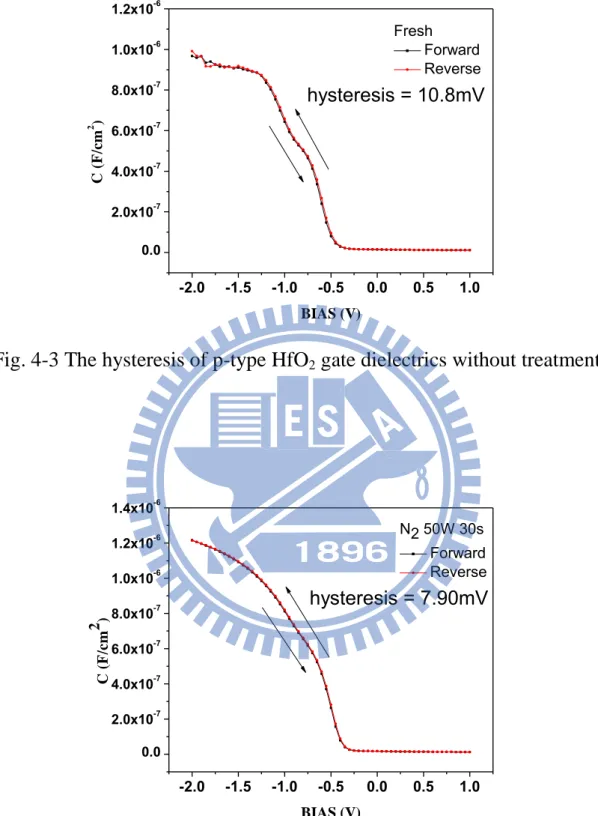
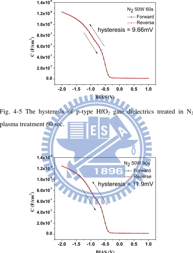
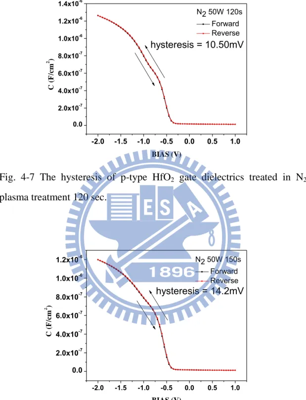
The hysteresis of C-V characteristics are shown in Figs. 4-3, 4-4, 4-5, 4-6, 4-7, 4-8, and 4-9 for the samples without treatment, and with 30, 60, 90, 120, 150, and 180 sec N2 plasma treatment , respectively. The
hysteresis phenomenon of the C-V curves can be observed for all samples, which is caused by the existence of negative charges trapped in the dielectric defect states when the capacitors are stressed. The hysteresis characteristic could be improved by various plasma nitridation process. In Figs.4-3, 4-4, and 4-5, the hysteresis was a slightly reduced after N2
30
plasma treatment because the nitrogen incorporation in the HfO2
dielectrics and reduced the interface trap state, thus improving hysteresis. In Fig.4-6, 4-7, 4-8, and 4-9, the hysteresis was a slightly enhanced more than other samples with N2 plasma treatment due to plasma damage.
However, these hysteresis voltage are very close to each other and can be acceptable.
4.1.2 Electrical characteristics for HfO
2with N
2O plasma
treatment for different process time
Fig4-10 reveals the capacitance-voltage (C-V) characteristics of HfO2
gate dielectrics treats in N2O plasma and DC bias 40W for different
process time. The capacitor treated in N2O 10 sec shows the maximum
capacitance among these samples with different process time, just like the group of N2 plasma treatment. In addition, other samples which treated in
N2O plasma all present the larger values than the capacitors without
whole plasma nitridation process. This phenomenon indicates that the N2O plasma treatment was workable to improve the capacitance. The
factor of improvement might be from that the PDA process and the nitrogen incorporation in the HfO2 dielectrics, which could enhance the
electronic polarization as well as the ionic polarization, so the dielectric constant of the HfO2 thin films increases just as Hf-silicate thin film and
SiO2 thin film. Besides, the capacitance density of the samples treated in
N2O plasma for 150 sec and 180 sec are degraded. The reason could be
31
The J-V characteristics of the HfO2 capacitors treated by N2O
plasma and DC bias 40W with different process time from 0V to -2V are described in Fig. 4-11. It can be observed that the samples which treated in N2 plasma all present the smaller leakage current density than the
leakage current density without whole plasma nitridation process. The gate leakage current density treated in N2O for 120 sec shows the
minimum current density among these conditions. The lower leakage shows that the weak structure of interface must be fixed by the plasma nitridaiton. In Fig. 4-10 and Fig. 4-11, it appears that the samples treated in N2O plasma for 120 sec display the most excellent value. While the
nitridation process time is longer than 120 sec, the plasma damage from the plasma nitridation could cause the increase of the gate leakage density.
The hysteresis of C-V characteristics are shown in Figs. 4-12, 4-13, 4-14, 4-15, 4-16, and 4-17 for the samples without treatment, and with 60, 90, 120, 150, and 180 sec N2 plasma treatment respectively. The
hysteresis phenomenon of the C-V curves can be observed for all samples, which is caused by the existence of negative charges trapped in the dielectric defect states when the capacitors are stressed. The hysteresis characteristic could be improved by various plasma nitridation process. It can be observed that the samples which treated in N2O plasma all
present the smaller values than the leakage current density without whole plasma nitridation process. The hysteresis was a slightly reduced after N2
plasma treatment because the nitrogen incorporation in the HfO2
32
However, these hysteresis voltage are very close to each other and can be acceptable.
4.1.3 Electrical characteristics for HfO
2with NH
3plasma
treatment for different process time
Fig. 4-18 shows the capacitance-voltage (C-V) characteristics of HfO2 gate dielectrics treated in NH3 plasma and DC bias 40W for
different process time. The capacitor treated in NH3 for 120sec shows the
maximum capacitance density among these samples with different process times. In addition, other samples which treated in NH3 plasma all
present the larger values than the capacitors without whole plasma nitridation process. This phenomenon indicates that the NH3 plasma
treatment was workable to improve the capacitance. The factor of improvement might be from that the PDA process and the nitrogen incorporation in the HfO2 dielectrics, which could enhance the electronic
polarization as well as the ionic polarization, so the dielectric constant of the HfO2 thin films increases just as Hf-silicate thin film and SiO2 thin
film. Besides, the capacitance density of the samples treated in NH3
plasma for 150 sec and 180 sec are degraded. The reason could be the damage caused by the NH3 plasma.
The J-V characteristics of the HfO2 capacitors treated by NH3
plasma and DC bias 40W with different process time from 0V to -2V are described in Fig. 4-19. It can be observed that the samples which treated in N2 plasma all present the smaller leakage current density than the
33
gate leakage current density treated in NH3 for 120 sec shows the
minimum current density among these conditions. The lower leakage shows that the weak structure of interface must be fixed by the plasma nitridaiton. In Fig. 4-18 and Fig. 4-19, it appears that the samples treated in NH3 plasma for 120 sec display the most excellent value. While the
nitridation process time is longer than 120 sec, the plasma damage from the plasma nitridation could cause the increase of the gate leakage density.
The hysteresis of C-V characteristics are shown in Figs. 4-20, 4-21, 4-22, 4-23, 4-24, and 4-25 for the samples without treatment, and with 60, 90, 120, 150, and 180 sec NH3 plasma treatment respectively. The
hysteresis phenomenon of the C-V curves can be observed for all samples, which is caused by the existence of negative charges trapped in the dielectric defect states when the capacitors are stressed. The hysteresis characteristic could be improved by various plasma nitridation process.
In Figs.4-20, 4-21, and 4-22, the hysteresis of NH3 plasma treatment
for 60 sec and 90 sec were both larger than the sample of no plasma treatment. The reason possibly was the plasma process times not enough. In Figs.4-23, 4-24, and 4-25, the hysteresis was a slightly reduced after NH3 plasma treatment because the nitrogen incorporation in the HfO2
dielectrics and reduced the interface trap state, thus improving hysteresis. However, these hysteresis voltage are very close to each other and can be acceptable.
34
4.1.4 Short summary
Fig. 4-26 shows the capacitance-voltage (C-V) characteristics of HfO2 gate dielectrics treated in N2, N2O, and NH3 plasma at optimal
condition. It is indicated that the capacitance treated in N2 plasma for 120
sec shows the most excellent value.
The J-V characteristics of the HfO2 capacitors treated in N2, N2O,
and NH3 plasma at optimal condition in Fig. 4-27. It is indicated that the
capacitance treated in N2O plasma for 120 sec shows the most excellent
value.
By the compare of the samples which has the best capacitance in their own gas, we can realize the most suitable treatment condition which both has the best capacitance and lower leakage current. Hence, we significantly find a relative optimal condition among above discussion. It is proved that without thick oxidation layer, it can also reach the smallest leakage current when there is suitable time treatment.
4.2 Electrical characteristics for HfO
2with fluorination
plasma treatment
Fig. 4-28 shows the capacitance-voltage (C-V) characteristics of Si surface (before HfO2 film deposited) treated in CF4 plasma and DC bias
20W for different process time. It indicated that the capacitance increases along with the time of plasma treatment. The capacitor treated in CF4 for
60 sec shows the maximum capacitance density among these samples with different process time. In addition, other samples which treated in
35
CF4 plasma all present the larger values than the capacitors without whole
plasma fluorination process. This phenomenon indicates that the CF4
plasma treatment was workable to improve the capacitance.
The factor of improvement might be from that the PDA process and the fluorine incorporation at the interface.
The J-V characteristics of the HfO2 capacitors treated by CF4 plasma
and DC bias 20W with different process time from 0V to -2V are described in Fig. 4-29. Compared with the control sample, the gate leakage current was decreased for the samples with CF4 plasma treated in
10 sec and 20 sec. The gate leakage current density treated in CF4 for 10
sec shows the minimum current density among these conditions. The lower leakage shows that the weak structure of interface must be fixed by the plasma fluorination. However, there is a non-ideal result that the gate leakage current increased for the sample with CF4 plasma treated in 30
sec and 40 sec. The reason for this phenomenon may be plasma damage and resulting in higher leakage current.
4.3 Electrical characteristics for HfO
2with dual plasma
treatment for different process time
There are three kinds of plasma treatment with different source gas (i.e. CF4, N2, NH3) and they were treated for different process time (i.e.
10 sec, 20sec, 30sec, 40sec, and 120sec).
![Fig. 1-3 With the marching of technology nodes, gate dielectric has to be shrunk and five silicon atoms thick of gate dielectric is predicted for 2012[3]](https://thumb-ap.123doks.com/thumbv2/9libinfo/8751875.206100/68.892.229.709.108.428/marching-technology-nodes-dielectric-shrunk-silicon-dielectric-predicted.webp)
![Fig. 1-7 Static dielectric constant vs. band gap for candidate gate oxides, after Robertson [8]](https://thumb-ap.123doks.com/thumbv2/9libinfo/8751875.206100/70.892.143.737.165.846/fig-static-dielectric-constant-candidate-oxides-after-robertson.webp)