A Miniature 15-50-GHz Medium Power Amplifier
Mei-Chen Chuang, Pei-Si Wu, Ming-Fong Lei, Huei Wang, Yu-Chi Wang*, and Chan Shin Wu*
Dept. of Electrical Engineering and Graduate Institute of Communication Engineering,
National Taiwan University, Taipei, Taiwan, 106, ROC
*WIN Semiconductors Corp., Hwaya Technology Park, Taiwan 333, ROC
Abstract — A miniature power amplifier, which combines
two conventional distributed amplifiers and a single transistor amplifier is designed to achieve wide bandwidth, high gain and moderate output power from 15 to 50 GHz. This circuit was fabricated using 0.15-μm GaAs based pHEMT MMIC technology. The measured small signal gain is 21±1.5dB from 15 to 50 GHz, and the output saturated power is 18-22 dBm from 18 to 50 GHz with a miniature size of 1.5 x 1 mm2.
Index Terms — Broadband, Power amplifier, Monolithic
Integrated circuit (MMIC).
I. INTRODUCTION
Broad-band power amplifier is very useful since it can cover many bands. Thus, it can be used in many applications without expensing time to fabricate another circuit which designed to cover the other band. Wide-band solid-state power amplifiers are difficult to design, because it is not easy to realize the power and bandwidth at the same time. For frequency higher than 50 GHz, the cascaded configuration demonstrated moderate bandwidth [1]-[2]. However, to design a lower frequency broadband power amplifier using this architecture will consume large chip area, since multistage matching networks are needed to achieve the bandwidth requirement. Balance amplifiers can achieve broadband gain and good VSWR at the expense of doubling the dc power and chip area [3]. Distributed amplifier (DA) is a well known broadband amplifier configuration, with the advantages of uniform gain, good noise figure and low VSWR performance over a wide frequency range [4]-[7]. One of the major drawbacks of this architecture is the dc power consumption due to the terminating resistors, which the dc current will flow through. There are some more improved architectures to design broad-band power amplifier [8]-[10]. In [8], one conventional distributed amplifier as the input stage and cascaded two single ended amplifiers as the second stage and output stage was reported. It can provide broadband gain response with ± 5dB ripple, but the output power is only 16 dBm in average. Conventional
distributed amplifier as the input stage cascaded with a CSSDA as the output stage has also been demonstrated [9]. The CSSDA output stage requires a termination resistor in its dc path, thus increasing the power consumption of the circuit significantly. Another amplifier cascading two CDA stages, have also been reported [10], but the dc power consumption is relatively large due to the output DA circuit architecture.
In this paper, a broadband medium power amplifier using 0.15-μm GaAs based pHEMT MMIC technology is presented. Two cascaded DA stages are used to provide wideband gain, with a final single-ended power stage to provide higher output power due toe the power matching network. Only two devices are used in each distributed amplifier stage in order to reduce the dc power consumption. This medium power amplifier demonstrates a measured gain of 21 ± 1.5 dB from 15 to 50 GHz, output 1-dB compression power (OP1dB) of 15.1 to 19.1 dBm
from 20 to 47 GHz, and saturated output power (Psat) of 18-22 dBm from 18 to 50 GHz with a compact chip size of 1.5 x 1 mm2. The amplifier can cover the frequency
from 15 to 50 GHz. Thus, it can be used in local multipoint distribution service (LMDS) at 28 GHz, and point-to-point microwave radio as well as automotive 24 GHz, instrumentation, and VSAT satellite ground stations. Broadband operation results in flexibility, economics of scale and improved inventory costs [11].
II. CIRCUIT DESIGN
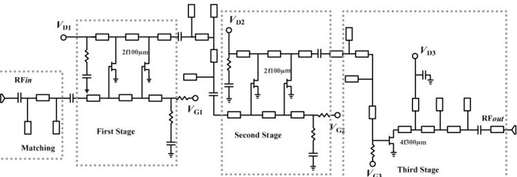
Figure 1 shows the circuit schematic diagram of the broadband medium power amplifier. The circuit cascades two distributed amplifier stages and a single transistor power stage. The first and second stages using distributed structure are designed for wide bandwidth and high gain. The third stage is designed for output power. By using this architecture, high gain and flat output power can be achieved over a wide bandwidth. The first stage and
Fig. 1. Circuit schematic diagram of the 15-50 GHz medium power amplifier
the second stage utilize two distributed cells to provide broadband gain. The devices in these two cells are all 2-finger with total gate width of 100-μm HEMT devices. Since the power dissipation is an important issue for distributed amplifier, there are only two transistors in each stage. Series R-C bypass circuits are used as terminations in the gate and drain bias, and therefore the current will not flow through the resistors and consume dc power on the termination resistors. The third stage is a single transistor amplifier designed for large output power and wide bandwidth. The device size of the third stage is 4-finger with total gate width of 300-μm.
Fig. 2. Chip photo of the 15-50 GHz amplifier with chip size of 1.5 x 1 mm2
This circuit is fabricated using the 0.15-μm GaAs pHEMT process provided by WIN Semiconductors. The unit current gain frequency (fT) of the device is about 85
GHz, and the maximum oscillation frequency (fmax) is over
120 GHz. The typical breakdown voltage is 10 V and the
peak of trans-conductance is 495 mS/mm. Other passive components such as thin-film resistors, MIM
(a)
(b)
Fig. 3. Simulated and measured (a) small signal gain, and (b) input and output return loss, versus frequency for 15-50 PA.
capacitors, spiral inductors, and air-bridges are available. The 6” wafer is thinned down to 4-mil for the gold plating of the backside, and slot via holes are used for dc grounding.
The complete circuit is simulated using ADS circuit simulator [12]. All the passive components, such as junctions, capacitances, and transmission lines are simulated using a full-wave EM simulator provided by Microwave Office [13]. The chip photo is shown in Fig. 2, with a chip size of 1.5 mm x 1 mm.
III. MEASUREMENT
The performance of the chip was measured via on-wafer probing. An HP8510C measurement system is used to measure the small signal frequency response to from 45 MHz to 50 GHz.
Figure 3(a) shows the measured and simulated small signal gain, while Fig. 3(b) presents the input and output return losses of this power amplifier from 0.045 to 50 GHz. The first stage is biased at Vgs = -0.25 V, Vds = 3 V with Id = 47 mA, while the second stage is biased at Vgs = -0.25 V, Vds = 4 V and Id with 58 mA, and the third stage at Vgs = -0.25 V, Vds = 3 V with Id = 69 mA. The small signal gain is 21 dB with less than 1.5 dB ripple over 15 to 50 GHz. The total dc power consumption is 649 mW. Because the third stage of this amplifier is a band pass design, it has no gain at lower frequency (below
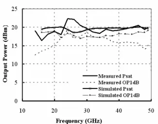
15 GHz). Power performance was measured using an HP83650B signal generator and a power amplifier for large RF power input up to 50 GHz. Figure 4 illustrates the measurement and simulation of saturated power vs. the frequency and the measured and simulated output P1dB
(OP1dB) versus frequency. The measured OP1dB is
between 15.1 to 19.1 dBm from 20 to 47 GHz. The measured saturated power is between 18 to 22 dBm from 18 to 50 GHz. Table I compares the recently reported broad-band amplifiers, including reported literature and commercial products. Compared with the reported broadband power amplifiers, this chip provides flat gain, 20 dBm average power over a wide-bandwidth in a compact small chip size.
IV.CONCLUSION
A 15-50 GHz high gain GaAs MMIC medium power amplifier has been designed, fabricated, and measured. It provides flat gain and sufficient power over the operating frequency. The small signal gain is 21 dB with 1.5 dB ripple over 15 to 50 GHz. The saturated power is 18 to 22 dBm output power over 18 to 50 GHz and the OP1dB is
15.1 to 19.1 dBm from 20 to 47 GHz. The wide bandwidth and power make this amplifier suitable in many microwave system applications, such as measurement instruments, and transceiver gain block.
Frequency (GHz)
Architecture Process PSAT (dBm) Gain
(dB)
Size (mm2)
PDC (mW)
[6] DC-54 (device cascode) CDA 0.15μm GaAs HEMT 23 15 ± 0.5 6.07 1100
[8] 18-71 stage amplifier CDA+2 single 0.15μm GaAs pHEMT 16 (19~57 GHz) 20 ± 5 2.5 306
[9] 0.1-40 CDA+2CSSDA 0.15μm GaAs pHEMT 15 22 ± 2 3 480
[10] 4-37 2 CDA 0.15μm GaAs pHEMT 20.6-23.3 15.3 ± 1 3 1642
[11] 1-40 CDA (device cascode) 0.15μm GaAs pHEMT 20-25 13.5 ± 1.5 2.47 1400
[14] 0.1-65 CDA (device cascode) 0.15μm GaAs MHEMT N/A 14 ± 2.5 1.59 105
[15] 18-40 stage amplifier CDA + single HEMT GaAs 14 12.5 1.53 240
[16] 17-40 DA+3 single stage amplifier GaAs HEMT 21 21 1.51 1170
This work 15-50 2 CDA + single stage amplifier 0.15μm GaAs pHEMT 18-22 (18-50GHz) 21 ± 1.5 1.5 649
Fig. 4. Simulated and measured OP1dB and PSAT vs. frequency
for the 15-50 GHz medium power amplifier.
ACKNOWLEDGEMENT
This work is supported in part by the National Council of Taiwan, R.O.C. under Projects NSC 93-2219-E-002-024, NSC 93-2213-E-002-033 and NSC 93-2752-E-002-002-PAE. The chip is fabricated on WIN semiconductor. The authors wish to acknowledge the software support of Chip Implementation Center of Taiwan.
REFERENCES
[1] L. Samoska, Y. C. Leong, “65-145 GHz InP MMIC HEMT medium power amplifier,” 2001 IEEE MTT-S Int.
Microwave Symp. Dig., pp.1805-1808, May 2001.
[2] Y. C. Leong, S. Weinreb, “Full W-band MMIC medium power amplifier,” 2000 IEEE MTT-S Int. Microwave Symp. Dig., vol 2, pp. 951-954, June 2000. [3] Vaz, J.C., and Freire, J.C.,” Millimeter-wave monolithic power amplifier for mobile broad-band systems” IEEE Trans. Microwave
Theory Tech., vol. 49, 2001, June, pp.1211-12152196
[4] H.B Demuth, “An investigation of the iterative synthesis of distributed amplifiers,” Stanford Univ. Elect. Lab.,
Technique Report no. 77; August 1954
[5] Y. Baeyens et al., “InP D-HBT ICs for 40-Gb/s and higher bit rate lightwave transceivers.” IEEE J. Solid State
Circuits, vol. 37, pp. 1152-1159, Sept. 2002
[6] H.Shigematsu, N.Yoshida, M.Sato, T.Hirose, and Y. Watanabe, “45-GHz distributed amplifier with linear 6 Vp-p outVp-put for a 40-Gb/s LiNbO3 modulator driver circuit,” 2001 MTT-S Int Microwave Symp. Dig., vol. 1, pp.137-140, June 2001.
[7] C. Meliani, G. Post, G. Rondeau, J. Decobert, W. Mouzannar, E. Dutisseuil and R. Lefevrem “DC-92 GHz ultra-broadband gain InP HEMT amplifier with 410 GHz gain-bandwidth product,” Electronic Lett., vol.38, pp.1175-1176, Sept. 2002
[8] P. S. Wu, T. W. Huang, and H. Wang, “An 18-71 GHz multi-band and high gain GaAs MMIC medium power amplifier for millimeter-wave applications,” IEEE MTT-S
Int. Microwave Symp. Dig., June 2003, pp. 863-866
[9] K. L. Deng, T.W. Huang, and H.Wang, “Design and analysis of novel high-gain and broad-band GaAs pHEMT MMIC distributed amplifiers with traveling-wave gain stages,”
IEEE Trans. Microwave Theory Tech., vol. 51, 2003,
pp.2188-2196
[10] M.-C. Chuang, M.-F. Lei,and H. Wang, “ A Broadband Medium Power Amplifier for Millimeter Applications” in
Asia Pacific Microwave Conf., 2005,pp.
[11] Kohei Fujii, and Henrik Morkner “ Two novel broadband MMIC amplifiers in SMT package for 1 to 40 GHz low cost applications,” 35th European Microwave Conference
2003. pp.1083-1086
[12] Advanced Design System 2003C, Agilent [13] Microwave Office, AWR
[14] M. S Henis, C. F. Campbell, M.-Y. Kao, M.E. Muir, and J. M. Carrol, “A GaAs MHEMT distributed amplifier with 300 GHz gain-bandwidth product for 40-Gb/s optical application,” 2002 IEEE MTT-S Int. Microwave Symp. Dig., pp.1061-1064, June 2002.
[15] LMA406 Data Sheet, Filtronic, Santa clara, CA, 2002 [16] HMC283 Data, Hittite Microwave Corporation, Chelmsford,
MA, 2002 .