Abstract—A new on-chip RC-based transient detection circuit for system-level electrostatic discharge (ESD) protection is pro-posed, which can detect fast electrical transients during the system-level ESD test. A novel on-chip transient-to-digital converter com-posed of four RC-based transient detection circuits and four differ-ent RC filter networks has been successfully designed and verified in a 0.18-µm CMOS process with 3.3-V devices. The output digi-tal thermometer codes of the proposed on-chip transient-to-digidigi-tal converter correspond to different ESD voltages under system-level ESD tests. The proposed on-chip transient-to-digital converter can be further combined with firmware cooperation to provide an ef-fective solution to solve the system-level ESD protection issue in microelectronic systems equipped with CMOS ICs.
Index Terms—Converter, detection circuit, electromagnetic compatibility (EMC), electrostatic discharge (ESD), ESD protec-tion circuit, system-level ESD test.
I. INTRODUCTION
E
LECTROSTATIC discharge (ESD) has become one ma-jor reliability issue in CMOS IC products. Especially in the advanced CMOS technologies, the scaled-down processes greatly degrade the ESD robustness of CMOS ICs [1]–[3]. In component-level ESD tests, four ESD stress modes are specified at I/O pins with respect to the grounded VD Dor VSSpins [4], [5].In order to meet the required component-level ESD robustness, the input or output ESD protection circuits are located near to the input or output pads to bypass ESD current from the stressed pins to the grounded VD Dor VSSpins [6], [7]. In order to further avoid
unexpected damage in internal circuits under pin-to-pin and VD D-to-VSS ESD stress conditions, the power-rail ESD clamp
circuits are designed to locate between the VD Dand VSS power
lines of CMOS ICs to efficiently discharge ESD current [8]. Therefore, on-chip ESD protection circuits can successfully im-prove the component-level ESD robustness of CMOS ICs.
Recently, the reliability issue of system-level ESD events is attracting more attention in state-of-the-art circuits and sys-tems [9]. This tendency results from not only the progress
Manuscript received May 12, 2008; revised September 23, 2008. First pub-lished April 28, 2009; current version pubpub-lished August 21, 2009. This work was supported in part by the National Science Council (NSC), Taiwan, under Contract NSC 97-2221-E-009-170, in part by the Ministry of Economic Affairs, Taiwan, under Grant 97-EC-17-A-01-S1-104, and in part by Himax Technolo-gies, Inc., Taiwan.
M.-D. Ker is with the Nanoelectronics and Gigascale Systems Laboratory, In-stitute of Electronics, National Chiao-Tung University, Hsinchu 30010, Taiwan, and also with the Department of Electronic Engineering, I-Shou University, Kaohsiung 84041, Taiwan (e-mail: [email protected]).
C.-C. Yen is with the Nanoelectronics and Gigascale Systems Laboratory, In-stitute of Electronics, National Chiao-Tung University, Hsinchu 30010, Taiwan. Color versions of one or more of the figures in this paper are available online at http://ieeexplore.ieee.org.
Digital Object Identifier 10.1109/TEMC.2009.2018124
TABLE I
CLASSIFICATION OFSYSTEM-LEVELESD TESTLEVELS
of more integrated functions into a single chip but also from the strict requirements of reliability test standards, such as the system-level ESD test standard of IEC 61000-4-2 [10]. There are four test levels defined in the standard, as shown in Table I. The level “X” is an open level, which is specified by customers in their applications. According to Table I, the electrical/electronic products can be required to achieve different immunity test lev-els. For example, if microelectronic products are required to achieve the “level 4” in the IEC 61000-4-2 test standard, the equipment under test (EUT) should sustain the ESD level of ±8 kV (±15 kV) under contact discharge (air discharge) test mode. Such high-energy ESD-induced noise often causes dam-age or malfunction to CMOS ICs inside the EUT. It has been reported that some CMOS ICs are very susceptible to system-level ESD stress [11]–[13], even though they have passed the component-level ESD specifications such as the human body model (HBM) of±2 kV, the machine model (MM) of ±200 V, and the charged device model (CDM) of±1 kV. Component-level ESD tests often cause physical damage in a chip. For mi-croelectronic systems with CMOS ICs, system-level ESD tests often cause soft errors, including upset or locked states in the system. System-level ESD stress on microelectronic systems is more severe than component-level ESD stress in system appli-cations. Typical on-chip ESD protection circuits in CMOS ICs can protect the internal circuits against ESD damage, but they cannot release the locked or frozen states in the microelectronic system under system-level ESD tests.
To evaluate the performance of electrical/electronic equip-ment subjected to electromagnetic compatibility (EMC) regu-lation, performing the system-level ESD test for the electrical/ electronic equipment is necessary. For example, a notebook un-der the system-level ESD test in the air discharge test mode is shown in Fig. 1. During such a system-level ESD test,
Fig. 1. System-level ESD test on a notebook with air discharge mode accord-ing to the IEC 61000-4-2 international standard. The inset depicts a typical measured waveform of the transient noise voltage on the power pin of CMOS ICs in the EUT under the system-level ESD test.
electromagnetic interference (EMI) coming from ESD will be coupled into the driver ICs of the liquid crystal display (LCD) panel. The inset in Fig. 1 depicts a typical measured ESD-generated voltage waveform coupled to the power pins of CMOS ICs in the EUT under the level ESD test. During system-level ESD test, the power and ground lines of the IC in micro-electronic products no longer maintained their normal voltage levels, but an underdamped sinusoidal voltage with the ampli-tude of several tens volts occurred, as shown in the inset in Fig. 1. This ESD-generated transient voltage is quite large (with an amplitude of several tens to hundreds of volts) and fast (with a period of several tens of nanoseconds) and randomly exists on power, ground, or I/O pins of the ICs inside the microelec-tronic system. Such a high-voltage-level fast transient causes the CMOS ICs to be upset or frozen after the system-level ESD zapping [13]. Such fast transients can even cause serious relia-bility events, such as transient-induced latchup (TLU) in CMOS ICs [9].
To meet the system-level ESD specifications, two useful methods have been reported and investigated [14]–[16]. One effective method is to add some discrete noise-decoupling com-ponents or board-level noise filters into the CMOS IC products to decouple, bypass, or absorb the electrical transient voltage (energy) under system-level ESD test [14], [15]. The noise filter networks, such as the capacitor filter, ferrite bead, transient volt-age suppressor (TVS), LC-like (second order), and π-section (third order) filters, can be used to improve the system-level ESD immunity. The system-level ESD immunity of CMOS ICs under system-level ESD tests can be greatly improved by choos-ing proper noise filter networks. The other method to improve the system-level ESD immunity of CMOS ICs is to regularly check for abnormal system conditions by using an external hard-ware timer, such as retriggerable monostable multivibrator [16]. However, with more integrated functions going into system-on-chip (SOC) designs, such additional discrete noise-bypassing
TABLE II
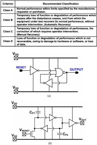
RECOMMENDEDCLASSIFICATIONS OFSYSTEM-LEVELESD TESTRESULTS
Fig. 2. Previous on-chip transient detection circuits composed of (a) latch circuit and (b) capacitors (CP 1and CP 2) to enhance the detection sensitivity.
components may not be integrated into a single chip due to the limitation of chip area and the substantial increase in the total cost of microelectronic products. In the IEC 61000-4-2 standard, four recommended classifications of system-level ESD test re-sults have been defined, as listed in Table II. In order to solve the locked or frozen states caused by system-level ESD zapping, microelectronic products system functions can manually reset with operator intervention, which meets “class C” criterion de-fined in the standard. However, most microelectronic products are required at least to automatically recover the system func-tions without operator intervention to meet “class B” criterion. Therefore, to meet high system-level ESD specifications for mi-croelectronic system products, the chip-level solutions that can help the microelectronic system to execute autorecovery proce-dure without using additional discrete noise-decoupling com-ponents on the printed circuit board (PCB) are highly desired by the IC industry [17], [18].
In previous work, two on-chip transient detection circuits have been proposed to detect transient noise, as shown in Fig. 2(a) and (b). The circuit structure in Fig. 2(a) is composed of a
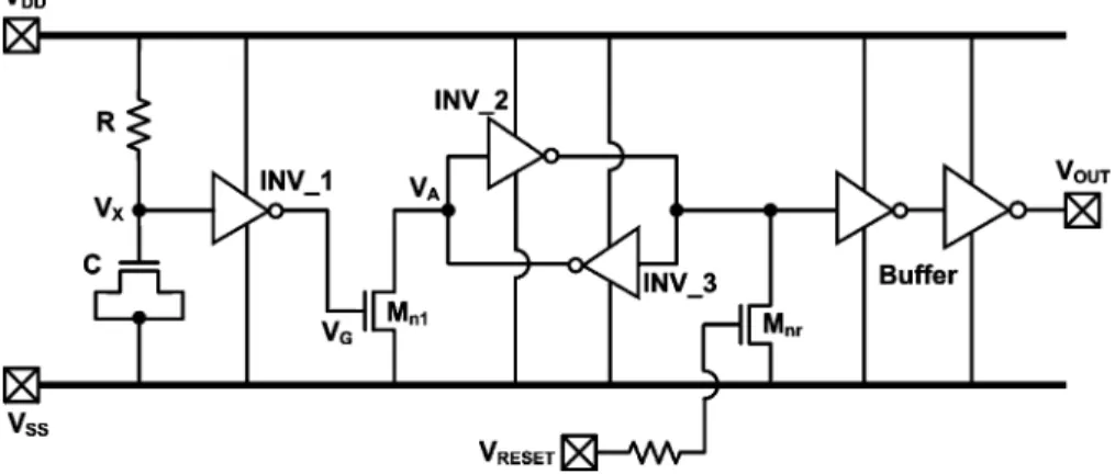
Fig. 3. New proposed on-chip RC-based transient detection circuit.
latch circuit [13]. The detection sensitivity is adjusted by the device ratio between PMOS and NMOS in the latch circuit. The modified design concept in Fig. 2(b) is realized with additional capacitors (CP1 and CP2) located between VD D/VSS power
lines and the input/output nodes of latch circuit to enhance its detection function [17]. However, for both previous designs, the transient detection circuits cannot distinguish the transient noise levels under system-level ESD tests with different ESD voltages.
In this paper, a new on-chip RC-based transient detection cir-cuit is proposed to detect the fast electrical transient under a system-level ESD test. By using a longer time delay in the RC circuit under system-level ESD tests, the proposed new on-chip RC-based transient detection circuit can memorize the occur-rence of system-level ESD events. The circuit operation to detect different positive and negative fast electrical transients has been investigated by HSPICE simulation and verified in silicon. The TLU measurement method [19] and the system-level ESD gun [20] are used to evaluate the detection function of the proposed on-chip RC-based transient detection circuit under system-level ESD test. A novel on-chip transient-to-digital converter com-posed of RC-based transient detection circuits is procom-posed for the first time in the literature to detect the fast electrical transients and convert them to digital thermometer codes under system-level ESD stresses. The experimental results in a 0.18-µm CMOS process with 3.3-V devices have verified that the pro-posed on-chip transient-to-digital converter can successfully convert the fast electrical transients with different ESD voltage levels into digital codes during system-level ESD zapping. In the future works, the proposed on-chip transient-to-digital con-verter can be further co-designed with firmware of self-recovery procedures to provide an effective solution against system-level ESD test in microelectronic systems equipped with CMOS ICs.
II. RC-BASEDTRANSIENTDETECTIONCIRCUIT
A. Circuit Structure
Fig. 3 shows the proposed on-chip RC-based transient detec-tion circuit. The RC-based circuit structure is designed to realize the transient detection function. The two-inverter latch (INV_2 and INV_3) is designed to memorize the logic state before and
after system-level ESD stress. The NMOS (Mnr) is used to
pro-vide the initial reset function to set the initial output voltage (VO U T) level to 0 V. In Fig. 3, the node VXis biased at VD Dand
the node VG is biased at VSS during the normal operation
con-dition. Under the system-level ESD stress, the ESD voltage has a fast rise time on the order of a nanosecond (ns). The voltage level of VXhas a much slower voltage response than the voltage
level at VD D because the RC circuit has a time constant on the
order of a microsecond (µs). Due to the longer delay of the volt-age increase at the node VX, the PMOS device in the inverter1
(INV_1) can be turned on by the overshooting ESD voltage and conducts a voltage to the node VG to further turn on the Mn1
device. The turn-ONMn1device can pull down the output
volt-age level at the node VA. Therefore, the logic level stored in
the two-inverter latch can be changed to detect the system-level ESD event. The output voltage (VO U T) of the proposed on-chip
RC-based transient detection circuit is finally changed from 0 to 3.3 V to memorize the occurrence of system-level ESD events. B. Simulation
From the measured fast electrical transient waveforms shown in the inset in Fig. 1, the underdamped sinusoidal waveforms on VD D and VSSduring the system-level ESD stress have been
observed. Thus, a specific time-dependent voltage source given by
V (t) = V0 + Va sin(2πf (t− td)) exp(−(t − td)Da) (1)
is used to generate an underdamped sinusoidal voltage on the power lines of the proposed on-chip RC-based transient de-tection circuit in the simulation. With the proper parameters such as the applied voltage amplitude Va, initial dc voltage Vo,
damping factor Da, frequency f, and time delay td, the
under-damped sinusoidal voltage can be used for simulation. In the HSPICE simulation with positive or negative underdamped si-nusoidal waveforms, the same parameters of Da = 2× 10⁷s−1,
f= 50 MHz, and td = 500 ns are used (which corresponds to
the measured transient waveform in the inset in Fig. 1). The only difference is that the positive Va is for a positive-going
underdamped sinusoidal waveform and the negative Vais for a
Fig. 4. Simulated VD D, VS S, and VO U T waveforms of the proposed
on-chip RC-based transient detection circuit under system-level ESD test with (a) positive-going and (b) negative-going, overshooting voltages coupled on
VD Dand VS S.
Voof 3.3 and 0 V are used as the initial dc voltages on the VD D
and VSS, respectively, in the simulation.
Under the system-level ESD tests, the transient disturbances on VSS line inside the IC differs from the PCB ground due
to bonding effect in the package and various transmission line effects along the PCB tracks. Therefore, different transient dis-turbances on power lines of CMOS ICs can be induced during system-level ESD tests.
The simulated VD D, VSS, and VO U T waveforms of the
proposed on-chip RC-based transient detection circuit with positive-going and negative-going underdamped sinusoidal voltage on VD D and VSS lines are shown in Fig. 4(a) and (b),
respectively. The positive-going (negative-going) underdamped sinusoidal voltage with amplitude of +8 V (−8 V) is used to simulate the positive (negative) ESD stress under the system-level ESD test. Under ESD stress, VD Dbegins to change rapidly
from normal operation voltage level of 3.3 V. VO U Tis disturbed
simultaneously during the simulated ESD-induced disturbance. During this period, the proposed on-chip RC-based transient
de-Fig. 5. Die photo of the proposed on-chip RC-based transient detection circuits with different RC values in layout.
tection circuit can detect the occurrence of transient disturbance. As a result, after VD Dfinally returns to its normal voltage level
of 3.3 V, VO U Twill be both changed from 0 to 3.3 V, as shown
in Fig. 4(a) and (b).
In this study, a specific time-dependent underdamped sinu-soidal source is used to verify the detection functions of the proposed on-chip transient detection circuit in HSPICE simu-lation. In advance, the interaction between the impedance of the ESD generator and the proposed circuit can be taken into HSPICE simulation to further optimize the circuit operation and design to detect system-level ESD events.
The proposed on-chip RC-based transient detection circuit has been designed and fabricated in a 0.18-µm 1P5M CMOS process with 3.3-V devices. The fabricated chip in a package for system-level ESD test is shown in Fig. 5, where the sili-con area of the proposed on-chip transient detection circuit is 266 µm × 236 µm. The TLU measurement method and the system-level ESD gun are used to evaluate the detection func-tion of the proposed on-chip RC-based transient detecfunc-tion circuit under system-level ESD test.
III. TLU TEST
A. Measurement Setup
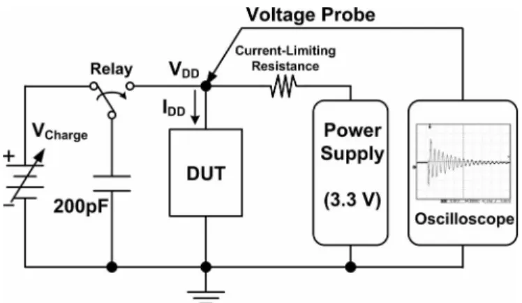
A TLU test has been used to investigate the susceptibility of device under test (DUT) to the noise transient or glitch on the power lines under normal circuit operating condition. The component-level TLU measurement setup with bipolar trigger waveform can accurately simulate the ESD-induced noises on the power lines of CMOS ICs under system-level ESD test [19]. The measurement setup for TLU test is shown in Fig. 6. The charging voltage VC hargehas two different polarities, which are
positive (VC harge > 0) and negative (VC harge < 0). The positive
(negative) VC harge can generate the positive-going
(negative-going) bipolar trigger noise on the power pins of the DUT. A 200-pF capacitor used in the MM ESD test is employed as the charging capacitor. The proposed on-chip RC-based transient detection circuit shown in Fig. 3 is placed as the DUT in Fig. 6. The supply voltage of 3.3 V is used as VD Dand the noise trigger
Fig. 6. Measurement setup for TLU [19].
source is directly connected to DUT through the relay in the measurement setup. The current-limiting resistance is used to avoid electrical overstress (EOS) damage in the DUT under a high-current latchup state. The voltage and current waveforms on the DUT (at VD Dnode) after the TLU test are monitored by
the oscilloscope. B. Measurement Results
Fig. 7(a) and (b) shows the measured VD Dand VO U Ttransient
responses of the proposed on-chip RC-based transient detection circuit under the TLU test with VC hargeof +9 and−2 V,
respec-tively. As shown in Fig. 7(a), under the TLU test with VC harge
of +9 V, VD D begins to increase rapidly from 3.3 V. VO U T is
disturbed simultaneously with positive underdamped sinusoidal voltages on the VD Dpower line. After the TLU test with an
ini-tial VC hargeof +9 V, the output (VO U T) of the proposed on-chip
RC-based transient detection circuit is changed from 0 to 3.3 V. As shown in Fig. 7(b), under the TLU test with VC hargeof−2 V,
VD D begins to decrease rapidly from 3.3 V. VO U T is disturbed
simultaneously with negative underdamped sinusoidal voltages on VD D power line. After the TLU test with an initial VC harge
of −2 V, the output voltage (VO U T) of the proposed on-chip
RC-based transient detection circuit is increased from 0 V to a stable voltage of 3.3 V.
From the TLU test results, the proposed on-chip RC-based transient detection circuit can successfully detect fast electrical transients on the VD D power line. With positive and negative
underdamped sinusoidal voltages on power lines, the output voltages (VO U T) of the proposed on-chip RC-based transient
detection circuit are changed from 0 V to a stable voltage of 3.3 V after the transition.
IV. SYSTEM-LEVELESD TEST
A. Measurement Setup
In the IEC 61000-4-2 standard [10], the equipment specifica-tions for different testing modes have been defined. For tabletop equipment, the measurement setup should consist of a wooden table, standing on the ground reference plane (GRP). Horizontal or vertical coupling planes (VCPs) should be placed on the ta-ble. An insulating plane of 0.5 mm thickness should be inserted
Fig. 7. Measured VD Dand VO U Twaveforms on the proposed on-chip
RC-based transient detection circuit under TLU test with VC h a rg eof (a) +9 V and
(b)−2 V.
between the EUT/cables and horizontal coupling plane (HCP). For floor-standing equipment, the EUT and cables should be isolated from the GRP by an insulating support about 0.1 m thick. Any mounting feet associated with the EUT should be remained in the place. The VCP is used for indirect application of discharges.
In the IEC 61000-4-2 standard [10], two test modes have been also specified, which are the air discharge test mode and the contact discharge test mode. Contact discharge is further di-vided into direct discharge to the system under test, and indirect discharge to horizontal or VCPs. Fig. 8 shows the standard mea-surement setup of the system-level ESD test with the indirect contact discharge test mode. The HCP is connected to the GRP with bleeder wire with two 470-kΩ resistors in series mounded on both ends of the wire. When the ESD gun zaps the HCP, the EMI coming from ESD will be coupled into all CMOS ICs inside EUT. The power lines of CMOS ICs inside EUT will be disturbed by the ESD-coupled energy.
Fig. 8. Measurement setup for a system-level indirect contact ESD zapping to the horizontal coupling plate in the indirect contact discharge test mode [10] to evaluate the detection performance of the proposed on-chip RC-based transient detection circuit.
With such a standard measurement setup, the circuit perfor-mance of the proposed on-chip RC-based transient detection circuit under system-level ESD tests can be evaluated. By using the digital oscilloscope, the transient responses on power lines of CMOS IC products can be recorded and analyzed. Before each system-level ESD zapping, the initial output voltage (VO U T)
of the proposed on-chip RC-based transient detection circuit is reset to 0 V. After each system-level ESD zapping, the output voltage (VO U T) level is measured to check the final voltage level
and verify the detection function. Thus, the circuit performance of the proposed on-chip RC-based transient detection circuit can be directly evaluated with this measurement setup.
B. Measurement Results
The measured VD D and VO U T waveforms of the proposed
on-chip RC-based transient detection circuit under a system-level ESD test with the ESD voltage of +0.2 and −0.2 kV zapping on the HCP are shown in Fig. 9(a) and (b), respectively. Under system-level ESD zapping conditions, VD D line is no
longer maintained at the normal voltage level of +3.3 V. Mean-while, VO U T begins to change under such a high-energy ESD
stress. During the fast transient disturbance, VD D and VO U T
are influenced simultaneously. Finally, the output voltage of the proposed on-chip RC-based transient detection circuit has been changed from 0 to 3.3 V. Therefore, the proposed on-chip RC-based transient detection circuit can sense the fast electri-cal transient on the power lines and memorize the occurrence of system-level ESD events. The experimental result shown in Fig. 9(a) [Fig. 9(b)] is consistent with the HSPICE simulation results in Fig. 4(a) [Fig. 4(b)].
V. TRANSIENT-TO-DIGITALCONVERTER
A. Transient Detection Circuit With On-Chip Noise Filter Network
It has been shown that noise filter networks can enhance im-munity of CMOS ICs to system-level ESD test by decoupling,
Fig. 9. Measured VD Dand VO U T transient voltage waveforms of the
pro-posed on-chip RC-based transient detection circuit under system-level ESD test with ESD voltage of (a) +0.2 kV and (b)−0.2 kV.
Fig. 10. On-chip RC-based transient detection circuit combined with a noise filter network.
bypassing, or absorbing ESD-induced noise voltage (energy). It has also been reported that the noise filter networks have strong impact to the parameters of the underdamped sinusoidal voltage such as transient peak voltage, damping frequency, and damping factor [15]. Fig. 10 shows the on-chip RC-based tran-sient detection circuit combined with a RC filter network, which is realized with one decoupling capacitor and two resistors with equal value to provide the noise filter function during system-level ESD stresses. The RC noise filter network can suppress the transient peak voltages on VD D and VSS, which influences
positive and negative system-level ESD voltages to cause tran-sition at the output (VO U T) of the proposed on-chip RC-based
transient detection circuit. Therefore, in combination with dif-ferent RC noise filter networks, the proposed on-chip RC-based transient detection circuit can be designed to detect different voltage levels under system-level ESD tests.
The on-chip RC-based transient detection circuit combined with on-chip RC filter network has been designed and fabricated in a 0.18-µm 1P5M CMOS process with 3.3-V devices.
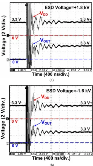
With the aid of the on-chip filter network to reduce the noise voltage on power lines, the minimum positive system-level ESD voltage to cause transition at the output (VO U T) of the proposed
on-chip RC-based transient detection circuit can be significantly enhanced from +0.2 kV (without on-chip filter network) to +1.8 kV (with on-chip filter network), as shown in Fig. 11(a). Similarly, the minimum negative system-level ESD voltage to cause transition at the output (VO U T) of the proposed on-chip
RC-based transient detection circuit can be also enhanced from −0.2 kV (without chip filter network) to −1.6 kV (with on-chip filter network), as shown in Fig. 11(b). Thus, by choosing proper capacitance and resistance, the on-chip filter network placed between VD Dand VSScan be used to appropriately adjust
the detection voltage level of the proposed on-chip RC-based transient detection circuit under system-level ESD test, both for the positive or the negative electrical fast transients. With different detection voltage levels, the strength of system-level ESD stress to the CMOS ICs can be converted into digital codes. Therefore, a novel transient-to-digital converter can be built up by using the proposed on-chip RC-based transient detection circuits with different RC filter networks.
B. Four-Bit Transient-to-Digital Converter
Fig. 12 shows the proposed on-chip transient-to-digital con-verter. The 4-bit on-chip transient-to-digital converter consists
Fig. 11. Measured VD Dand VO U T transient voltage waveforms of the
pro-posed on-chip RC-based transient detection circuit combined with a noise filter network under a system-level ESD test with an ESD voltage of (a) +1.8 kV and (b)−1.6 kV.
of four RC-based transient detection circuits with four different RC filter networks. With different resistance values in the filter networks, different ESD energy on VD Dand VSSwill reach each
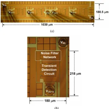
transient detection circuit. Therefore, under the system-level ESD zapping conditions with different ESD voltages, the four transient detection circuits will have different output responses. The proposed on-chip transient-to-digital converter has been de-signed and fabricated in a 0.18-µm 1P5M CMOS process with 3.3-V devices. The fabricated chip in a package for system-level ESD test is shown in Fig. 13(a) and (b). The silicon area of pro-posed on-chip 4-bit transient-to-digital converter is 1030 µm× 188.5 µm, as shown in Fig. 13(a). The silicon area of detection circuit to generate 1-bit output signal is 218 µm× 180 µm, as shown in Fig. 13(b).
The measured VO U T 1, VO U T 2, VO U T 3, and VO U T 4
wave-forms of the proposed on-chip transient-to-digital converter un-der system-level ESD test with an ESD voltage of +0.8 kV zapping on the HCP are shown in Fig. 14(a). During the fast transient of the ESD stress, VO U T 1, VO U T 2, VO U T 3, and VO U T 4
are disturbed simultaneously during the VD D and VSS
Fig. 12. Proposed on-chip 4-bit transient-to-digital converter realized with four transient detection circuits and RC filter networks.
Fig. 13. Die photos of: (a) whole 4-bit transient-to-digital converter realized with four transient detection circuits and RC filter networks, and (b) detection circuit to generate the VO U T 4signal.
VO U T 2, VO U T 3, and VO U T 4 remain 0 V. Therefore, under a
system-level ESD test with an ESD voltage of +0.8 kV zapping, the output voltages of the proposed on-chip transient-to-digital converter can be transferred into a digital thermometer code of “0001.”
Similarly, Fig. 14(b), (c), and (d) shows the measured VO U T 1, VO U T 2, VO U T 3, and VO U T 4 waveforms of the
pro-posed on-chip transient-to-digital converter under a system-level ESD test with ESD voltages of +1.2, +1.8, and +3.1 kV zap-ping on the HCP, and transferred into digital thermometer codes of “0011,” “0111,” and “1111,” respectively.
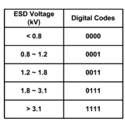
Fig. 15 depicts the relationship between the ESD zapping voltages and the converted codes. With the proposed on-chip transient-to-digital converter, different ESD voltages un-der system-level ESD tests can be detected and transferred into different digital thermometer codes. With a larger ESD volt-age level, the digital thermometer code goes higher, as listed in Table III.
VI. FUTUREWORKS ANDAPPLICATIONS
It had been reported that the hardware/firmware can be co-designed to effectively improve the system-level ESD
Fig. 14. Measured VO U T 1, VO U T 2, VO U T 3, and VO U T 4 transient voltage waveforms of the proposed on-chip 4-bit transient-to-digital converter under a
system-level ESD test with an ESD voltage of (a) +0.8 kV, (b) +1.2 kV, (c) +1.8 kV, and (d) +3.1 kV, zapping on the HCP.
Fig. 15. Relationship between the ESD zapping voltage and the digital code in the proposed transient-to-digital converter.
robustness of CMOS IC products [13]. The proposed on-chip transient-to-digital converter can be further co-designed with firmware to provide a system solution to solve the system-level ESD event to microelectronic products equipped with CMOS ICs.
To realize a system-level ESD protection of a function against upset or freeze after transition, a hardware/firmware
co-TABLE III
ESD VOLTAGE TODIGITALCODECHARACTERISTIC
design solution combined with the proposed on-chip transient-to-digital converter and the power-ONreset circuit can be built up. Under the normal power-ONcondition, the VD D power-ON
voltage waveform has a rise time on the order of a millisec-ond (ms). The power-ONreset circuit should be designed with the longer rise time on the order of millisecond. Thus, the out-put signal of the power-ONreset circuit can send the power-on
Fig. 16. Hardware/firmware operation during (a) power-ONreset condition, (b) low system-level ESD zapping, and (c) high system-level ESD zapping.
firmware index for a microelectronic system to execute a normal reset procedure, as shown in Fig. 16(a).
Due to the difference in the rise times between the ESD zapping voltage and the VD D power-ONvoltage, the proposed
on-chip transient-to-digital converter is designed to sense fast electrical transients and send different output digital codes un-der the system-level ESD zapping conditions with different ESD voltages, as shown in Fig. 16(b) and (c). For example, under the system-level ESD zapping with a low ESD voltage, the output digital code of the proposed on-chip transient-to-digital con-verter becomes “0001.” Then, the firmware can execute the partial system recover procedure to check and recover par-tial electrical functions of microelectronic system. Under the system-level ESD zapping with high enough ESD voltage, the output digital code of the proposed on-chip transient-to-digital converter becomes “1111.” Then, the firmware can execute the recover procedure to recover all the electrical functions to a desired stable state as soon as possible. The firmware can be
designed to execute different recover procedures with different output digital codes of the proposed on-chip transient-to-digital converter. After the reset and recover procedures, the output dig-ital code of the proposed on-chip transient-to-digdig-ital converter is again reset to “0000” for detecting the next transient ESD events.
By including the proposed on-chip transient-to-digital con-verter and an additional firmware index into the chip, the firmware flowchart shown in Fig. 16(a)–(c) can be used to im-prove the system-level ESD robustness of microelectronic prod-ucts. At this moment, different self-recovery procedures based on the proposed transient-to-digital converter under different ESD stress levels have not been supported by simulations or ex-perimental test chips. The output digital codes generated from transient-to-digital converter for using as the firmware index to execute different self-recovery procedures in microelectronic systems will be implemented in some real IC products in the future.
output digital thermometer codes of the proposed transient-to-digital converter can successfully correspond to the different ESD voltages under system-level ESD tests. The proposed on-chip transient-to-digital converter can be further combined with firmware cooperation to provide an effective solution against upset or freeze malfunctions after system-level ESD zapping on microelectronic systems.
ACKNOWLEDGMENT
The authors would like to thank Mr. C.-C. Tsai and Dr. T.-Y. Chen for their valuable technical discussions and the project support from Himax Technologies, Inc., Taiwan. The authors would also like to thank the Associate Editor, Dr. A. Duffy, and his reviewers for their valuable suggestions and comments to improve this paper.
REFERENCES
[1] S. Voldman, ESD: Circuits and Devices. New York: Wiley, 2006. [2] A. Amerasekera and C. Duvvury, “The impact of technology scaling on
ESD robustness and protection circuit design,” in Proc. EOS/ESD Symp., 1994, pp. 237–245.
[3] C. Diaz, T. Kopley, and P. Marcoux, “Building-in ESD/EOS reliability for sub-half-micron CMOS processes,” in Proc. IEEE Int. Rel. Phys. Symp.
(IRPS), 1995, pp. 276–283.
[4] Electrostatic Discharge Sensitivity Testing—Human Body Model (HBM)—
Component Level, ESD Association Standard, Test Method ESD STM5.1,
2001.
[5] Electrostatic Discharge Sensitivity Testing—Machine Model (MM)—
Component Level, ESD Association Standard, Test Method ESD STM5.2,
1999.
[6] S. Daniel and G. Krieger, “Process and design optimization for advanced CMOS I/O ESD protection devices,” in Proc. EOS/ESD Symp., 1990, pp. 206–213.
[7] R. Rountree, “ESD protection for submicron CMOS circuits: Issues and solutions,” in IEDM Tech. Dig., 1988, pp. 580–583.
[8] M.-D. Ker, “Whole-chip ESD protection design with efficient VDD-to-VSS clamp circuit for submicron CMOS VLSI,” IEEE Trans. Electron
Devices, vol. 46, no. 1, pp. 173–183, Jan. 1999.
[9] M.-D. Ker and S.-F. Hsu, “Physical mechanism and device simulation on transient-induced latchup in CMOS ICs under system-level ESD test,”
IEEE Trans. Electron Devices, vol. 52, no. 8, pp. 1821–1831, Aug.
2005.
[10] EMC—Part 4-2: Testing and Measurement Techniques—Electrostatic
Dis-charge Immunity Test, International Standard IEC 61000-4-2, 2001.
[11] N. Shimoyama, M. Tanno, S. Shigematsu, H. Morimura, Y. Okazaki, and K. Machida, “Evaluation of ESD hardness for fingerprint sensor LSIs,” in
Proc. EOS/ESD Symp., 2004, pp. 75–81.
[12] D. Smith and A. Wallash, “Electromagnetic interference (EMI) inside a hard disk driver due to external ESD,” in Proc. EOS/ESD Symp., 2002, pp. 32–36.
[13] M.-D. Ker and Y.-Y. Sung, “Hardware/firmware co-design in an 8-bits microcontroller to solve the system-level ESD issue on keyboard,”
Mi-croelectron. Rel., vol. 41, no. 3, pp. 417–429, Mar. 2001.
[14] M. Montrose, Printed Circuit Board Design Techniques for EMC
Compli-ance. Piscataway, NJ: IEEE Press, 2000.
[15] M.-D. Ker and S.-F. Hsu, “Evaluation on board-level noise filter networks to suppress transient-induced latchup in CMOS ICs under system-level
[19] M.-D. Ker and S.-F. Hsu, “Component-level measurement for transient-induced latch-up in CMOS ICs under system-level ESD considerations,”
IEEE Trans. Device Mater. Rel., vol. 6, no. 3, pp. 461–472, Sep. 2006.
[20] Electrostatic Discharge Simulator, NoiseKen ESS-2002 & TC-825R, Noise Laboratory Co., Ltd. Sagamihara, Japan, 2004.
Ming-Dou Ker (S’92–M’94–SM’97–F’08) received
the Ph.D. degree from the Institute of Electronics, National Chiao-Tung University, Hsinchu, Taiwan, in 1993.
He was a Department Manager in the Very Large Scale Integration (VLSI) Design Division, Computer and Communication Research Laboratories, Indus-trial Technology Research Institute (ITRI), Hsinchu, Taiwan. Since 2004, he has been a Full Professor in the Department of Electronics Engineering, National Chiao-Tung University. From 2006 to 2008, he was the Director of Master’s Degree Program with the College of Electrical Engi-neering and Computer Science, National Chiao-Tung University, as well as the Associate Executive Director of National Science and Technology Program on System-on-Chip (NSoC), Taiwan. Since 2008, he has been the Chair Professor and the Vice President of I-Shou University, Kaohsiung, Taiwan, by rotation. In the field of reliability and quality design for circuits and systems in CMOS technology, he has authored or coauthored over 360 technical papers in interna-tional journals and conferences. He has proposed many inventions to improve the reliability and quality of ICs, which have been granted with 139 U.S. patents and 144 R.O.C. (Taiwan) patents. He had been invited to teach and/or to con-sult the reliability and quality design for IC products by hundreds of design houses and semiconductor companies in the worldwide IC industry. His current research interests include reliability and quality design for nanoelectronics and gigascale systems, high-speed and mixed-voltage I/O interface circuits, on-glass circuits for system-on-panel applications, and biomimetic circuits and systems for intelligent prosthesis.
Prof. Ker has served as a member of the Technical Program Committee and the Session Chair of numerous international conferences. He served as an Associate Editor for the IEEE TRANSACTIONS ONVLSI SYSTEMS. He has been selected as a Distinguished Lecturer in the IEEE Circuits and Systems Soci-ety (2006–2007) and in the IEEE Electron Devices SociSoci-ety (2008–2009). He was the President of Foundation in Taiwan ESD Association. In 2009, he was awarded as one of the top ten Distinguished Inventors in Taiwan and one of the top 100 Distinguished Inventors in China.
Cheng-Cheng Yen (S’07) received the B.S. degree
from the National Chiao-Tung University, Hsinchu, Taiwan, in 1998, and the M.S. degree from the In-stitute of Electronics, National Chiao-Tung Univer-sity, where he is currently working toward the Ph.D. degree.
His research interests include transient detection circuits and IC reliability design to meet system-level EMC/electromagnetic susceptibility (EMS) regulations.

![Fig. 8. Measurement setup for a system-level indirect contact ESD zapping to the horizontal coupling plate in the indirect contact discharge test mode [10] to evaluate the detection performance of the proposed on-chip RC-based transient detection circuit.](https://thumb-ap.123doks.com/thumbv2/9libinfo/7969904.158480/6.891.190.694.100.373/measurement-horizontal-indirect-discharge-detection-performance-transient-detection.webp)