國
立
交
通
大
學
電子物理學系
博 士 論 文
氧化鉿閘極介電層之氟鈍化製程與應力工程的研究
Study on Fluorine Passivation Techniques and Strain
Engineering for HfO
2Gate Dielectrics
研 究 生:吳偉成
指導教授:趙天生 教授
賴朝松 教授
氧化鉿閘極介電層之氟鈍化製程與應力工程的研究
Study on Fluorine Passivation Techniques and Strain
Engineering for HfO
2Gate Dielectrics
研 究 生: 吳偉成 Student:Woei-Cherng Wu
指導教授: 趙天生 Advisor:Tien-Sheng Chao
賴朝松 Chao-Sung Lai
國 立 交 通 大 學
電子物理學系
博 士 論 文
A DissertationSubmitted to Department of Electrophysics College of Science
National Chiao Tung University in partial Fulfillment of the Requirements
for the Degree of Doctor of Philosophy
in Electrophysics
March 2008
Hsinchu, Taiwan, Republic of China
氧化鉿閘極介電層
之
氟鈍化製程與應力工程的研究
學生: 吳偉成 指導教授: 趙 天 生 博士
賴 朝 松 博士
國 立 交 通 大 學 電 子 物 理 學 系 博 士 班
摘要
首先,我們提出多種氟鈍化(passivatation)技術以製作高效能且高可靠度的二 氧化鉿閘極絕緣層(HfO2 gate dielectrics)。接著研究經過氟化之氧化鉿其電流穿遂機制(current transportation mechanism)與載子捕捉(charge trapping)特性。最後, 我們發現氮化矽所引發的應力(strain)矽通道之氧化鉿電晶體,其可靠度以及元件 特性都獲得大幅度的改善
一 開 始 我 們 提 出 了 以 矽 表 面 氟 離 子 植 入 法(silicon surface fluorine implantation),將氟離子導入二氧化鉿薄膜以及此二氧化鉿薄膜與矽基板之介面 處。從實驗結果可以充分證明此氟化二氧化鉿薄膜會擁有較好的熱穩定性,此氟 化二氧化鉿薄膜的漏電流會比一般傳統的二氧化鉿還低了三個數量級,此外,應 力下所導致的漏電流(stress-induced leakage current)以及電荷捕捉(charge trapping) 的問題都可以藉由此氟離子佈值法來使得此二氧化鉿閘極介電層有更好的特 性。此氟原子與二氧化鉿薄膜混合不僅僅可以減少介面狀態的懸空鍵結(interface dangling bond)還可以有效減少此薄膜層的電荷捕捉情形,而進一步的有效改善二 氧化鉿薄膜的特性。另ㄧ方面,我們進一步研究氟化氧化鉿閘極介電層其電流傳 導機制。我們利用變溫量測的漏電流變化以及低溫(77 K)量測的漏電流來分析電 流傳導特性以及此電容元件的能帶圖(energy band diagrams),從實驗結果中可以 發現氟化介面層與矽基板的傳導帶落差(conduction band offset)有3.2 eV而傳統介 面層的落差則只有2.7 eV;氟化二氧化鉿與金屬閘極的傳導帶落差有2.6 eV而傳 統二氧化鉿的落差則只有1.9 eV;不論是閘極注入(gate injection)模式或基板注入 (substrate injection)模式操作,氟化二氧化鉿的有效載子捕捉深度大約是低於介電
層傳導帶1.25 eV,而傳統的二氧化鉿在閘極注入模式下的有效載子捕捉深度大 約是低於介電層傳導帶1.04 eV,而在基板注入模式下的有效載子捕捉深度大約 是低於介電層傳導帶1.11 eV。 此外,我們提出與現有製程具高度匹配性的四氟化碳電漿處理(CF4 plasma treatment)技術,用以製作高效能的二氧化鉿閘極絕緣層之電容。此技術可分類 成兩種:首先藉由前處理的技術,我們可以有效的抑制高介電閘極絕緣層電容中 的介面層(interfacial layer)生長,藉此得到更薄的等效氧化層厚度(effective oxide thickness),除此之外,還可以有效的抑制矽化鉿的形成並產生鉿-氟鍵結(Hf-F bonding)。接著利用四氟化碳電漿後處理的技術,氟原子可以有效地被導入二氧 化鉿薄膜以及此二氧化鉿薄膜與矽基板之介面以消除薄膜中的載子補獲態(trap states),並進而有效地改善此閘極絕緣層的介面特性。經由四氟化碳電漿處理的 二氧化鉿閘極絕緣層之電容具有較低的漏電流、高的崩潰電壓及較薄的等效氧化 層厚度(effective oxide thickness);其磁滯現象(hysteresis)更大幅改善了超過 90 %。此外,我們更進一步提出物理模型來解釋此磁滯效應的改善機制。 接著我們提出新穎之氟化氧化鉿電晶體,利用四氟化碳電漿處理,可同時改 善n型及p型氧化鉿電晶體,相當適用於新型互補式金氧半場效電晶體的製作。此 電晶體有相當高水準的表現及可靠度:高達6.69×10⁷的導通電流與關閉電流之比 例、 接近76 mV/dec的次臨界擺幅、小於20 mV的源極引發能障衰退以及相當高 的載子遷移率(~165 cm2/V.s)。此氟化氧化鉿電晶體有較佳的介面特性及品質較
好的絕緣層:較小的閘極引發汲極漏電流(gate induced drain leakage)以及較低的 正偏壓溫度所引起的元件不穩定性。而造成此特性及可靠度改善的原因是來自於 氟原子導入二氧化鉿薄膜以及此二氧化鉿薄膜與矽基板之介面,進一步減少介電 層的缺陷且抑制電子電洞對的產生,並導致絕緣層有較深的載子捕捉位置及減少 載子捕捉情形的發生。 最後,我們首度對於氮化矽所引發的應變矽通道之氧化鉿電晶體提出新的發 現,可靠度以及元件特性都獲得大幅度的改善,此外,我們利用脈衝型量測系統 去分析此氧化鉿電晶體接近真實的特性,發現有百分之九十的驅動電流增加以及 百分之五十的轉移電導的提升。而此應變矽通道的氧化鉿電晶體會擁有較佳的介 面特性以及較低的正偏壓溫度所引起的元件不穩定性,其元件的充電電流泵 (charge pumping current)有大約百分之九十的減少且正偏壓溫度所引起的元件不 穩 定 性 效 應 也 降 低 了 百 分 之 五 十 五 。 之 後 我 們 利 用 動 態 臨 限 電 壓(dynamic threshold)操作法來提升應變矽通道的氧化鉿電晶體的元件特性,發現轉移電導有
高達百分之ㄧ百三十五的增加,且次臨界擺幅有接近理想的表現(~62 cm2/V.s),
Study on Fluorine Passivation Techniques and Strain
Engineering for HfO2 Gate Dielectrics
Student: Woei Cherng Wu Advisor: Dr. Tien-Sheng Chao
Dr. Chao-Sung Lai
Department of Electrophysics, National Chiao Tung University
Abstract
First, we demonstrated several fluorine passivation technologies to fabricate high performance and highly reliable HfO2 gate dielectrics. Then, we investigated the
current transportation and charge trapping mechanism of fluorinated HfO2 gate
dielectrics. Finally, new observation on improved characteristics and PBTI reliability of contact etching stop layer induced local tensile strained nMOSFETs with HfO2 gate
dielectrics were reported
At beginning, we describe the characteristics of silicon surface fluorine implantation (SSFI) for HfO2 films with high-temperature postdeposition annealing.
The thermal stability of HfO2 gate dielectrics is much improved owing to the
incorporation of fluorine into HfO2 thin films. The gate leakage current of the SSFI
HfO2 films is about three orders less than that of samples without any fluorine
implantation. In addition, improvements in stress-induced leakage current (SILC) and charge trapping characteristics are realized in the HfO2 films with the SSFI. The
incorporation of fluorine atoms into the HfO2 films reduces not only interface
dangling bonds but also bulk traps, which is responsible for the improvements in properties. On the other hand, the current transportation mechanism of HfO2 gate
dielectrics with TaN metal gate and silicon surface fluorine implantation (SSFI) is also investigated. Based on the experimental results of the temperature dependence of gate leakage current and Fowler–Nordheim tunneling characteristics at 77 K, we have extracted the current transport mechanisms and energy band diagrams for TaN/HfO2/IL/Si structures with fluorine incorporation, respectively. In particular, we
barrier heights (or conduction band offset): 3.2 eV & 2.7 eV; ii) TaN/ fluorinated and as-deposited HfO2 barrier height: 2.6 eV & 1.9 eV; and iii) effective trapping levels at
1.25 eV (under both gate and substrate injections) below the HfOF conduction band, 1.04 eV (under gate injection) and 1.11 eV (under substrate injection) below the HfO2
conduction band, which contributes to Frenkel–Poole conduction.
In addition, a process-compatible CF4 plasma treatment for fabricating
high-performance HfO2 gate dielectrics MOS capacitor is demonstrated. This CF4
plasma treatment was divided into two parts, which are pre-CF4 plasma treatment and
post-CF4 plasma treatment, respectively. The effective oxide thickness of high-k gate
dielectrics was much reduced by using the pre-CF4 plasma treatment due to the
elimination of the interfacial layer between HfO2 and Si-substrate. In addition, the
Hf-silicide was suppressed and Hf-F bonding was observed for the CF4 plasma
pre-treated sample. On the other hand, the fluorine atoms were effectively incorporated into HfO2 thin film and HfO2/Si interface by post-CF4 plasma treatment.
The charge trapping would be eliminated and the interface of the HfO2 gate dielectrics
was also improved. The device post-treated by CF4 plasma treatment would have low
leakage current, higher breakdown voltage, and thinner effective oxide thickness. Besides, the C-V hysteresis was much reduced about 90 %. A physical model was presented to explain the improvement of hysteresis phenomenon and the elimination of charge trapping of the fluorinated HfO2 gate dielectrics.
Then, a novel high-performance and excellent-reliability HfOF MOSFET was demonstrated. Both n and p-type HfOF MOSFET can be improved by CF4 plasma
treatment, indicating this technique is compatible with CMOS fabrication. Large
ION/Imin current ratio (~6.69×10⁷), good Subthreshold Swing (~76 mV/dec), small
DIBL (<20 mV), and high mobility (~165 cm2/V.s) can be observed for the HfOF nMOSFETs. The HfOF nMOSFET has better HfO2/Si interface and dielectric quality,
including small GIDL current and less PBTI effect. Reduced GIDL current was observed for the HfOF nMOSFET due to HfO2/Si interface passivation by fluorine,
resulting in less hole-electron pair generation. The fluorine incorporation into HfO2
gate dielectrics effectively passivated the dielectric vacancies, resulting in a deeper trapping cross section and a lower concentration of generated traps.
Finally, new observation on SiN-cap strain-induced improved characteristics and PBTI reliability of nMOSFETs with HfO2 gate dielectrics were reported for the first
SiN-capped HfO2 nMOSFETs were much enhanced about 90% and 50%, respectively
by pulse-IV measurement. The CESL-device has better HfO2/Si interface and
dielectric quality, including less charge pumping current (90% reduction) and less PBTI effect (55% reduction). Finally, the performance of CESL-HfO2 nMOSFETs
will have larger gm (135% increase) and “close-to-ideal” subthresold swing (~62)
using dynamic threshold (DT) operation mode with tolerant hot carrier-stress characterization. These results provide a valuable guideline for the future 45 nm and beyond CMOS device design with high-k and strain engineering.
誌謝
畢業了!從沒想過會念博士班的我也畢業了,首先要感謝我的指導教授趙天 生博士在這個領域上給我的指導與幫助,從老師身上也讓我看到了身為一個學者 該有的風範,老師的一句話:「家庭就是我們最大的事業」,學生將永遠謹記在心 並奉為圭臬。另外,我還要感謝共同指導教授賴朝松博士。賴老師對我來說,是 亦師亦友。把我從大學時期愛玩的心調教成對研究的熱情,老師耐心一字一句的 教導我寫第一篇國際會議論文讓我相當感動且獲益匪淺,在此衷心感謝兩位老師 對學生不辭辛勞的指導。 感謝從我碩士班求學期間就帶我、指導我的王哲麒學長。因為有王哲麒學長 對我的許多指導與幫助,讓我成長了很多,學長在學術實驗上嚴謹的態度及深厚 的理論基礎是我最推崇的,無私的指導學弟更讓我學得如何當一位學長。也感謝 我帶過的幾位學弟:武欽、德馨、子銘、冠迪、時璟,這本論文是我們一起努力 的成果。感謝陪我渡過漫長求學路的實驗室成員們:建豪學長、柏儀學長、家豪 學長、小馬、宗宜、阿邦、慶譚、俊祥、彥學、小棟、佩珊、高興、宗諭、美君、 小宗育、智盟、意宏,你們讓我在學校的生活更加多采多姿。相信不久之後在職 場中,我們會再相遇的。 要感謝的,還有一群交心的麻吉幫兄弟:百騏(百娘)、弘彬(娘彬)、奕臺 (娘臺)、文政(軟政)、克竣(克軟)、智維(志雄)、厚耕(蠢蛋)、佑聰(side)、 緒寬(血壓),和你們的兄弟聚會,是我最輕鬆、最快樂的時光。在我學業跟感情 低潮那時,能夠遇到你們這群交心的好兄弟,是我最開心也最珍惜的一件事!更 感謝在我漫長求學期間一直陪在我身邊的小晏,妳是我念博士班最大的動力,有 了妳我才能夠順利將論文完成。妳除了豐富我的感情生活外,也讓我能夠用更成 熟、更自省的心態去完善我以後的感情與人生。 最後,謹以這本博士論文,獻給我的爸媽,沒有你們無怨無悔的犧牲奉獻, 不會有今日的我。還有我的妹妹。我的成就,因為有你們,一切才具有了意義。 你們永遠都是我最愛的家人! 2008 于 風城․交大CONTENTS
ABSTRACT (in Chinese)
………..IABSTRACT (in English)
………IIIACKNOWLEDGEMENT
……….VICONTENTS
………...VIITABLE CAPTIONS
……….XIFIGURE CAPATIONS
………..XIIChapter 1 Introduction
……….11.1 Background………..1
1.2 Motivation………3
1.3 Organization of the thesis……….4
Chapter 2 Characteristics of HfO
2Gate Dielectrics with Fluorine
Implantation
………..92-1 Characteristics of Fluorine Implantation for HfO2 Gate Dielectrics with High Temperature Annealing………9
2-1.1 Introduction………...9
2-1.2 Experiment………...10
2-1.3 Results and Discussion……….…..11
2-1.4 Summary……….14
2-2 Current Transport Mechanism of TaN/HfO2/IL/Si Structure with Silicon Surface Fluorine Implantation (SSFI)………...24
2-2.1 Introduction………...…..24
2-2.3 Results and Discussion………..………...…..27
2-2.4 Summary………...……..32
Chapter 3 Effects of CF
4Plasma Treatment on the Ultra-Thin HfO
2Thin Film
……….433-1 Suppression of Interfacial Reaction for HfO2 on Silicon by Pre-CF4 Plasma Treatment……….43
3-1.1 Introduction………...43
3-1.2 Experiment………...44
3-1.3 Results and Discussion...………....45
3-1.4 Summary……….47
3-2 High Performance HfO2 Gate Dielectrics Fluorinated by Post-deposition CF4 plasma treatment….………51
3-2.1 Introduction……….51
3-2.2 Experiment………..52
3-2.3 Results and Discussion………...54
3-2.4 Summary……….58
Chapter 4 Improvement of CMOS HfO
2Reliability by
Post-deposition CF4 Plasma Treatment
………...……...654-1 Improvement of Positive Bias Temperature Instability (PBTI) of HfO2 nMOSFETs Post-deposition CF4 Plasma Treatment………65
4-1.1 Introduction………...65
4-1.2 Experiment……….…….66
4-1.4 Summary………74
4-2 Improved Characteristics of HfO2 pMOSFETs Post-deposition CF4 Plasma Treatment……….……91
4-2.1 Introduction……….………...91
4-2.2 Experiment……….……….93
4-2.3 Results and Discussion……….…..94
4-2.4 Summary……….………98
Chapter 5 Characteristics of Contact Etch Stop Layer (CESL)
Induced Local Strained HfO
2nMOSFETs
……….1065-1 Performance and Reliability Characteristics for Contact Etch Stop Layer (CESL) Induced Local Strained HfO2 nMOSFETs Using Pulse-IV Analysis……….106
5-1.1 Introduction………...106
5-1.2 Experiment………107
5-1.3 Results and Discussion……….108
5-1.4 Summary………...111
5-2 A Novel Dynamic Threshold HfO2 nMOSFETs (DTMOS) with Local Tensile Strained Channel………...122
5-2.1 Introduction………...122
5-2.2 Experiment………....123
5-2.3 Results and Discussion……….123
5-2.4 Summary………...126
Chapter 6 Conclusions and Recommendations for Future Works
...1336.2 Recommendations for Future Works………...135
References
………..137Publication List
………153Table Captions
Chapter 3
Table 3.1 Summaries of the characteristics for all samples. The fluorinated sample exhibits superior properties in EOT, leakage current, breakdown voltage, hysteresis, and charge trapping………64
Figure Captions
Chapter 1
Chapter 2
Fig. 2.1 Key processes use for samples (a) without and (b) with fluorine implantation……….16 Fig. 2.2 SIMS depth profile of MOS structure with fluorine implantation (dose: 1
x 1013 and 1 x 10¹⁵/cm2). The peak value for fluorine is located at the interface of HfO2 and the silicon substrate. The inset shows the TEM of
the MOS structure with fluorine (dose: 1 x 10¹⁵ /cm2) implantation…...17 Fig. 2.3 Physical model for fluorine atom distribution. The fluorine atoms diffuse
into the HfO2 thin film after thermal annealing………...17
Fig. 2.4 XRD data for (a) as-deposited and (b) with fluorine-implanted sample at different PDA temperatures. The sample without fluorine implantation was crystallized after 700℃ PDA………..18 Fig. 2.5 C-V curves for all samples. Positive flat band voltage shift after 900℃ annealing………..19 Fig. 2.6 Thermal stabilities of EOT for all samples. The EOT increase is
markedly smaller in the sample with fluorine implantation………19 Fig. 1.1
Bandgap and band alignment of high-k dielectrics with respect to siliocn……….8 Fig. 1.2
Measured (dots) and simulated (solid lines) tunneling currents in thin-oxide nMOSFETs. The horizontal dashed line indicates a tunneling current level of 1 A/cm2……….8
.
Fig. 2.7 J-V curves (gate leakage current) for all samples. The leakage current was reduced for the sample with fluorine implantation, particularly under the conditions of 900℃ annealing………..20 Fig. 2.8 Gate leakage current densities at VG = VFB -1 V for all samples at
different annealing temperatures. The thermal stability was markedly improved after fluorine implantation………...20 Fig. 2.9 Relationship of thermal stability between gate leakage current density (at
VG = VFB -1 V) and capacitance equivalent oxide thickness for all
samples at the different annealing temperatures………..21 Fig. 2.10 Stress-induce leakage current (SILC) characteristics of as-deposited and
the fluorine-implanted samples under negative current stress (– 1.3 x 10⁻⁴
A/cm2)………..21
Fig. 2.11 Gate leakage current of stress-induce leakage current (SILC) for all samples under constant current stress (– 1.3 x 10⁻⁴ A/cm2)……….22 Fig. 2.12 Charge trapping characteristics of as-deposited and fluorine-implanted
samples under constant current stress (– 1.3 x 10⁻⁴ A/cm2)……….22 Fig. 2.13 Physical models of charge trapping mechanism under constant current
stress for (a) as-deposited and (b) fluorine-implanted samples………...23 Fig. 2.14 The X-ray Photoelectron Spectroscopy (XPS) analysis of the F 1s
electronic spectra of as-deposited and fluorinated samples, TOA angles of 60o and 90o, respectively……….34 Fig. 2.15 The TEM image of TaN/HfO2/IL/Si MOS structure with fluorine
incorporation (F 1E15) with 600oC PDA………....34 Fig. 2.16 Current-Voltage characteristics for the as-deposited and fluorinated HfO2
gate dielectrics with and without PDA under (a) gate and (b) substrate injections……….….35
Fig. 2.17 The relationship between gate leakage current and CET for all samples. The fluorinated HfO2 gate dielectrics have lower leakage current and
CET………..36 Fig. 2.18 The Weibull distribution of gate leakage current, for the as-deposited and
fluorinated HfO2 gate dielectrics under (a)(c) gate and (b)(d) substrate
injections. A good distribution performance of the fluorinated HfO2 gate
dielectrics was observed………...36 Fig. 2.19 Temperature dependence of gate leakage current increase for the (a)(c)
as-deposited and (b)(d) fluorinated HfO2 (with 1E15 SSFI) gate
dielectrics under (a)(b) gate and (c)(d) substrate injections……….37 Fig. 2.20 The effective F-P trapping level for the as-deposited and fluorinated HfO2
gate dielectrics under (a) gate and (b) substrate injections, respectively. The inset figure shows the F-P curve fit for all samples………..38 Fig. 2.21 The physical model of (a)(c) as-deposited and (b)(d) fluorinated gate
dielectrics for F-P conduction under (a)(b) substrate and (c)(d) gate injections………..39 Fig. 2.22 Current-Voltage characteristics at 77 K measuring for the as-deposited
and fluorinated HfO2 gate dielectrics with and without PDA under (a)
gate and (b) substrate injections………...40 Fig. 2.23 The effective F-N barrier height for the as-deposited and fluorinated
HfO2 gate dielectrics under (a) gate and (b) substrate injections,
respectively. The inset figure shows the well FN fitting for all samples……….41 Fig. 2.24 Band diagrams of (a) as-deposited, (b) SSFI (F 1E13) HfO2, (c) SSFI (F
1E14) HfO2, and (d) SSFI (F 1E15) HfO2, with TaN gate extracted from
Chapter 3
Fig. 3.1 SIMS depth profile of the HfO2 gate dielectrics. The fluorine atoms
accumulated mainly at the HfO2/silicon substrate interface after CF4
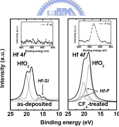
plasma pre-treatment………49 Fig. 3.2 Hf 4f ESCA spectra of (a) as-deposited sample, and (b) CF4 plasma
treated sample, respectively. The inset figures are the fluorine 1s ESCA spectra. A take-off angle (TOA) of 90° was used to measure the ESCA spectra………..49 Fig. 3.3 The C-V characteristics for the samples with and without CF4 plasma
pre-treatment for various HfO2 thin film thicknesses. The inset figures
are the TEM images for the as-deposited and CF4 plasma pre-treated
samples……….50 Fig. 3.4 FTIR spectra of the Si wafers with and without the CF4 plasma treatment.
Whereas the as-deposited sample showed a characteristic native oxide band at 1221 cm-1, the CF4 plasma treated sample did not. The latter
sample had a broader weaker oxide feature at 1180 cm-1 indicating whatever Si-Ox material was present was more amorphous and with
lower surface coverage than in the as-deposited sample……….50 Fig. 3.5 The SIMS depth profile of MOS structure for fluorine oxygen, hafnium
and silicon atoms distribution. The fluorine atoms were accumulated mainly at the two interfaces of the gate-oxide films………59 Fig. 3.6 The chemical analysis (ESCA) spectra of the F 1s electronic spectra of all
samples, respectively, where the F 1s peak is at 687 eV……….59 Fig. 3.7 Hf 4f ESCA spectra of (a) fluorinated and 700oC RTA HfO2 thin films,
and (b) as-deposited and 700oC RTA samples, respectively. A take-off angle (TOA) of 90° was used to measure the ESCA spectra…………...60
Fig. 3.8 The AFM images of the HfO2 thin films surface of (a) without CF4
plasma treatment, and (b) CF4 plasma treatment 1 minute,
respectively………..60 Fig. 3.9 Current-Voltage characteristics for the as-deposited and fluorinated HfO2
gate dielectrics with and without PDA. The inset figure is C-V curves for all samples. The fluorinated HfO2 gate dielectrics have the higher
capacitance and the capacitance would increase after 700℃ annealing for all samples………..61 Fig. 3.10 The relationship between gate leakage current and EOT for all samples.
The fluorinated HfO2 gate dielectrics have both the lower leakage current
and EOT………...61 Fig. 3.11 The Weibull distribution of the (a) gate leakage current and (b)
breakdown voltage, for the as-deposited and fluorinated HfO2 gate
dielectrics. Well distribution performance of fluorinated HfO2 gate
dielectrics was observed……….…..62 Fig. 3.12 The C-V hysteresis characteristics for the (a) as-deposited and (b)
fluorinated HfO2 gate dielectrics, respectively. The inset band-diagram
explains the charge trapping mechanism.………....63 Fig. 3.13 The Weibull distribution of the C-V hysteresis for all samples. Only
50mV C-V hysteresis was observed for the fluorinated HfO2 gate
dielectrics.………....63 Fig. 3.15 Arrhenius plots of leakage current density for the HfO2 and fluorinated
HfO2 gate dielectrics. The plots were obtained from the current-voltage
Chapter 4
Fig. 4.1 C-V curves of the HfO2 nMOSFETs with and without CF4 plasma
treatment………...76 Fig. 4.2 gate leakage currents measured from 303 K to 383 K under gate electron
injection for (a) HfO2 and (b) HfOF gate dielectrics, respectively……..77
Fig. 4.3 Well Frenkel-Poole (F-P) conduction fitting for (a) HfO2 and (b) HfOF
gate dielectrics, respectively………78 Fig. 4.4 Effective F-P barriers at elevated temperature for (a) HfO2 and (b) HfOF
gate dielectrics, respectively………79 Fig. 4.5 ID-VG transfer characteristics of (a) as-deposited and (b) CF4 plasma
treated HfO2 nMOSFETs, where the device channel length and width
were 10 and 100 μm……….80 Fig. 4.6 ID-VD characteristics of as-deposited and CF4 plasma treated HfO2
nMOSFETs, where the device channel length and width were 10 and 100 μm………81 Fig. 4.7 transconductance (gm) extracted from linear region (VD = 0.1 V) for the
as-deposited and fluorinated HfO2 nMOSFETs………...81
Fig. 4.8 ID-VG curves and ISUB current at various drain and gate bias conditions of
(a) as-deposited and (b) CF4 plasma treated HfO2 nMOSFETs………...82
Fig. 4.9 ID-VG curves and ISUB current at various drain and gate bias conditions of
(a) as-deposited and (b) CF4 plasma treated HfO2 nMOSFETs at 70
℃………..83 Fig. 4.10 ID-VG transfer characteristics of (a) as-deposited and (b) CF4 plasma
treated HfO2 nMOSFETs under the same PBTI stress (VG-Vth = 2 V) at
Fig. 4.11 ΔVTH under PBTI stress at different temperatures (RT~100 ℃) for (a)
HfO2 dielectrics and (b) HfOF dielectrics, respectively………..85
Fig. 4.12 ΔVTH afte 1000s PBTI stress at different temperature is quite different
between HfO2 and HfOF gate dielectrics……….86
Fig. 4.13 The GIDL current after 1000s PBTI stress at different temperatures for as-deposited and CF4 treated samples………..86
Fig. 4.14 GIDL mechanism: the electrons tunnel to the drain and contribute to the GIDL current. The holes are swept to the substrate and contribute to the substrate current………...87 Fig. 4.15 Band diagram of suggested GIDL mechanism: GIDL current includes
trap-assisted tunneling and conventional band-to-band tunneling (electron direct tunneling) currents……….87 Fig. 4.16 ID-VG transfer characteristics of (a) as-deposited and (b) CF4 plasma
treated HfO2 nMOSFETs under the same hot carrier (HC) stress (VG-Vth
= 1.5 V, VD = 3 V) at room temperature………..88
Fig. 4.17 ID-VG transfer characteristics of (a) as-deposited and (b) CF4 plasma
treated HfO2 nMOSFETs under the same hot carrier (HC) stress (VG-Vth
= 1.5 V, VD = 3 V) at 50 ℃……….89
Fig. 4.18 ΔVTH under HC-stress at different temperatures (RT~50 ℃) for HfO2
dielectrics and HfOF dielectrics, respectively……….90 Fig. 4.19 The GIDL current after 1000s HC-stress at different temperatures for
HfO2 dielectrics and HfOF dielectrics, respectively………90
Fig. 4.20 C-V curves of the HfO2 pMOSFETs with and without CF4 plasma
treatment……….100 Fig. 4.21 J-V characteristics of the HfO2 pMOSFETs with and without CF4 plasma
Chapter 5
Fig. 5.1 (a) ID-VG and (b) ID-VD characteristics of HfO2 nMOSFETs without and
with different capping nitride thicknesses………..113 Fig. 5.2 The transconductance (gm) increases for conventional and CESL strained
HfO2 nMOSFETs. Inset shows GM increase with gate length decreasing
for HfO2 nMOSFETs……….114
Fig. 4.22 ID-VG transfer characteristics of (a) as-deposited and (b) CF4 plasma
treated HfO2 pMOSFETs, respectively………..101
Fig. 4.23 ID-VD characteristics of as-deposited and CF4 plasma treated HfO2
pMOSFETs, where the device channel length and width were 10 and 100 μm………..102 Fig. 4.24 transconductance (gm) extracted from linear region (VD = 0.1 V) for the
as-deposited and fluorinated HfO2 pMOSFETs………102
Fig. 4.25 ID-VG transfer characteristics of (a) as-deposited and (b) CF4 plasma
treated HfO2 pMOSFETs under the same NBTI stress (VG-Vth = -2 V) at
room temperature………...103 Fig. 4.26 ΔVTH under NBTI stress at different temperatures (RT~70 ℃) for (a)
HfO2 dielectrics and (b) HfOF dielectrics, respectively………104
Fig. 4.27 The GIDL current after 1000s NBTI stress at different temperatures for as-deposited and CF4 treated samples………105
Fig. 4.28 Band diagram of suggested GIDL mechanism: (a) GIDL current includes trap-assisted tunneling and conventional band-to-band tunneling (electron direct tunneling) currents, and (b) fluorine accumulates in HfO2/Si
interface and bulk film, giving interface passivation to reduce trap-assisted tunneling………105
Fig. 5.3 QCP for all samples under different frequencies measuring extracted from
inset figure (Charge pumping characteristics of HfO2 nMOSFETs
without and with different capping nitride thicknesses)………114 Fig. 5.4 Characteristics of VTH shift and GM during 1000s hot carrier (HC) stress
for all samples………115 Fig. 5.5 Driving current degradation after 1000s HC stress for all samples. The
ION degradation is almost the same for all samples………....115
Fig. 5.6 Charge pumping current before and after 1000s HC stress for (a) W/O, and (b) 300 nm CESL devices, respectively. The same ICP increase can be
observed for as-deposited and CESL devices………116 Fig. 5.7 Physical model for CESL-HfO2 nMOSFET under HC stress. HC-stress
only did a little damage on interface near the drain side of CESL-devices……….116 Fig. 5.8 Improved PBTI characteristics can be observed for all CESL-devices.
VTH shift decreases with capping nitride increasing………..117
Fig. 5.9 gm and ION degradation dring 1000s PBTI stress for all samples. Both gm
and ION degradation can be improved for CESL devices………...117
Fig. 5.10 PBTI characteristics (@VG – VTH = 2V) under different temperatures for
all samples. The CESL-devices show obvious temperature dependence……….118 Fig. 5.11 VTH shift increase for CESL-devices after 1000s PBTI stress under high
temperature, indicating deeper oxide trap for CESL-devices…………119 Fig. 5.12 The physical charge trapping model for (a) as-deposited, and (b)
Fig. 5.13 The ID-VD characteristics of (a) 300 nm SiN-capped device under
conventional and pulsed-IV measurement, and (b) all devices under pulsed-IV operation………120 Fig. 5.14 The gm increases with increasing capping nitride thickness for HfO2
nMOSFETs under pulsed-IV measurement. Inset shows ID-VG
characteristics for all samples under pulsed-IV measurement………...121 Fig. 5.15 The ID-VG transfer characteristics of CESL HfO2 nMOSFETs with DT
and normal operations………128 Fig. 5.16 The ID-VD characteristics of CESL HfO2 nMOSFETs with (a) normal and
(b) DT operations………...129 Fig. 5.17 The gm enhancement can be observed for DT operation mode. gm
increases with channel length decreasing for all CESL HfO2 nMOSFETs
under both DT and normal modes………..130 Fig. 5.18 The subthreshold swing can be much improved for all CESL HfO2
nMOSFETs with DT operation mode………130 Fig. 5.19 Characteristics of VTH shift for all CESL HfO2 nMOSFETs with DT
HC-stress. VTH shift is only 105 mV for 300 nm nitride capped device
after 10000 s HC stress………..131 Fig. 5.20 (a) Characteristics of ION degradation for all CESL HfO2 nMOSFETs
with DT HC-stress. ION degradation is only 32% for 300 nm nitride
capped device after 10000 s HC stress………...131 Fig. 5.20 (b) ID-VG curves of all CESL HfO2 nMOSFETs before and after DT
HC-stress. Only ION degradation can be observed after 10000 s HC stress
for all CESL-devices………..132 Fig. 5.21 gm degradation of all CESL HfO2 nMOSFETs during DT
Chapter 1 Introduction
1.1 General Background
Recently, CMOS devices have been aggressively scaled into sub-65 nm regime in order to enhance the device’s performance and increase the integrated circuit functionally. The accelerated downsizing rule of the transistor feature size is to scale the vertical horizontal dimensions simultaneously. With this scaling down, the gate oxide thickness of MOSFETs must be reduced. However, the continuous shrinking of gate dielectrics will face several limitations. According to the ITRS roadmap [1.1], the SiO2 gate dielectric film thickness should be scaled down to 1.0 nm for 45 nm node
technology. Such an ultra-thin SiO2 thin film consists of only a few atomic layers will
cause an unendurable large direct tunneling leakage current. This large direct tunneling current which depends on physical film thickness will cause an intolerable level of off-current, resulting in huge power dissipation and heat.
Figure 1.1 demonstrated the measured and simulated Ig-Vg characteristics under
inversion region for nMOSFET [1.2]. We can see that the gate leakage current will exceed the limit of 1 A/cm2 set by the allowable stand-by power dissipation while the gate oxide thickness scaled down to 2 nm. Further scaling of oxide thickness to below 2 nm, which will cause intolerable power consumption resulted form the increase of large direct tunneling current [1.2]. In addition, the reliability issues will also become an important role for such a thin SiO2 gate dielectric. As a result, a variety of popular
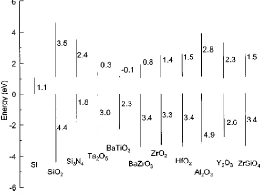
high-k materials such as HfO2, ZrO2, Al2O3, Gd2O3, La2O3, and HfSiON (Hf-silicate)
have been studied as alternative gate dielectrics for 45 nm node and beyond technology to replace the conventional SiO2 or oxynitrides [1.3-1.5]. The electrical
capacitance with a thicker physical thickness by using the high-k gate dielectrics. Figure 1.2 illustrates basic properties of current high-k candidates.
The alternative high-k material should be thermodynamically stable on Si upon high temperature annealing (needed for dopant activation for poly-silicon gates). Unstable dielectrics materials will form interfacial layers, which are between the high-k thin film and silicon substrate. The high-k film and its interfacial layer would affect various device parameters such as EOT, flat band voltage (Vfb), barrier height,
gate leakage current, and channel mobility, and thus significantly affect the transistor behavior. Some of the metal oxides like Ta2O5, TiO2, and BST are known to degrade
when annealed at temperature as low as 600 oC and have poor electrical properties for MOS devices [1.6-1.9]. The newer high-k materials including HfO2, ZrO2, Al2O3,
Y2O3, and lanthanide oxides as well as their silicate and alumunate alloys have
generated a lot of interest primarily due to their potential thermal stability in the presence of Si based on thermodynamic considerations.
To improve the dielectric performance of high-k gate dielectrics, some methods such as deuterium (D2) and forming gas (FG) annealing [1.10-1.11], surface
nitridation pre-treatment [1.12], and formation of the aluminate, silicate and oxynitride [1.13-1.15] alloys, have been investigated recently. It is reported that high-temperature (500 oC~600 oC) post-metal-annealing (PMA) in forming gas prior to metallization improved the channel carrier mobility as well as subthreshold slope of HfO2 MOSFET [1.11]. Unlike the forming gas annealing, the deuterium annealing
provided the hafnium oxide gate dielectrics MOSFET with better reliability characteristics such as threshold voltage (VT) stability under high voltage stress [1.10].
Besides, surface nitridation technique was found effective in preventing boron penetration with a possible drawback of mobility reduction and negative bias temperature instability (NBTI) degradation [1.12]. To further raise the dielectrics
properties, cosputtering of silicon aluminum with hafnium to deposit hafnium silicate and aluminate dielectrics [1.13], and the use of nitric gas for chemical vapor deposition (CVD) [1.14] or oxidizing sputtered metal nitride like HfN to form hafnium oxynitride (HfON) films [1.16], are commonly used.
1.2 Motivation
As the gate oxide thickness scaled continuously, and replacement of the SiO2 or
oxynitride gate film by high-k materials are strongly demanded in order to suppress the direct tunneling current of the gate insulator. NO stack film [1.17], which suppresses the gate leakage current about 1.5 orders of magnitude, could be a good intermediate solution. However, further high-k materials are requested, as the EOT values reduce with downscaling as nearly 0.7 nm [1.18]. Among the candidates shown in Fig. 1.2, HfO2 and its aluminates, silicates or oxynitrides are now the most popular
candidates in recent years.
Nevertheless, there are still various problems to be solved for high-k gate dielectrics before their use in IC technology. First, the poor interface with Si is commonly observed [1.19]. The high-k metal oxides are deposited on the surface of Si and thus do not passivate its surface. This results in a large number of interface traps and charges which is detrimental to metal-oxide-semiconductor (MOS) device performance such as flat band voltage shift and mobility degradation [1.20-1.21]. Second, there is contamination by metal atoms during the deposition of metal oxides (from precursor for CVD) [1.18]. The metal atoms used to form high-k oxides generate deep traps in the silicon band gap. Third, the compatibility of high-k materials with gate electrode needs to be considered [1.22]. Many of the metal oxides mentioned above may not be compatible with traditional gate electrodes used today,
such as poly-Si. The may react with the gate electrode during the subsequent processing and charge its properties, e.g., work function. In addition, one of the main problems is that common high-k dielectrics will crystallize at a fairly low temperature (much less than 900 oC) [1.23]. Crystal grain boundaries then act as high dopant diffusivity paths and may also be the cause of device failure and high leakage. In order to further apply the high-k materials into the CMOS devices, all the problems mentioned above need to be effectively solved.
For the reasons mentioned above, the main purpose of this research is to develop high quality high-k gate dielectrics. CF4 plasma treatment is widely used to improve
the SiO2 gate dielectrics [1.24] and thin film transistor (TFT) [1.25-1.27]. The plasma
treatment processes are also general used in ultra large scale integration (ULSI) technology especially on annealing steps. To further realize the dielectrics properties of these high-k materials, some reliability issues such as hysteresis, charge trapping and temperature dependence are extensively studied. Although the C-V hysteresis mechanism of high-k gate dielectrics has been widely investigated [1.28-1.30], there is still no research about the hystersis phenomenon for the fluorinated high-k gate dielectrics by using CF4 plasma treatment. Besides, the thermal stability of HfO2 gate
dielectrics would be improved for the nitrogen incorporation [1.31-1.33], the characteristics of HfO2 thin film with fluorine incorporation by high temperature
annealing are still not studied. Therefore, the C-V hysteresis phenomenon, charge trapping characteristics, thermal stabilities for the fluorinated HfO2 gate dielectrics by
using the CF4 plasma treatment and fluorine implantation are entirely studied. A
physical model is proposed to well explain the mechanism for electron and hole trapping in fluorinated HfO2 thin film.
There are six chapters in this dissertation. Chapter 1 shows the overview of the high-k gate dielectrics. Motivation for the thesis is also described.
In chapter 2, the improved thermal stability including leakage current, breakdown voltage and thermal stability of the HfO2 gate dielectrics with fluorine
implantation was demonstrated while maintaining the effective oxide thickness (EOT) of 2.5 nm. In addition, the decrease of the stress induce leakage current (SILC) and charge trapping characteristics elimination were also indicated. The reduction of bulk and interface defects by fluorine implantation will contribute to the improved characteristics of HfO2 gate dielectrics.
On the other hand, the current transportation mechanism of HfO2 gate dielectrics
with TaN metal gate and silicon surface fluorine implantation (SSFI) is investigated. Based on the experimental results of the temperature dependence of gate leakage current and Fowler–Nordheim tunneling characteristics at 77 K, we have extracted the current transport mechanisms and energy band diagrams for TaN/HfO2/IL/Si
structures with fluorine incorporation, respectively. In particular, we have obtained the following physical quantities: i) fluorinated and as-deposited IL/Si barrier heights (or conduction band offset): 3.2 eV & 2.7 eV; ii) TaN/ fluorinated and as-deposited HfO2 barrier height: 2.6 eV & 1.9 eV; and iii) effective trapping levels at 1.25 eV
(under both gate and substrate injections) below the HfOF conduction band, 1.04 eV (under gate injection) and 1.11 eV (under substrate injection) below the HfO2
conduction band, which contributes to Frenkel–Poole conduction.
In chapter 3, we discussed that the fluorine atoms were incorporated into HfO2
thin film by CF4 plasma treatment to form the fluorinated HfO2 gate dielectrics. At
first, the effects of pre-CF4 plasma treatment on Si for sputtered HfO2 gate dielectrics
are investigated. The Hf-silicide would be suppressed and Hf-F bonding was observed for the CF4 plasma pre-treated sample. Compared with the as-deposited sample, the
effective oxide thickness was much reduced for the pre-CF4 plasma treated sample
due to the elimination of the interfacial layer between HfO2 and Si-substrate. These
improved characteristics of the HfO2 gate dielectrics can be explained in terms of the
fluorine atoms blocking oxygen diffusion through the HfO2 film into the Si substrate.
Second, we demonstrated high-performance HfO2 gate dielectrics fluorinated by
postdeposition CF4 plasma treatment. The secondary ion mass spectroscopy results
proved that there was a significant incorporation of fluorine atoms at the interface between the HfO2 thin film and Si-substrate. The improvement of gate leakage current,
breakdown voltage, capacitance-voltage (C-V) hysteresis phenomenon and charge trapping characteristics was observed in the fluorinated HfO2 gate dielectrics without
an increase in interfacial layer thickness. A physical model was presented to explain the improvement of hysteresis phenomenon and the elimination of charge trapping of the fluorinated HfO2 gate dielectrics. Besides,
In chapter 4, a novel high-performance and excellent-reliability HfOF nMOSFET was demonstrated. Large ION/Imin current ratio (~6.69×10⁷), good S. S.
(~76 mV/dec), small DIBL (<20 mV), and high mobility (~165 cm2/V.s) can be observed for the HfOF nMOSFETs. The HfOF nMOSFET has better HfO2/Si
interface and dielectric quality, including GIDL current and less PBTI effect.Reduced GIDL current was observed for the HfOF nMOSFET due to HfO2/Si interface
passivation by fluorine, resulting in less hole-electron pair generation. The fluorine incorporation into HfO2 gate dielectrics effectively passivated the dielectric vacancies,
resulting in a deeper trapping cross section and a lower concentration of generated traps.
In chapter 5, high-performance CESL strained nMOSFET with HfO2 gate
dielectrics has been successfully demonstrated. It is found that the transconductance (gm) and driving current (Ion) increase 70% and 90% for device with a 300 nm capping
nitride layer. A superior HfO2/Si interface for CESL-devices is observed,
demonstrated by an obvious interface state density reduction (6.56×10¹¹ to 9.85×1010 cm-2). The CESL-device has better HfO2/Si interface and dielectric quality, including
less charge pumping current (90% reduction) and less PBTI effect (55% reduction). Further, the effects of the CESL layer to the high-k without trapping behaviors are investigated by the pulse-IV technique for the first time. A roughly 50% and 60% increase of gm and Ion, respectively, can be achieved for the 300 nm CESL HfO2
nMOSFET under pulsed-IV measurement.
Finally, in chapter 6, the conclusions are made and the recommendation describes the topics which could be further researched.
Fig. 1.1 Measured (dots) and simulated (solid lines) tunneling currents in thin-oxide nMOSFETs. The horizontal dashed line indicates a tunneling current level of 1 A/cm2.
Chapter 2
Characteristics of HfO
2Gate Dielectrics with Fluorine Implantation
2-1 Characteristics of Fluorine Implantation for HfO2 Gate Dielectrics with High
Temperature Annealing
2-1.1 Introduction
According to the International Technology Roadmap for Semiconductors projection, an equivalent oxide thickness of less than 1.0 nm will be needed for sub-65-nm MOSFET devices [2.1]. Due to the high tunneling leakage current, scaling of SiO2 below 1.0 nm with acceptable leakage current level is very difficult. Recently,
high-dielectric-constant (high-k) oxide thin films are attracting great interest as replacement for the nitrided-SiO2 gate oxide film [2.2]-[2.5]. The various extrinsic
gate dielectrics Ta2O5 , Y2O3, ZrO2, TiO2 , SrTiO3 , BaSrTiO3 (BST), and HfO2 have
been investigated extensively. Among these high-k gate materials, HfO2 gate
dielectrics [2.6]–[2.9] are the most promising candidates being studied due to its high dielectric constant (25~30), wide energy bandgap (~5.68 eV), and high stability with the Si surface. However, the thermal stability is still a challenge for the HfO2 due to
the crystallization during the integration thermal processes. It will result in the degradation including dielectric constant lowing, gate leakage current increase and breakdown voltage decrease that limit low power application and cause reliability problems [2.10]-[2.11]. Appropriate fluorine incorporation into gate oxide films has proposed to improve breakdown-distribution tails in Weibull plots, while maintaining both Si/SiO2 interface characteristics [2.12] and the interfaces of the fluorinated oxide
In this work, for the first time, fluorine atoms were ion implanted into the HfO2/Si
interface to improve the thermal stability of the HfO2 gate dielectrics. It improved the
characteristics including leakage current, breakdown voltage and thermal stability while maintaining the effective oxide thickness (EOT) of 2.5 nm. The property of the capacitance-voltage for HfO2 gate dielectrics with high temperature annealing was
also improved after fluorine incorporation. In addition, the decrease of the stress induce leakage current (SILC) and charge trapping characteristics elimination were also indicated. The reduction of bulk and interface defects by fluorine implantation will contribute to the improved characteristics of HfO2 gate dielectrics.
2-1.2 Experiment
The devices used in this work were MOS capacitors fabricated on p-Si (100) wafers. Fluorine ions were implanted through 30 nm screen oxide films at a low energy of 25 keV, in order to prevent implantation damage. The implanted fluorine dosage ranged from 1×10¹³/cm2 to 1×10¹⁵/cm2, respectively. Then, annealing in an N2
ambient at 850℃ for 30 minutes was performed to remove the implant-induced damage and, at that time, the fluorine atoms diffused into silicon surface. Then, HfO2
was deposited by reactive RF sputter method. For thermal stability study, all samples were examined by the rapid thermal annealing in the N2 ambient for 30 seconds at
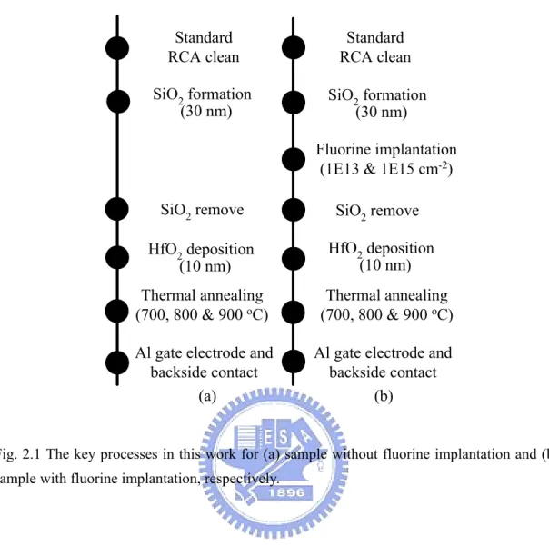
temperatures of 700, 800 and 900℃, respectively. The 300 nm thick Aluminum film was evaporated for top and bottom electrode to form the MOS capacitors by thermal evaporator. The process flow was schematic and summarized in Fig. 2.1.
The electrical properties were analyzed by HP 4285 for capacitance-voltage (C-V) characteristics at 100 kHz, and the effective oxide thickness (EOT) was extracted from the capacitance under the accumulation region without considering the quantum
effect. The current-voltage (I-V) curves were measured by HP 4156C. In addition, the fluorine concentration was measured by secondary ion mass spectroscopy (SIMS). Moreover, the physical thickness was checked by a transmission electron microscopy (TEM) to obtain the dielectric constant. The X-ray Diffraction (XRD) analysis was used to realize the crystallization phenomenon of the HfO2 thin film.
2-1.3 Results and discussion
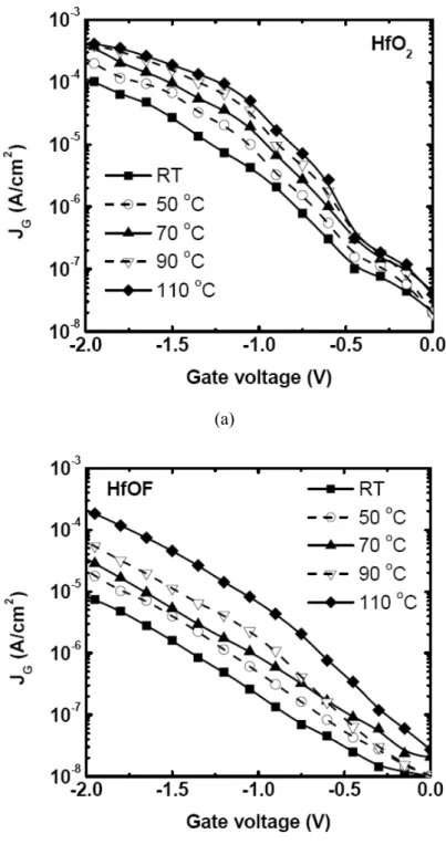
A typical fluorine profile, for the samples with F dose of 1 x 10¹³ /cm2 and 1 x 10¹⁵ /cm2, measured by secondary ion mass spectroscopy (SIMS) was shown in Fig. 3.2. The fluorine concentration was increased with increasing the dosage of fluorine implantation. The transmission electron microscopy (TEM) image of the sample with fluorine incorporation (F dose 1 x 10¹⁵ /cm2) was illustrated in the inset of Fig. 2.2. The physical thickness of the HfO2 film is 4.7 nm and an interfacial layer of 2.9 nm
formed between the HfO2 thin film and the Si-substrate was also observed in this
figure. Besides, the other interfacial layer was formed between the HfO2 thin film and
the Al-gate. The effective dielectric constant derived based on the physical thickness, including the interfacial layers, is about 15. We can also observe that the fluorine atoms were accumulated mainly at the interfacial layer for the sample with F dose of 1 x 10¹⁵ /cm2. Therefore, we suggest that after fluorine implantation, the fluorine atoms would accumulate at the surface of the Si substrate, and then distributed into the bulk of HfO2 thin film after annealing, as shown in Fig. 2.3. The incorporated
fluorine will replace the hydrogen bond and terminate the dangling bond. Figure 2.4 (a) and (b) has shown the X-rays diffraction (XRD) patterns of 50 nm thick HfO2 and
HfOxFy films, respectively. The HfO2 films with fluorine implantation would not be
the fluorine incorporation could restrain the crystallization for HfO2 films with 700oC
PDA treatment. Besides, for the HfO2 films with 800°C PDA, we observed a weak
degree of crystallization; on the other hand, for the as-deposited sample annealed above 800°C, a well crystallized structure with an HfO2 (111) orientation was
observed.
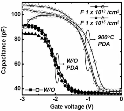
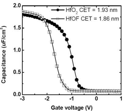
Fig. 2.5 shows the capacitance-voltage (C-V) curves of the HfO2 films with and
without fluorine implantation and 900oC annealing. The large flat band voltage shift of the HfO2 films without annealing was obtained due to the plasma damage induced
by sputtering of the thin films. After 900°C annealing, the flat band voltage would be improved as shown in this figure. This post-deposition RTA process will reduce the flat band voltage and dense the thin film. Furthermore, the C-V distortion of the HfO2
films with only RTA process was observed at the high negative gate bias owing to the crystallization induced leakage current. The high thermal stability in the EOT change was obtained for the fluorine-implanted samples as shown in Fig. 2.6. After high temperature annealing, the EOT of the sample without fluorine implantation was much thicker than the HfO2 films with fluorine implantation. We also observed that
the thermal stability in EOT was significantly improved with increasing the fluorine implantation dosage. The EOT of the sample without fluorine implantation was increased with increasing PDA temperature for about 2.7 Å, whereas the EOT increase was suppressed to less than 0.3 Å for the F-implanted sample (1°1015 cm-2). Fig. 2.7 shows the gate current density versus the gate voltage (J-V) characteristics of all samples with and without 900°C RTA annealing. As we can see, the gate leakage current of the sample without fluorine implantation was much larger than the films with fluorine implantation. Not only the leakage current but also the breakdown voltage was improved for the sample with fluorine incorporation. The characteristics were improved with increasing the fluorine implantation dosage as illustrated in this
figure. In addition, the HfO2 films with fluorine implantation exhibit superior thermal
stability in gate leakage as shown in Fig. 2.8. With the increase of the annealing temperature, the increase of gate leakage current of the fluorine-implanted samples was significantly diminished. This indicated that the fluorine incorporation reduces the defect density at the bulk HfO2 film and the HfO2/IL interface. The thermal
stability of the relationship between gate leakage current density at VG = VFB -1 V and
capacitance equivalent oxide thickness was shown in Fig. 2.9. The gate leakage current for the sample without fluorine implantation was much higher than the sample with fluorine implantation while the EOT is the same for all these three samples with 700°C PDA. Besides this, the gate leakage current of all samples was increased as the PDA temperature increasing. The leakage current of the control sample with high temperature (900°C) PDA was much larger than that of the samples with fluorine implantation as illustrated in this figure. The gate leakage current density of the sample with 1°1015 cm-2 F-implantation, was three orders improved as compared to the control sample with PDA at 900°C. This indicated that the thermal stability was much improved after the fluorine incorporation. The same tendency was shown in the performance of the equivalent oxide thickness (EOT). Even after PDA at 900 °C, low EOT (25.4 Å) was obtained while keeping the leakage current less than 0.1 mA/cm2 for the HfO2 films with SSFI. The superior thermal stability of the F-incorporated
HfO2 gate dielectrics can be explained by the Si-H bond being replaced by Si-F and
strengthened the interface quality of HfO2/Si interface.
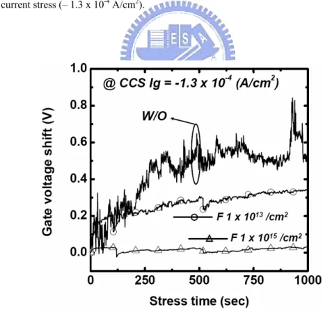
Fig. 2.10 shows the stress induce leakage current (SILC) characteristics of the HfO2 films without post-deposition RTA process. We can find that the gate leakage
current increases with the stress time. This increase of leakage current in the low field region is due to the trap assisted tunneling process, which is analogous to the stress induced leakage current (SILC) in SiO2 [2.14]. Compared to the sample without
fluorine implantation, the HfO2 films with fluorine implantation present small SILC
current, which is due to the defect density being reduced as shown in Fig. 2.11. The gate leakage current of the HfO2 films without post-deposition RTA process increase
under stress was reduced with increasing the dosage of the fluorine implantation as indicated in Fig, 2.11. Therefore, the fluorine incorporation would improve the charge trapping effect in HfO2 gate dielectrics [2.15]. Fig. 2.12 demonstrates the charge
trapping characteristics of these samples without post-deposition RTA process under constant current stress (CCS) at Jg = -1.3 x 10⁻⁴ A/cm2. The hole trapping was observed for all samples as shown in this figure, and was effectively suppressed for the F-incorporated HfO2 gate dielectrics. In addition, the reduced gate voltage shift is
obtained for the increased dosage of the fluorine implantation. This reduction of charge trapping indicates that the characteristics for the HfO2 thin film were improved
after the fluorine implantation at the silicon surface. The physical model of fluorinated HfO2 gate dielectrics was proposed to explain the charge trapping
reduction as shown in Fig. 2.13. Both the electron and hole trappings occurred in the HfO2 thin film under constant voltage stress but located at different side of the HfO2
gate dielectrics. The electron trapping takes place in the HfO2 layer, while the positive
charge (hole) is generated close to the HfO2/Si interface where a lot of defects are
presented [2.16]. We believe that the more defect density at the HfO2/Si interface than
the bulk HfO2 film for the sample without fluorine implantation resulted in the hole
trapping and indicated in Fig. 2.13(a). For the SSFI HfO2 gate dielectrics, the fluorine
atoms will distribute in the interface between the HfO2 film and silicon substrate.
Therefore, the hole trapping was effectively reduced, and then resulted in the less hole trapping observed at the fluorinated HfO2 gate dielectrics as illustrated in Fig. 2.13(b).
In summary, an approach to improve the thermal stability of the HfO2 by
fluorine ion implantation at the silicon surface was proposed and systematic studied. The HfO2 thin film with fluorine implantation was not crystallized and performed
superior thermal stability even after high temperature annealing. This must be owing to the elimination of interface dangling bonds and the bulk traps for the HfO2 films
with pre-deposition fluorine implantation and post-deposition annealing. Besides, the charge trapping characteristics of SSFI HfO2 gate dielectrics was studied and
effectively improved for the samples with SSFI. This fluorinated technology could be used on HfO2 thin films for future ULSI application.
Fig. 2.1 The key processes in this work for (a) sample without fluorine implantation and (b) sample with fluorine implantation, respectively.
Standard RCA clean
Fluorine implantation (1E13 & 1E15 cm-2)
HfO2 deposition (10 nm)
Al gate electrode and backside contact Standard
RCA clean
HfO2 deposition (10 nm)
Al gate electrode and backside contact (a) (b) SiO2 formation (30 nm) SiO2 formation (30 nm) SiO2 remove SiO2 remove Thermal annealing (700, 800 & 900 oC) Thermal annealing (700, 800 & 900 oC)
Fig. 2.2 The SIMS depth profile of MOS with fluorine implantation (dose : 1 x 10¹⁵ /cm2)
structure for fluorine. The peak value for fluorine is located at the interface of HfO2 and
silicon substrate. The inset figure is the TEM of MOS structure with fluorine (dose : 1 x 10¹⁵
/cm2) implantation.
Fig. 2.3 The physical model for the distribution of the fluorine atoms. The fluorine atoms would diffuse into the HfO2 thin film after thermal annealing.
(a)
(b)
Fig. 2.4 The XRD data for (a) as-deposited sample and (b) the samples with fluorine implantation with different PDA temperature, respectively. The sample without fluorine implantation was crystallized after 700℃ PDA.
Fig. 2.5 The C-V curves for all samples. The flat band voltage shift positively after 900℃ annealing.
Fig. 2.6 The thermal stability in EOT for all samples. The EOT increase is much smaller for the sample with fluorine implantation.
Fig. 2.7 The J-V curves (gate leakage current) for all samples. The leakage current was reduced for sample with fluorine implantation, especially in the condition for 900 ℃ annealing.
Fig. 2.8 The gate leakage current density at Vg = -2V for all samples with different annealing temperature. The thermal stability was much improved after fluorine implantation.
Fig. 2.9 The relationship of the thermal stability between the gate leakage current density (at Vg = -2 V) and the capacitance equivalent oxide thickness for all samples with the different annealing temperature.
Fig. 2.10 The stress induce leakage current (SILC) characteristics of the as-deposited and the sample with fluorine implantation under negative current stress (– 1.3 x 10⁻⁴ A/cm2).
Fig. 2.11 The gate leakage current of stress induce leakage current (SILC) for all samples under constant current stress (– 1.3 x 10⁻⁴ A/cm2).
Fig. 2.12 Charge trapping characteristics of the as-deposited and fluorine implanted samples with under constant current stress (– 1.3 x 10⁻⁴ A/cm2).
Fig. 2.13 The physical model of charge trapping mechanism under constant current stress for (a) as-deposited sample, (b) fluorine incorporated sample.
2-2 Current Transport Mechanism of TaN/HfO2/IL/Si Structure with Silicon
Surface Fluorine Implantation (SSFI)
2-2.1 Introduction
High-k gate dielectrics, as an alternative to conventional SiO2 gate oxide, are
widely investigated for their capability to reduce gate-leakage current for the same electrical capacitance [2.17]–[2.19]. Among all high-k gate materials, hafnium-based dielectrics are considered the most promising candidates, or at least the most studied, due to their excellent thermal stability, wide bandgap, and high dielectric constant [2.20]-[2.22]. Nevertheless, the metal-gate electrode has also attracted attention as a solution to the polydepletion effect that appears under gate inversion conditions in poly-Si gates, and the incompatibility between some high-k materials and poly-Si [2.23]. As a result, metal gate/high-k stacks have been heavily explored in recent years [2.23]-[2.26].
However, HfO2 gate dielectrics with fluorine incorporation could also exhibit
better dielectric performance and reliability [2.27]-[2.31]. F incorporation into HfSiON dielectric has been shown to be highly effective in lowering Vth and
improving NBTI in pFET, and the drive current could be aggressively increased [2.27]. F is believed to form stronger Hf-F and Si-F bonds than Hf-H and Si-H bonds, which improves the reliability of HfO2/SiO2 [2.28]. Recently, we have also
documented several studies of ultra-thin fluorinated HfO2 gate dielectrics. First, the
thermal stability of HfO2 gate dielectrics can be much improved by fluorine ion
implantation on the silicon surface [2.32]. Second, the interfacial layer (between HfO2
film and Si-sub.) formation can be effectively suppressed by pre-CF4 plasma
treatment [2.33]. Third, the charge trapping phenomenon can be largely eliminated for the HfO2 gate dielectrics fluorinated by postdeposition CF4 plasma treatment [2.34].
Although several recent studies have investigated fluorinated HfO2 gate dielectrics
[2.27]-[2.34], its carrier transport mechanisms have not been well investigated. Only a few studies have demonstrated the carrier transport and tunneling mechanisms of conventional HfO2 gate dielectrics [2.35]-[2.37], and none have explored fluorinated
HfO2 gate dielectrics. Electron transport in high-k gate dielectrics will instead be
governed by a trap-assisted mechanism, such as Frenkel–Poole conduction or hopping conduction, due to the charge trapping phenomenon. The band diagram of the metal/HfO2/Si capacitor has been investigated, though without consideration of the
interfacial layer [2.35]. However, the interfacial layer is a critical issue for high-k gate dielectrics, and deserves in-depth discussion.
In this section, we investigate the carrier transportation mechanism in devices integrating both HfO2 gate dielectrics with and without fluorine incorporation and a
metal gate (TaN). We present new, accurate characterizations of TaN/as-deposited and fluorinated HfO2/Si capacitors, including Frenkel-Poole conduction and
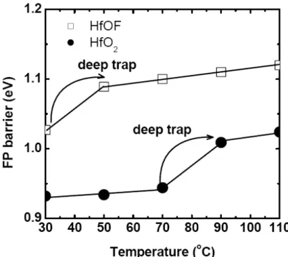
Fowler-Nordheim tunneling, under both gate and substrate injection modes. The strong temperature dependence of the gate leakage current suggests that the current tunneling mechanism is Frenkel-Poole conduction for both as-deposited and fluorinated HfO2 gate dielectrics. The effective extracted trapping level of fluorinated
HfO2 gate dielectrics is thus larger than the as-deposited one. We also report the
Fowler–Nordheim tunneling characteristics at 77 K, from which we can deduce the energy band diagrams for TaN/HfO2/IL/Si and TaN/HfOF/(IL+F)/Si structures, as
well as their current transport mechanisms.
2-2.2 Experiment
wafers. First, standard RCA cleaning was performed on all samples. Then, 30 nm screen oxide films were grown in order to prevent implantation damage. Fluorine ions were implanted through the 30 nm screen oxide films at a low energy of 25 keV, with different dosages ranging from 1×10¹³/cm2 to 1×10¹⁵/cm2, designated F 1E13, F 1E14, and F 1E15 (without F implantation, denoted as as-dep.), respectively. Then, annealing in an N2 ambient at 850°C for 30 minutes was performed, to remove any
implant-induced damage. At that time, the fluorine atoms diffused into the silicon surface.
Before HfO2 thin film deposition, the 30 nm screen oxide was removed by wet HF
solution. Then, an HfO2 thin film was then deposited on a HF-last Si surface by an
electron beam evaporation system. For HfO2 thin film crystallization study, some
samples were annealed by rapid thermal annealing in the N2 ambient for 30 seconds at
600°C. The HfO2 thin film was crystallized after the 600°C rapid thermal annealing,
as approved in XRD analysis (not shown here). Metal gate (TaN) film of 50 nm was deposited by reactive RF sputter for all samples. Thereafter, a 300 nm thick Al film was deposited on the TaN film by thermal evaporator. The gate of the capacitor was defined lithographically and etched. Finally, a 300 nm thick Al film was also deposited on the backside of the wafer to form the ohmic contact.
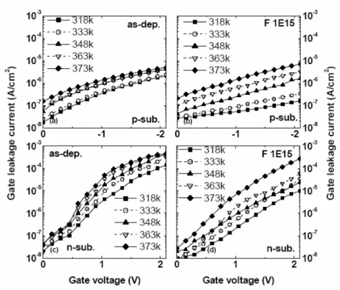
The electrical properties were analyzed by an HP 4285 for capacitance-voltage (C-V) characteristics at 100 kHz, and the capacitance effective thickness (CET) was extracted from the capacitance under the accumulation region without considering the quantum effects. The current-voltage (I-V) curves were measured by a Keithly 4200. Further, the I-V characteristics were measured at elevated temperature (318-373 K) and low temperature (77 K), in order to study the current transportation and band diagram of the MOS capacitor, respectively. Moreover, the physical thickness was checked by transmission electron microscopy (TEM) to obtain the dielectric constant
of HfO2 thin film.
2-2.3 Results and discussion
Take-off angles of 60o and 90° were used to measure the XPS spectra of surface and bulk HfO2 thin films with fluorine incorporation (Figure 2.14). In Figure 2.14, for
all samples except the as-deposited sample, a distinct F 1s peak at 687 eV can be observed. The silicon surface fluorine implantation processes are apparently introducing fluorine atoms into the dielectrics to form the HfOF gate dielectrics. However, the fluorine intensity was larger for the TOA = 90o than TOA = 60o, indicating that less fluorine would distribute in bulk HfO2 gate dielectrics. Figure 2.15
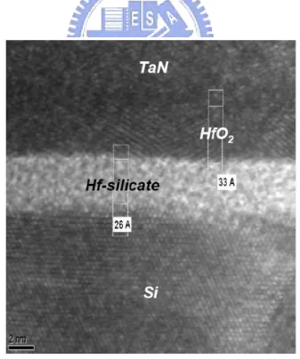
shows the TEM image of the TaN/HfO2/IL/Si structure with fluorine incorporation
(1×10¹⁵/cm2) and 600°C postdeposition annealing (PDA). The great quality of the HfO2 thin film was demonstrated in this study, as Figure 2.15 shows. As discussed
before, PVD deposited HfO2 thin films tend to have interfacial layers (IL) at the
HfO2/Si interfaces as shown in the TEM images. In addition, the composition of the
interfacial layer is believed to be hafnium silicate, because the estimated dielectric constant of the interfacial layer is higher than that of the SiO2. Furthermore, the
thickness of HfO2 and Hf-silicate were about 3.3 and 2.6 nm, respectively. As a result,
the k value of the HfOF (with Hf-silicate) thin film was about 14. In this work, the carrier transportation mechanism of both as-deposited and fluorinated HfO2 gate
dielectrics was investigated, while taking into account the Hf-silicate interfacial layer. Figure 2.16 shows the gate current density versus the gate voltage (J-V) characteristics of all samples with and without 600°C RTA annealing under (a) gate injection and (b) substrate injection modes, respectively. As we can see, the gate leakage current of the sample without fluorine implantation was much larger than that