國 立 交 通 大 學
電子工程學系 電子研究所
碩 士 論 文
原子層沉積氧化鋁閘極介電層之砷化鎵通道
元件電性研究
A study on the electrical properties of GaAs channel devices
with atomic-layer-deposited Al
2O
3gate dielectric
研 究 生 : 何 宗 霖
指
導
教
授 : 簡 昭 欣 教授
原子層沉積氧化鋁閘極介電層之砷化鎵通道元件電性研究
A study on the electrical properties of GaAs channel devices
with atomic-layer-deposited Al
2O
3gate dielectric
研 究 生:何宗霖 Student : Tsung-Lin He
指導教授:簡昭欣 教授 Advisor : Dr .Chao-Hsin Chien
國 立 交 通 大 學
電子工程學系 電子研究所碩士班
碩 士 論 文
A Thesis
Submitted to Department of Electronics Engineering
& Institute of Electronics
College of Electrical and Computer Engineering
National Chiao Tung University
In Partial Fulfillment of the Requirements
For the Degree of Master
In
Electronics Engineering
October 2010
Hsinchu, Taiwan, Republic of China
i
原子層沉積氧化鋁閘極介電層之砷化鎵通道
元件電性研究
學生:何宗霖 指導教授
:簡昭欣 教授
國 立 交 通 大 學
電子工程學系 電子研究所 碩士班
摘要
在此篇文獻中,我們已經最佳化表面處理使得砷化鎵的表面費米能階可成功到達 反轉區,也將砷化鎵能隙中間的 Dit值降低至 2E12cm -2 V-1 。首先,我們先探討利用原子層 沉積氧化鋁做為閘極氧化層的電容電性,使用 Berlund 積分公式求出半導體表面費米能 階與閘極電壓關係,並且比較不同 Dit在砷化鎵能隙中分佈的萃取方式。其次,我們探 討在沉積氧化鋁之前,利用三甲基鋁,還原基板表面的氧化物,其對砷化鎵電容特性的 影響。雖然在電容的電性以及 XPS 分析上沒有發現明顯的改善,但是經過 TEM 照片的輔 助,計算出閘極氧化層的介電值與等效氧化層厚度有明顯的改進。接著,我們探討不同 表面晶向(100)與(111)A 的基板的電容特性。發現利用基板晶向為(111)A 的電容特性具 有很大的改進,可以使表面費米能階成功到達反轉區,也將砷化鎵能隙中間的 Dit值降 低,我們推測改善是源自於基板表面結構不同所致。針對電容研究的情形,我們利用已 經最佳化過後的表面處理去製作出砷化鎵場效應電晶體。ii 最後我們成功在半絕緣的基板上製作出原子層沉積氧化鋁高介電層之增強式砷化 鎵 N 型場效電晶體。砷化鎵場效電晶體( 寬度/長度 = 100 μm/50 μm )的載子遷移率峰值 為 15 cm2 V-1s-1,而電晶體( 寬度/長度 = 100 μm/5 μm )的電流開關比為 4.12E3。雖然成 功製作出電晶體,不過元件特性尚未預期的好,我們推測是由於電晶體的源極與汲極的 活化步驟的條件沒掌控好所導致。此外,我們也成功製作出通道為砷化銦鎵而源極與汲 極為磊晶鍺異質接面的金半場效電晶體,並探討其元件特性。
iii
A study on the electrical properties of GaAs channel devices
with atomic-layer-deposited Al
2O
3gate dielectric
Student:Tsung-Lin He Advisor : Dr .Chao-Hsin Chien
Department of Electronics Engineering and Institute of Electronics
National Chiao Tung University
Abstract
In this thesis, we demonstrated that the Fermi level (EF) of GaAs on the surface could be adjusted to the level of the inversion mode via optimizing the surface treatment. With the optimized treatment, the interface state density (Dit) in the middle of energy bandgap of GaAs could be significantly eliminated to a value of 2E12cm-2V-1. At first, we studied the electrical characteristics on GaAs MOS capacitor with Al2O3 gate dielectric formed by atomic-layer-deposition (ALD). We not only utilized Berglund’s integration to obtain the relation between surface potential and gate voltage but also compared the Dit distribution within energy bandgap by the different extraction methods. Next, we studied the reduction of native oxides on GaAs substrates by trimethylaluminum (TMA) pretreatment before ALD of Al2O3 and examined the impact of the electrical characteristics on GaAs MOS capacitors. Although we did not observe anything different on electrical characteristics and XPS analysis,
iv
we found the improvement in the value of k and effective oxide thickness after calculation with the TEM image. Then, we studied the electrical characteristics on GaAs MOS capacitors with the different surface orientation of substrates. There was improvement on GaAs MOS capacitors with (111)A surface orientation. The EF of surface on GaAs could reach inversion region and the value of Dit in the middle of energy bandgap was decreased. We presumed that improvement was caused by the different structure of surface on substrate.
Finally, we fabricated E-mode GaAs n-MOSFET on semi-insulator substrate. The electronic mobility we extracted was 15 cm2V-1S-1 and the on/off ratio was 4.12E3; the lower mobility and poor on/off ratio were due to the unsuccessful S/D activation. In addition, we also fabricated InGaAs channel MESFET with Ge S/D and studied electrical characteristics.
v
誌謝
時光飛逝,碩士班短短兩年收穫良多。首先,最重要感謝的是我的指導教授簡昭 欣教授。提供我,在實驗上有充足的資源能夠盡情的嘗試;教導我,在研究上用嚴謹的 態度面對問題的探討;叮囑我,在個性上須謙卑的角度改善自身的缺點。可以作為這位 好老師的研究生,實在是上輩子修來的福氣。 其次是要感謝兆欽學長,學長對研究的熱忱,對知識的追求,積極的態度是令我 們後輩做學弟所敬佩及學習。還有宗佑學長,客氣魔人,感謝學長這兩年來的指導,不 論是在實驗的操作以及研究的理論,跟學長討論過後受益許多,也感謝學長在實驗及量 測上的幫助才能夠讓我完成我的碩士論文,非常感謝。當然也不能忘記常常一起在無塵 室做實驗和在摩斯漢堡吃飯的浩宇學長,學長對學弟的照顧我會謹記在心。實驗室畢業 的學長,欣哲,當初介紹我進入這個大家庭,你的牽引使我的兩年生活多采多姿;胖哥, 搞笑又有趣的語言能力真是令人難以忘懷。當然也不能夠忘記小豬、大鳥、陞哥,感謝 你們不辭辛勞教學機台的操作和實驗的小撇步,我的實驗才能夠順順利利。另外還有很 多很棒的學長們,豪育學長、明瑞學長、志彥學長,在 meeting 的建議讓我在報告上更 有心得。 國永跟禎晏,我們共同度過碩一修課的日子,也一起經歷碩二實驗的日子;忙著 上課交報告期中期末考,忙著研究學機台趕實驗進度。雖然你們先走一步,不過還是很 感謝這兩年的陪伴。 實驗室往後的戰力,家豪學長,恭喜快要當爸爸了,預祝學長明年雙喜臨門。宇 彥學長、京璋學長還有我們偉大的吳博學長,未來有機組就靠你們打拼。尤其是吳博學 長說好的十篇,大家都等著雞犬升天。政庭學長,還記得我們常常搭乘小巴士、在清大 夜市踩雷、喝著有茶氏,這一兩年下來時在是太多回憶了。宗元學長還有信淵學長,有 實力派的你們加入,實驗室陣容越來越堅強了。哲偉,想當初三年前我們還在同一間教 室上課,如今你卻坐在我隔壁,我們還是一樣無所不聊,恭喜你攻讀博士班,希望日後vi 你的實驗順利。Roger、Camber、Rego 以及姿慧剩下一年好好加油,實驗室也要靠你們 極力貢獻了,燃燒你們的小宇宙吧。 接些來得也感謝我的大學學長,峻丞及鈞任,說是貴人也不為所過。感謝你們從 大一就開始指導我,如何準備學校的課業、研究所的考試、處理生活的問題,還記得你 們從大學畢業之後,也會不時的回彰化找我聊天聚餐,每每跟你們聊過天之後,深深覺 得自己又上了一課,感謝你們的栽培與提拔,祝福你們在工作上都能順心。大學同學們, 富蓁,謝謝妳常常帶著點心來探監;嘉憲、茹嬅、國榮、徐燁、阿舍、空空、家祥、種 子、童童、鍾媽,能夠在異鄉與你們聚餐實在是很令人開心的事。大學學弟們,佳信、 野人、新鈞、同偉,恭喜你們進入交大電子這大家庭,你們的未來一定會比我更優秀; 小沙、聖璁、光華,你們在交大電物一定可以開拓新的視野。 再來要感謝我的朋友,莛潔,謝謝妳在我開始展開新生活時不辭辛勞地陪我找房 子,帶我認識新竹這的環境;還有侑妘,與妳用 MSN 聊天常讓我緊張的生活舒壓不少; 當然不能忘記小古,這兩年來的陪伴,讓我碩士的求學過程充滿了意想不到、除了知識 以外的收穫;文君,妳的創作給了我很大的滋養及鼓舞。當然不能缺少園區的朋友們, 阿名、小肥、菜菜、大可、哈哈、阿凱、明峰,不管是假日的出遊還是週末的小聚都充 實著我碩士的回憶。感謝我的朋友們的陪伴,認識你們真好。 最後,一定不能缺少的就是我的家人。辛苦老媽,萬分感謝您一直以來的支持還 有鼓勵,從小就扶養我栽培我督促我,才使我有至今的碩士學位,謝謝您;辛苦老哥, 在我異鄉求學的日子都是您照顧老媽,感謝您的付出;老爸,無論你在哪在做什麼,加 油。在此希望我的家人還有我的朋友每天都能開開心心、身體健康,並且將這份成就與 我愛的家人和朋友分享。 何宗霖 於 新竹國立交通大學 2010/10/12
vii
Contents
Abstract (Chinese) --- i
Abstract (English) --- iii
Acknowledgments --- v Contents --- vii Table Captions --- x Figure Captions --- xi
Chapter 1
Introduction
1.1 General Background --- 1 1.2 Motivation --- 21.3 Organization of This Thesis --- 3
References --- 4
Chapter 2
Electrical characteristics of GaAs MOS capacitor
with Al
2O
3gate dielectric
2.1 Introduction --- 82.2 Sample Preparation --- 11
viii
2.3.1 Multi-Frequency C-V of GaAs MOS Capacitor --- 12
2.3.2 Conductance Method Application of GaAs MOS Capacitor --- 13
2.3.3 Comparison of Dit Extraction --- 13
2.1 Summary --- 14
References --- 15
Chapter 3
Optimization of Al
2O
3/GaAs interface with MOS capacitor
3.1 Introduction --- 243.2 Experimental Procedures --- 26
3.3 Results and Discussion --- 28
3.3.1 TMA Effect --- 28
3.3.2 PDA Effect --- 29
3.3.3 Surface Orientation Effect --- 30
3.4 Summary --- 31
References --- 33
Chapter 4
Fabrications of GaAs MOSFET and InGaAs MESFET
4.1 Introduction --- 474.2 Experimental Procedures --- 49
4.2.1 Device Structure ( MESFET ) --- 49
ix
4.2.3 Device Structure ( MOSFET ) --- 50
4.3 Results and Discussion --- 51
4.3.1 Electrical Characteristics of InGaAs MESFET --- 51
4.3.2 Electrical Characteristics of Ge-S/D InGaAs MESFET --- 52
4.3.3 Electrical Characteristics of E-mode GaAs n-MOSFET --- 53
4.4 Summary --- 54
References --- 55
Chapter 5
Conclusion and Suggestions
5.1 Conclusion --- 695.2 Suggestions --- 70
x
Table Captions
Chapter 3
Tab. 3.1 The experimental condition of Si-doped ( p-type, ~ 5×1017 cm-3 ) GaAs MOS capacitors were in this study. --- 27
Chapter 3
Tab. 4.1 The resistance parameters by transfer length method ( TLM ) test structure of InGaAs MESFET. --- 63
xi
Figure Captions
Chapter 1
Fig. 1.1 Transistor scaling and research roadmap demonstrated by R. Chau, Intel Corp.
--- 6
Fig. 1.2 One of the several possible future high-performance CMOS architecture by D. Lin, IMEC. --- 7
Chapter 2
Fig. 2.1 Equivalent circuits for conductance measurements; (a) MOS capacitor, (b) simplified circuit, (c) measured circuit, (d) including series rs resistance and tunnel conductance Gt. --- 17 Fig. 2.2 Characteristic emission frequencies of trapped charge carriers in GaAs at the
different temperatures. --- 17
Fig. 2.3 The structure and process flow of Al/Al2O3/p-GaAs (100)/TiPtAu MOS capacitor.
--- 18
Fig. 2.4 Multi-frequency C-V curve of Al/Al2O3/p-GaAs (100)/TiPtAu MOS capacitor at (a) 25℃, (b) 125℃measurement condition. --- 19
Fig. 2.5 Quasi-static C-V curve of Al/Al2O3/p-GaAs (100)/TiPtAu MOS capacitor. --- 20 Fig. 2.6 Surface potential versus gate voltage of Al/Al2O3/p-GaAs (100)/TiPtAu MOS
capacitor. --- 20
Fig. 2.7 Dit distribution by high-low frequency method of Al/Al2O3/p-GaAs (100)/TiPtAu MOS capacitor. --- 21
xii
Fig. 2.8 Series resistance extraction of Al/Al2O3/p-GaAs (100)/TiPtAu MOS capacitor.
--- 21
Fig. 2.9 Gp/ as a function of frequency (a) and (b) at 25℃ measurement condition; (c) and (d) at 125℃ measurement condition. --- 22
Fig. 2.10 Dit distribution by conductance methods of Al/Al2O3/p-GaAs (100)/TiPtAu MOS capacitor. --- 23
Fig. 2.11 Comparison of Dit extractions by high-low frequency method and conductance methods of Al/Al2O3/p-GaAs (100)/TiPtAu MOS capacitor. --- 23
Chapter 3
Fig. 3.1 Atomic layer deposition ( ALD )-Al2O3 mechanism and chemical reaction.
--- 35
Fig. 3.2 The structure and process flow of Al/Al2O3/GaAs/TiPtAu MOS capacitor.
--- 36
Fig. 3.3 Frequency-dependent C-V curves of Al/Al2O3/p(100)-GaAs/TiPtAu MOS capacitors. (a)without, (b)with TMA pretreatment. --- 23
Fig. 3.4 Comparison of surface potential fluctuation of TMA effect of Al/Al2O3/p-GaAs (100)/TiPtAu MOS capacitors. --- 38
Fig. 3.5 Comparison of Dit distribution of TMA effect of Al/Al2O3/p-GaAs (100)/TiPtAu MOS capacitors. --- 38
Fig. 3.6 As 2p3/2 XPS spectra of Al2O3/GaAs interface subjected to with and without TMA pulse. --- 39
Fig. 3.7 The cross-section of TEM image of Al/Al2O3/GaAs : (a) without TMA pretreatment; (b) with TMA pretreatment. --- 40
xiii
Fig. 3.8 Frequency-dependent C-V curves of Al/Al2O3/p(100)-GaAs/TiPtAu MOS capacitors at 25℃ and 125℃measurement condition with TMA pretreatment, (a) and (c) as-deposited; (b) and (d) withPDA. --- 41
Fig. 3.9 Comparison of surface potential fluctuation of Al/Al2O3/p-GaAs (100)/TiPtAu MOS capacitors with and without PDA. --- 42
Fig. 3.10 Comparison of Dit distributions of Al/Al2O3/p-GaAs (100)/TiPtAu MOS capacitors with and without PDA. --- 42
Fig. 3.11 Comparison of Dit distribution of Al/Al2O3/p-GaAs (100)/TiPtAu MOS capacitors with and without PDA. --- 43
Fig. 3.12 C-V curves of Al/Al2O3/p-GaAs/TiPtAu MOS capacitors (a) (100), (b) (111)A surface orientation. --- 44
Fig. 3.13 Comparison of surface potential fluctuation of surface orientation effect of Al/ Al2O3/p-GaAs/TiPtAu MOS capacitors. --- 45 Fig. 3.14 Comparison of Dit distribution of surface orientation effect of Al/Al2O3/p-GaAs/
TiPtAu MOS capacitors. --- 45
Fig. 3.15 Empirical model of GaAs (111)A and (100) surface. The minimum Dit and U-shape curvature depend on processing conditions, while the location of E0 remains constant for each semiconductor with the same crystal face. --- 46
Chapter 4
Fig. 4.1 The scheme of MBE InGaAs and the fabricated InGaAs MESFET process flow.
--- 58
Fig. 4.2 The scheme and process flow of MESFET with Ge-S/D on InGaAs structure. -- 59
Fig. 4.3 The TEM image of Ge film which was grown by UHV/CVD system on semi-insulator GaAs substrate. --- 60
xiv
Fig. 4.4 The scheme and process flow of E-mode GaAs n-MOSFET on semi-insulator substrate. --- 61
Fig. 4.5 Source to drain current with the different recess gate etching depth of GaAs MESFET. --- 62
Fig. 4.6 Total resistance with the different recess gate etching depth of InGaAs MESFET and the inset is TLM test structure ( L=50μm Z=100μm ). --- 62
Fig. 4.7 Transfer characteristic for InGaAs MESFET with 8 μm gate length. The best Ion/Ioff( @ VDS = 1.5 V ) is about . --- 63 Fig. 4.8 Output characteristic ( ID-VD ) with different gate bias for InGaAs MESFET with
8 μm gate length. --- 64
Fig. 4.9 Total resistance of InGaAs MESFET with Ge-S/D and the inset is TLM test structure ( L=50μm Z=100μm ). --- 64
Fig. 4.10 Transfer characteristic for InGaAs MESFET with Ge-S/D with 3 μm gate length. The best Ion/Ioff ( @ VDS = 1 V ) is about . --- 65 Fig. 4.11 Output characteristic ( ID-VD ) for for InGaAs MESFET with Ge-S/D with 3 μm
gate length. --- 65
Fig. 4.12 Transfer characteristic of E-mode GaAs n-MOSFET with 5μm gate length. Ion/Ioff( @ VDS=2V ) is about . --- 66 Fig. 4.13 Trans-characteristic ( Gm ) versus gate bias ( VG ) of E-mode GaAs n-MOSFET
with 5μm gate length. The peak Gm is 0.35 nS/μm. --- 66 Fig. 4.14 Output characteristic ( ID-VD ) for E-mode GaAs n-MOSFET with 5μm gate
length. The maximum drain current is 9 nA/μm. --- 67
Fig. 4.15 The gate-to-channel capacitance and inversion charge density of E-mode GaAs n-MOSFET with 5μm gate length. --- 67
1
Chapter 1
Introduction
1.1 General Background
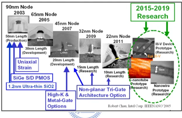
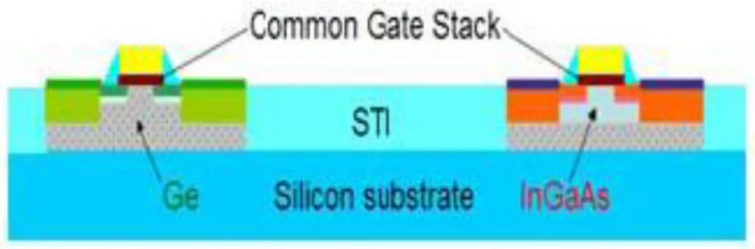
Silicon-based complementary metal-oxide-semiconductor (CMOS) devices with traditional structures are approaching fundamental physical limits. R. Chau, Intel Corporation, had even demonstrated the scaling roadmap of the future in the progress of the Si metal-oxide-semiconductor field-effect transistor (MOSFET), as shown in Fig. 1.1. D. Lin, Interuniversity Microelectronics Center (IMEC vzw), reported that one of the several possible future high-performance CMOS architecture [1], as the scheme presented in Fig. 1.2. Because of the feature electronic products demand, CMOS devices is required not only high speed and high performance but also less power consumption. For the above requirements, novel device structures and materials must be investigated.
The advantage of Ⅲ-Ⅴ MOSFET over its Si counterpart has long been recognized because the electron mobility in Ⅲ-Ⅴ compound material is five or more times higher than that in Si. Therefore, Ⅲ-Ⅴ MOSFET have application in high-speed electronic devices, like microwave and digital, and its technology promises the advantages of low-power consumption and circuit simplicity.
Silicon-based technology with its devices of 32 nm gate length in production or the smaller in research and development, and with SiO2 gate oxide thickness close to quantum
2
tunneling limit of 1.0 nm, has called for alternative high-k gate dielectrics. However, Coulomb scattering from charge trapping and the phonon issue related to high-k gate dielectric have resulted the degradation in channel mobility. The choices of applicable to gate dielectric on Ⅲ-Ⅴ compound semiconductor will be required the gate oxide does not react with the semiconductor, and the band offset of the gate oxide on the semiconductor substrate is requested to have over 1eV [2].
1.2 Motivation
Ⅲ-Ⅴ compound semiconductors have the advantages which high electron mobility, high breakdown field, low power consumption and rich band gap engineering [3-5]. Thus they are expected to out-perform silicon-based CMOS applications such as high-speed and low-power consumption devices. GaAs is of great importance for scientific understanding of Ⅲ-Ⅴ interfaces and GaAs MOS devices can be used as a sensitive test bed for all dielectric techniques. The treatment or passivation techniques developed on GaAs can naturally be applied to InGaAs or other Ⅲ-Ⅴ compound semiconductors [6].
The major challenge in developing Ⅲ-Ⅴ devices is large interface states density ( Dit ) associated with dielectric/Ⅲ-Ⅴ interface reduces the free carrier density available for transport and can lower the effective channel mobility. In the past few years, for the studies of the dielectric/Ⅲ-Ⅴ interface, especially the (In)GaAs substrate, the several studies have been devoted in intensively searching the high interface quality insulators and efficient passivation methods. Except for SiO2 and Si3N4, (Gd,Ga)2O3 [7] and atomic-layer-deposited (ALD) Al2O3 [8], HfO2 [9] high-k dielectrics are of particular interest; meanwhile, the sulfur chemical treatment[10], and Si and Ge [11] as the interfacial passivation layers are currently active approaches to protect the surface of III-V semiconductors prior to the dielectric deposition.
3
1.3 Organization of The Thesis
In Chapter 2, we exhibited the common electrical characteristics of MOS capacitors on GaAs substrate and calculated surface potential fluctuation. We also introduced the conductance methods to extract Dit distributions within energy bandgap to compare high-low frequency method.
In Chapter 3, we studied the reduction of native oxides on GaAs substrates before ALD of Al2O3. After trimethylaluminum (TMA) pluses, it is to suppress native oxides on GaAs surface. Subsequently, we deposited ALD-Al2O3 as gate dielectric to fabricate MOS capacitors and examined the impact of interface quality on the electrical characteristics; the capacitance-voltage (C−V) characteristics were studied. Besides, we also investigated the electrical properties on the different surface orientation of GaAs substrates. Two different GaAs substrates, p-type (111)A and p-type (100), were also fabricated MOS capacitors and studied the impact of the different surface orientation on the electrical characteristics.
In Chapter 4, we utilized the results in optimization of Al2O3/GaAs interface to fabricate the enhance-mode GaAs n-MOSFET on semi-insulating GaAs substrate and also fabricated MESFET on InGaAs structures grown by molecular beam epitaxy (MBE). We discussed their Id-Vg and Id-Vd electrical characteristics and determined the electronic mobility, source/drain resistance.
In Chapter 5, finally, we summarized the experimental results in the thesis and gave the conclusion and suggestions for future work.
4
Reference
[1] D. Lin, G. Brammertz, S. Sioncke, C. Fleischmann, A. Delabie, K. Martens, H. Bender, T. Conard, W. H. Tseng, J. C. Lin, W. E. Wang, K. Temst, A. Vatomme, J. Mitard, M. Caymax, M. Meuris, M. Heyns, T. Hoffmann, “Enabling the high-performance InGaAs/Ge CMOS: a common gate stack solution,” Tech. Dig. Int. Electron Devices
Meet., p. 327, 2009.
[2] J. Robertsona, B. Falabretti, “Band offsets of high K gate oxides on III-V semiconductor,”
J. Appl. Phys., vol. 100, p. 014111, 2006.
[3] K. Iiyama, Y. Kita, Y. Ohta, M. Nasuno, S. Takamiya, K. Higashimine, and N. Ohtsuka,
IEEE Trans. Electron Devices, vol. 49, p. 1856, 2002.
[4] J. K. Yang, M. G. Kang, and H. H. Park, J. Appl. Phys. vol. 96, p. 4811, 2004. [5] P. D. Ye, G. D. Wilk, J. Kwo, B. Yang, H. J. L. Gossmann, M. Frei, S. N. G. Chu, J.
P. Mannaerts, M. Sergent, M. Hong, K. K. Ng, and J. Bude, IEEE Electron Device Lett., vol. 24, p. 209, 2003.
[6] M. Xu, Y. Q. Wu, O. Koybasi, T. Shen, and P. D. Ye, “Metal-oxide-semiconductor field-effect transistors on GaAs (111)A surface with atomic-layer-deposited Al2O3 as gate dielectrics,” Appl. Phys. Lett., vol. 94, p. 212104, 2009.
[7] B. Yang, P. D. Ye, J. Kwo, M. R. Frei, H. J. L. Gossnann, J. P. Mannaerts, M. Sergent , M. Hong, K. Ng, and J. Bude, J. Cryst. Growth, vol. 251, p. 837, 2003.
[8] H.-L. Lu, L. Sun, S.-J. Ding, M. Xu, D. W. Zhang, and L.-K. Wang, “Characterization of atomic-layer-deposited Al2O3/GaAs interface improved by NH3 plasma pretreatment,”
Appl. Phys. Lett., vol. 89, p. 152910, 2006.
[9] M. Zhu, C.-H. Tung, and Y.-C. Yeo, “Aluminum oxynitride interfacial passivation layer for high-permittivity gate dielectric stack on gallium arsenide,” Appl. Phys. Lett. vol. 89,
5 p. 202903, 2006.
[10] M.-K. Lee, C.-F. Yen, J.-J. Huang, and S.-H. Lin, “Electrical characteristics of postmetallization-annealed MOCVD-TiO2 films on ammonium sulfide-treated GaAs,”
J. Electrochem. Soc., vol. 153, p. F266, 2006.
[11] H.-S. Kim, I. Ok. M. Zhang, T. Lee, F. Zhu, L. Yu, and J. C. Lee, “Metal gate-HfO2 metal-oxide-semiconductor capacitors on n-GaAs substrate with silicon/germanium interfacial passivation layers,” Appl. Phys. Lett., vol. 89, p. 222903, 2006.
6
7
Fig. 1.2 One of the several possible future high-performance CMOS architecture by D. Lin, IMEC.
8
Chapter 2
Electrical characteristics of GaAs
MOS capacitor with Al
2
O
3
gate
dielectric
2.1. Introduction
Electrical characteristics, such that capacitance-voltage (C-V) and conductance-voltage characteristics (G-V), are regularly used in research and development to understand important parameters of metal-oxide-semiconductor (MOS) capacitor which are like the flatband voltage (VFB), fixed charge (Qf), effective oxide thickness (EOT) and the quality of dielectric/Ⅲ-Ⅴ interface. The C-V and G-V characteristics are the methods of choice to extensively study the interfacial characteristics because of the inherent sensitivity of the electrical measurements and the ease-of-use of the involved methods.
Interfacial characteristic is a crucial challenge for realizing Ⅲ-Ⅴ MOS capacitor. Therefore, it is essential that the quality of interface is evaluated correctly. For example, poor interfacial quality can cause major distortions of the electrical characteristics and result in extensive misconstruction in the interface states density (Dit) or other perfunctory parameters extracted from these measurements. The energy bandgap of III-V materials also affect the conductance characteristics in several ways that do not have to be considered in Si-based devices. The correct interpretation of the used electrical characteristics therefore becomes of
9 paramount importance in III-V technology.
Thorough understanding of the electrical characteristics will give the proper extraction of the MOS capacitor parameters and of the Dit distribution within the energy bandgap. In this chapter, the understanding of the behavior of GaAs MOS capacitor with the Dit contribution is provided based on firmly established Si/SiO2 MOS capacitor theory [1-4].
The conductance method, proposed by Nicollian Goetzberger in 1967, is one of the most sensitive methods to determine Dit [3]. Dit of 109 cm-2eV-1 and lower can be measured. It is also the most complete method, because it yields Dit in the depletion and weak inversion portion of the bandgap, the capture cross-sections for majority carriers, and information about surface potential fluctuation. The technique is based on measuring the equivalent parallel conductance Gp of an MOS capacitor as a function of bias voltage and frequency. The conductance, representing the loss mechanism due to interface traps capture and emission of carriers, is a measure of the interface trap density.
Fig.2.1(a) illustrates the simplified equivalent circuit of MOS capacitor appropriate for
the conductance method. It consists of the oxide capacitance Cox, the semiconductor capacitance Cs, and the interface state capacitance Cit. The capture-emission of carriers by Dit is a losing process, represented by the resistance Rit. It is convenient to replace the circuit of
Fig. 2.1(a) by Fig. 2.1(b), where Cp and Gp are given by Cp Cs
Cit
1 it 2 2.1
Gp q itDit
1 it 2 2.2
where Cit = q2Dit and it = RitCit, the characteristic emission frequencies of trapped charge carriers, given by
it th PNAexp q s kT 1
2.3 The equations are for interface state with a single energy level in the energy bandgap.
10
Interface state at the dielectric/substrate interface, however, are continuously distributed in energy throughout the energy bandgap. Capture and emission occurs primarily by interface state located within a few kT/q nearby the Fermi level, leading to a time constant dispersion and giving the normalized conductance as
Gp qDit
2 itln 1 it
2 2.4
The conductance is measured as a function of the frequency and ploted as Gp/ versus . Gp/ has a maximum at and at that maximum D it = 2.5Gp/q . Hence we could determine Dit from the Gp/ versus and determine from at the peak conductance
location on the -axis.
An approximate expression giving the interface state density in term of the measured maximum conductance is Dit 2.5 q Gp max 2.5
Capacitance meters generally assume the device to consist of the parallel Cm-Gm combination in Fig. 2.1(c). A circuit comparison of Fig. 2.1(b) to Fig. 2.1(c) gives Gp/ in term of the measured capacitance Cm, the oxide capacitance, and the measured conductance Gm as
Gp
GmCox
2
Gm2 2 Cox Cm 2
2.6 In the addition, the device has series resistance which has so far been neglected. Series resistance is a common parasitic affecting C-V and G-V measurement of MOS capacitor. The series resistance is due to the resistance of the bulk semiconductor material and/or the gate electrode material, as well as the contact resistances. The more complete circuit is shown in
Fig. 2.1(d) and Gt represents the tunnel conductance and rs represents the series resistance. Therefore, Eq. (2.6) becomes [4]
Gp Gc Gt Cox 2 Gc2 2 Cox Cc 2 2.7 where
11 Cc Cm 1 rs 2 r s 2 2.8 Gc 2r sCmCc Gm rsGm 1 2.9
Cm and Gm are the measured capacitance and conductance. The series resistance is determined by biasing the MOS capacitor into accumulation according to [6]
rs Gma Gma2 2Cma2
where Gma and Cma are the measured conductance and capacitance in accumulation.
From Eq.(2.3), we assumed the capture cross section = 1×10-15 cm2 and plotted the characteristic emission frequencies of trapped charge carriers in GaAs at the different temperature as a function of the position of the trap in the energy bandgap, as presented in Fig.
2.2. In order to get a good continuous distribution of Dit , we have to measure C-V curve with multi- frequency at the different temperature.
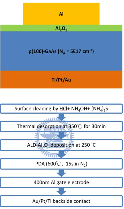
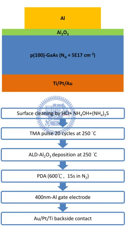
2.2 Sample Preparation
MOS capacitor sample was prepared on high Si-doped ( p-type, ~ 5×1017 cm-3 ) GaAs (100) substrates. At first, the GaAs was rinsed in the diluted HCl ( HCl : H2O = 1 : 3 ) solution for 3 min, followed by rinsed in deionized (D.I.) water for 5 min. Then, the GaAs was rinsed in the diluted NH4OH ( NH4OH : H2O = 1 : 10 ) solution for 10 min, followed by rinsed in D.I. water for 5 min. Third, the GaAs was rinsed in the (NH4)2S solution for 10 min, followed by rinsed in D.I. water for 5 min. After surface cleaning, thermal desorbed native oxide on the surface of substrate at 350 °C for 10 min and then the Al2O3 gate dielectric was deposited by atonic-layer-deposition (ALD) at 250 ℃, followed by post deposition annealing (PDA) at 600 °C for 15 s in a N2 ambient. Thermal evaporated 400 nm Al was patterned as gate electrodes through the lithography. Finally, Ti/Pt/Au ( 5 nm/30 nm/180 nm ) was
12
deposited by e-beam evaporator as backside contact. The complete process flow was shown in
Fig. 2.3. The electrical characteristics of Al/Al2O3/p-GaAs/TiPtAu MOS capacitors were measured using an HP4284 and HP4200, respectively.
2.3 Results and Discussion
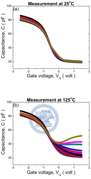
2.3.1 Multi-Frequency C-V of GaAs MOS Capacitor
In the beginning, exhibiting the basic properties of the GaAs MOS capacitor, C-V curves, include different measurement temperatures at 25℃ and 125℃, as shown in Fig. 2.4
(a) and (b), respectively. The frequency and temperature dependent C-V characteristic was
observed obviously because of Dit contribution which is distributed within the energy bandgap [6]. Besides, the quasi-static C-V was also shown in Fig. 2.5 and calculating the surface potential, ϕs, is a function of gate voltage. Berglund proposed [7]
ϕs 1 CQSCV
Cox
VG2
VG1
dVG
where CQSCV is the quasi-static C-V curve as a function of gate voltage. Integration from VG1 = VFB makes △ = 0, because band bending is zero at faltband. Integration from VFB to accumulation and from VFB to inversion gives the surface potential across the energy bandgap range. Fig. 2.6 illustrates the calculated result, surface potential versus gate voltage ( ϕs-VG ).
Utilizing high-frequency C-V curve and quasi-static C-V to extract Dit as a function of gate voltage by high-low frequency method is described in Eq. (2.12) [8].
Dit Cox q2 CQS Cox 1 CQS Cox Chf Cox 1 Chf Cox where the value of Cox is defined on accumulation of quasi-static C-V. After Dit extraction by high-low frequency method and x-axis conversion by surface potential as function of gate
13
voltage, result in Dit distribution within energy bandgap was displayed in Fig. 2.7.
2.3.2 Conductance Method Application of GaAs MOS Capacitor
Calculating the series resistance by Eq. (2.10) after measurement at 25℃. The result of series resistance extraction was shown in Fig. 2.8, and fitting the series resistance value, rs = 122 Ω. Next, correction of Cc and Gc by Eq. (2.8) and Eq. (2.9), respectively, and the plotting the Gp/ versus frequency by using Eq. (2.7). Fig. 2.9 (a) and (b) displayed Gp/ as a function of frequency through the correction of series resistance and calculation by conductance method. As same as before, plotting the Gp/ as a function of frequency curve which data was measured at 125℃ and the result was shown in Fig. 2.9 (c) and (d). Finally, getting the peak of Gp/ -frequency curve and determining the Dit by using Eq. (2.5). Fig.
2.10 illustrates the Dit distribution within energy bandgap as derived from measurement on GaAs MOS capacitor with ALD-Al2O3 gate dielectric.
2.3.3 Comparison of D
itExtraction
Fig. 2.11 presented the comparison of Dit extraction between high-low frequency method and conductance method on GaAs MOS capacitor with ALD-Al2O3 gate dielectric, and two Dit distributions from the different extraction methods have the same trends which indicate that the high value of Dit was close to mid-gap. The value of Dit from high-low frequency method is overestimated due to some detail; it may be the series resistance effect which has been neglected. Moreover, for high-frequency curve of high-low frequency method, the measurement must be sufficiently high to interface states do not respond, but for MOS capacitors with high Dit there will be some response due to interface traps. The conductance
14
method have the simplified but plentiful circuit model, combining multi-frequency C-V and elevated-temperature measurement enhance the sensitivity near mid-gap allowing the detection of trap energy levels [9].
2.4 Summary
After fabricating a MOS capacitor on GaAs substrates, we could have a standard operation process to extract the electrical characteristic of GaAs MOS capacitors with ALD-Al2O3 gate dielectric. At the first, we measured quasi-static C-V and the multi-frequencies of C-V at the different temperature conditions. Next, we calculated the surface potential as a function of gate voltage by Berglund’s integration. We can realize the fluctuation of Fermi level (EF) on the surface of GaAs substrate, and judge it weather reaches the inversion portion of the band gap or not. After Dit extraction by conductance method, we can accurately determine Dit distribution across the energy bandgap. Finally, utilizing the electrical characteristics of the GaAs MOS capacitor to decide the experimental condition is suitable in manufacture procedure of enhance-mode GaAs n-MOSFET.
15
Reference
[1] C.G.B. Garrett and W.H. Brattain. Physical theory of semiconductor surfaces. Physical
Review, vol. 99, p. 376-387, 1956.
[2] K. Lehovec. Frequency dependence of the impedance of distributed surface states in MOS structures. Appl. Phys. Lett., vol. 8, p. 48, 1966.
[3] E.H. Nicollian and A. Goetzberger. The Si/SiO2 interface - electrical properties as determined by the metal-insulator-silicon conductance technique. Bell Syst. Tech. J., vol. 46, p. 1055, December 1967.
[4] Nicollian and Brews. MOS (Metal Oxide Semiconductor) Physics and Technol-ogy., Wiley & Sons, New York, 1982.
[5] E.M. Vogel, W.K. Henson, C.A. Richter, and J.S. Suehle, “Limitation of Conductance to the Measurement of the Interface State Density of MOS Capacitors with Tunneling Gate Dielectrics,” IEEE Trans. Electron Dev., vol. 47, p. 601-608, March 2000; T.P. Ma and R.C.Barker, “Surface-State Spectra from Thick-oxide MOS Tunnel Junctions,”
Solid-State Electron. vol. 17, p. 913-929, Sept. 1974.
[6] G. Brammertz, H. C. Lin, K. Martens, D. Mercier, C. Merckling, J. Penaud,c C. Adelmann, S. Sioncke, W. E. Wang, M. Caymax, M. Meuris, and M. Heyns, “Capacitance–Voltage characterization of GaAs–Oxide Interfaces,” Journal of The
Electrochemical Society, vol.155, p. 945-950, 2008.
[7] C.N. Berglund, “Surface States at Steam-Grown Silicon-Silicon Dioxide Interfaces,” IEEE
Trans. Electron Dev., vol. 13, p. 701-703, Oct. 1966.
[8] R. Castagne and A. Vapaille, “Description of the SiO2-Si Interface Properties by Means of Very Low Frequency MOS Capacitance Measurements,“ Surf. Sci., vol. 28, p. 157-193, Nov. 1971.
16
[9] E. Duval and E. Lheurette, “Characterization of Charge Trapping at the Si-SiO2 (100) Interface Using high temperature Conductance Spectroscopy,” Microelectron. Eng., vol.65, p. 103-112, Jan. 2003.
17
Fig. 2.1 Equivalent circuits for conductance measurements; (a) MOS capacitor, (b) simplified circuit, (c) measured circuit, (d) including series rs resistance and tunnel conductance Gt. 0.0 0.2 0.4 0.6 0.8 1.0 1.2 1.4 10-2 10-1 100 101 102 103 104 105 106 107 108 109 EC
C
h
a
ra
cte
ri
sti
c fre
q
u
e
n
cy
( H
z )
Trap energy within bandgap ( eV )
25oC 90oC 125oC
EV
Fig. 2.2 Characteristic emission frequencies of trapped charge carriers in GaAs at the different temperatures.
18
Fig. 2.3 The structure and process flow of Al/Al2O3/p-GaAs (100)/TiPtAu MOS capacitor. Surface cleaning by HCl+ NH4OH+ (NH4)2S
Thermal desorption at 350℃ for 30min
ALD-Al2O3 deposition at 250 °C
PDA (600℃, 15s in N2)
400nm Al gate electrode
19 -3 -2 -1 0 1 2 20 40 60 80 100 Measurement at 25 o C C a p a ci ta n ce , C ( p F )
Gate voltage, VG ( volt ) (a) -3 -2 -1 0 1 2 20 40 60 80 100 Measurement at 125 o C C a p a ci ta n ce , C ( p F )
Gate voltage, VG ( volt ) (b)
Fig. 2.4 Multi-frequency C-V curve of Al/Al2O3/p-GaAs (100)/TiPtAu MOS capacitor at (a) 25℃, (b) 125℃measurement condition.
20 -3 -2 -1 0 1 2 20 40 60 80 100 Measurement at 25 o C C a p a ci ta n ce , C ( p F )
Gate voltage, VG ( volt )
Fig. 2.5 Quasi-static C-V curve of Al/Al2O3/p-GaAs (100)/TiPtAu MOS capacitor.
-2.0 -1.5 -1.0 -0.5 0.0 0.5 1.0 1.5 2.0 -0.2 0.0 0.2 0.4 0.6 0.8 1.0 1.2 1.4 EFB
Gate voltage, VG ( volt )
Ei Ev EC S u rfa ce p o te n tia l, s ( e V )
Fig. 2.6 Surface potential versus gate voltage of Al/Al2O3/p-GaAs (100)/TiPtAu MOS capacitor.
21 -0.2 0.0 0.2 0.4 0.6 0.8 1.0 1.2 1.4 1E12 1E13 1E14 EV D it ( 1 /e V cm 2 ) Surface potential, s ( eV ) EC
Fig. 2.7 Dit distribution by high-low frequency method of Al/Al2O3/p-GaAs (100)/TiPtAu MOS capacitor. 0.0 200.0k 400.0k 600.0k 800.0k 1.0M 0 200 400 600 800 1000 S e ri e s re si sta n ce , r s ( o h m s ) Frequency, f ( Hz ) rs = 122
22
Fig. 2.9 Gp/ as a function of frequency (a) and (b) at 25℃ measurement condition; (c) and (d) at 125℃ measurement condition.
100 1k 10k 100k 2E11 3E11 Frequency, f (Hz) G p /A q ( 1 /e V cm 2 ) Measurement at 25o C VG = -0.4 V VG = -0.35 V VG = -0.3 V VG = -0.25 V VG = -0.2 V 100 1k 10k 100k 4E11 6E11 8E11 Measurement at 125 o C Frequency, f (Hz) G p /A q ( 1 /e V cm 2 ) VG = -0.25 V VG = -0.2 V VG = -0.1 V VG = -0.05 V 100 1k 10k 100k 1E12 2E12 G p /A q ( 1 /e V cm 2 ) Measurement at 125o C Frequency, f (Hz) VG = -0.05 V VG = 0 V VG = 0.05 V VG = 0.1 V VG = 0.15 V VG = 0.2 V
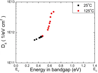
23 0.0 0.2 0.4 0.6 0.8 1.0 1.2 1.4 1E11 1E12 1E13 EC D it ( 1 /e V cm 2 )
Energy in bandgap (eV)
25oC 125oC
EV
Fig. 2.10 Dit distribution by conductance methods of Al/Al2O3/p-GaAs (100)/TiPtAu MOS capacitor. 0.0 0.2 0.4 0.6 0.8 1.0 1.2 1.4 1E11 1E12 1E13 1E14
EV Energy in bandgap (eV)
High-low frequency method Conductance method EC D it ( 1 /e V cm 2 )
24
Chapter 3
Optimization of Al
2
O
3
/GaAs
interface with MOS capacitor
3.1 Introduction
Today, in the semiconductor industry, Ⅲ-Ⅴ compound materials are used widely in such applications as optoelectronic devices, photodiodes, high-electron-mobility transistors (HEMTs), and other high-frequency devices. In order to obtain high-speed and low-power Ⅲ-Ⅴ metal-oxide-semiconductor (MOS) logic devices, a high quality interface between insulator and Ⅲ-Ⅴ is imperative. A large interface states density (Dit) within the Ⅲ-Ⅴ energy bandgap was caused by the native surface oxides is identified as a serious device challenge for Ⅲ-Ⅴ based devices [1-2]. Studies into competitive insulators on Ⅲ-Ⅴ compound semiconductors and efficient passivation methods have been performed for more than four decades; the poor quality of the insulator/substrate interface has been the prime obstacle hindering the realization of III-V MOS devices.
As mentioned in the chapter 1, GaAs is of great importance for scientific understanding of Ⅲ-Ⅴ compound material interfaces and GaAs MOS devices can be used as a sensitive test bed for all dielectric techniques. The treatment before insulator deposition or passivation layers between insulator and substrate techniques are developed on GaAs can naturally be applied to (In)GaAs or other Ⅲ-Ⅴ compound semiconductors [3]. Excluding SiO2 and Si3N4 ,
25
(Gd,Ga)2O3 , and HfO2 high-k dielectrics are also potential candidates for use on Ⅲ-Ⅴ compound substrates. One route of obtaining a native oxide-free interface that has attracted the attention of researchers is the “self-cleaning” [4-7]; in which the native oxides on GaAs get a reduction during the atomic layer deposition (ALD) of HfO2 or Al2O3 due to ALD precursor chemistry, tetrakis(ethylmethylamino)hafnium (TEMAH, Hf[N(C2H5)(CH3)]4) and trimethylaluminum (TMA, Al(CH3)3), separately. The self-cleaning during the ALD and the using of ultra-thin Si or Ge interfacial passivation layers are both practical techniques for improving the interface between insulator and Ⅲ-Ⅴ compound material. The pretreatment on GaAs by the ALD precursor prior to deposition of the gate dielectric has been reviewed comprehensively; the improvement in the device performance depends strongly on the ALD precursor pretreatment procedure. The in situ or ex situ deposition of several Si or Ge monolayers on GaAs can reduce the Dit to ca. 1×10¹⁰ –1×1011 cm-2 eV-1 [8-9]; this passivation technique has received renewed interest in recent years. Besides, the different crystalline surfaces of GaAs substrates were found that a much higher driving current on GaAs(111)A n-metal-oxide-semiconductor field-effect transistor (MOSFET). This experimental result conclusively demonstrated that Fermi-level (EF) pinning is not an intrinsic property of GaAs, but is orientation dependent [10].
Subsequent thermal annealing can further improve the quality of insulator films deposited on GaAs [11]. Meanwhile, during high temperature processing it is important to inhibit the loss of As within the GaAs substrate and also suppress the formation and subsequent incorporation of native oxides; these processes lead directly to electrical deterioration in GaAs MOS capacitors [12]. The impact of rapid thermal annealing ( RTA ) on the properties of various high-k/GaAs structures has been studied previously [13]. However, the correlations between these thermal reactions and the MOS performance have not been established in detail. In this study, we examined the electrical characteristics of
26
ALD-Al2O3 thin films deposited on an ALD precursor treated GaAs surface and then monitored the impact of postdeposition annealing (PDA) process. ALD is an ultrathin film deposition technique based on sequences of self-limiting surface reactions, which enables thickness control on the atomic scale. Unlike CVD, there is less need of reactant flux homogeneity, which gives large area capability, excellent conformality and reproducibility. Other advantages of ALD are the wide range of film materials available and high density. Also, lower deposition temperature can be used in order not to affect sensitive substrates.
The deposition mechanism of ALD is like chemical vapor deposition (CVD). We introduce the unique feature of the step-by-step deposition in ALD by using a general example of Al2O3 film deposition. It is well known that Al2O3 films can be grown by using alternating pulses of Al(CH3)3 (TMA, the aluminum precursor) and H2O (the oxygen precursor) in the presence of N2 carrier gas flow. Its mechanism procedures for one deposition cycle are illustrated in Fig. 3.1. At first, TMA is fed into the reactor and react with the OH bond on the GaAs substrate. Second, the reactor is purged with pure N2 gas to clean out residual TMA. Third, H2O is purged into the reactor and forms Al2O3 on surface. Finally, the reactor is purged with pure N2 gas again to clean out residual H2O.
3.2 Experimental Procedures
MOS capacitor structures were fabricated on high Si-doped ( p-type, ~ 5×1017 cm-3 ) GaAs substrates. At first, the sample was rinsed in the diluted HCl ( HCl : H2O = 1 : 3 ) solution for 3 min, followed by rinsed in deionized (D.I.) water for 5 min. Second, the sample was rinsed in the diluted NH4OH ( NH4OH : H2O = 1 : 10 ) solution for 10 min, followed by rinsed in D.I. water for 5 min. Third, the sample was rinsed in the (NH4)2S solution for 10 min, followed by rinsed in D.I. water for 5 min. After surface cleaning, the sample was loading
27
into the ALD chamber, followed by surface pretreatment with TMA 20 cycles pulse at 250 ℃. Next, the Al2O3 gate dielectric was deposited at 250 ℃, followed by PDA at 600 °C for 15 s in an N2 ambient. Thermal evaporated 400 nm Al was patterned as gate electrodes through the lithography. Finally, Ti/Pt/Au ( 5 nm/30 nm/180 nm ) was deposited by e-beam evaporator as backside contact. The complete process flow was shown in Fig. 3.2, and Tab.
3.1 shows experimental conditions. The electrical characteristics of Al/Al2O3/p-GaAs/TiPtAu MOS capacitors were measured using an HP4284 and HP4200, respectively.
Surface orientation Surface pretreatment ALD cycle PDA
(100) None Al2O3 60 cycles at 250℃ As-deposited 600℃ 15s in N2 TMA pulse 20 cycles
at 250℃
As-deposited 600℃ 15s in N2
(100)
TMA pulse 20 cycles at 250℃ Al2O3 150 cycles at 250℃ As-deposited 600℃ 15s in N2 (111)A As-deposited 600℃ 15s in N2 Tab. 3.1 The experimental condition of Si-doped ( p-type, ~ 5×1017 cm-3 ) GaAs MOS
28
3.3 Results and Discussion
3.3.1 TMA Effect
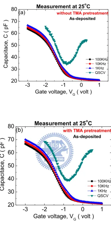
Fig. 3.3 ( a ) and ( b ) presented the frequency-dependent capacitance-voltage (C-V)
curves of Al/Al2O3/p-GaAs (100)/TiPtAu MOS capacitors with and without TMA pretreatment. According to Berglund’s integration as mentioned in the chapter 2, calculating the relation of surface potential fluctuation and gate voltage, and the result of TMA effect was shown in Fig. 3.4. The two curves revealed that the surface potential cannot reach conductance band (Ec) edge just only saturated near mid-gap; illustrated that the surface potential are pinned at mid-gap and gate voltage cannot product inversion charge, electron. Besides, in Fig. 3.5, utilizing high-low frequency method to extract the Dit distribution and comparing the trend of distribution within energy bandgap. In the Fig. 3.4, finding that surface potential fluctuation saturated at 0.7 eV above valance band (Ev) of GaAs, and this was corresponding to the Dit 1×10¹³ eV-1cm-2 in the Fig. 3.5.
Fig. 3.6 displayed the respective As 2p3/2 photoemission spectra of Al2O3/GaAs interface with/without TMA pretreatment and after wet cleaning. As the figure represents, we cannot found clearly that native oxide, As2O3 and As2O5, change between with and without TMA pretreatment obviously. This result of XPS analysis may be caused by some reasons, (a) the majority of self-cleaning effect by ALD reactions of TMA occurs following the initial TMA pulse [14]; (b) the XPS spectra analyzer with a nonmonochromatic Mg Kα x-ray source (hν=1253.6 eV), the energy source is too small that not finding the obvious reactions on the Al2O3/GaAs interface after additional 20-cycles TMA pulse.
Fig. 3.7 (a) and (b) represented the cross-section transmission electron microscopy
29
respectively. The interlayer between Al2O3 and Al is native oxide which is product after ligand exchange mechanism. During ALD process, the Al(CH3)3 was purged into the deposition chamber, it would react with the native oxides, i.e., As2Ox and Ga2Ox, and formed volatile products of As(CH3)3 and Ga(CH3)3, as shown by the following reactions.
Al CH3 3 As2Ox As CH3 3 Al2O3 Al CH3 3 Ga2Ox Ga CH3 3 Al2O3
The volatile products can be purged away in the next process of N2 purge. However, the volatility products may not be sufficiently high to be completely purged away by N2 purge, the remainder would be oxidized again in the followed pulse of water vapor and caused the contamination of As2Ox and Ga2Ox in the top portion of Al2O3, as observed in the Fig. 3.7. Hence, the interlayer between Al2O3 and Al can cause that lowering the value of k of the gate dielectric and raising the value of effective oxide thickness (EOT). Comparing Fig. 3.7 (a) and (b), the sample with TMA pretreatment has the larger value of k and the smaller value of EOT than the sample without TMA pretreatment.
3.3.2 PDA Effect
Fig. 3.8 presented the frequency-dependent C-V curves of Al/Al2O3/p-GaAs (100)/TiPtAu MOS capacitors with and without PDA. The sample with TMA pretreatment and PDA displayed a higher oxide capacitance accompanying a decreased C-V frequency dispersion, relative to as-deposited sample. Fig. 3.9 and Fig. 3.10 displayed the surface potential as function of gate voltage and Dit distribution within bandgap by high-low frequency method, respectively. These results were indicative of the slight abatement of the EF pinning effect in the capacitor properties; in other words, modulation of the carrier manipulation was enhanced.
30
In Fig. 3.11, using the conductance method by Eq. (2.5) to Eq. (2.10) as mentioned in the chapter 2 to extract accurately the Dit distribution, and the sample with TMA pretreatment and PDA had the lower value of Dit. Although not finding any reaction after the XPS analysis, we suggest that these As oxides (As2O3 and As2O5) convert to Ga2O3 by thermal conversion through PDA at 600 ℃ for 15 s in N2 ambient [15]. However, the electrical characteristics was improved, there was still very high value of Dit (Dit 1×10¹³ eV-1cm-2) at about 0.7 eV above Ev of GaAs by the result of high-low frequency method.
3.3.3 Surface Orientation Effect
Now that, having the better result that the GaAs MOS capacitor with TMA pretreatment and PDA process. We will study the electrical characteristic on GaAs (100) and (111)A MOS capacitors– two different crystalline surfaces with ALD-Al2O3 gate dielectric.
Fig. 3.12 illustrated the frequency-dependent C-V curves of Al/Al2O3/p-GaAs (100) and (111)A/TiPtAu MOS capacitors. Apparently, we could observe the less C-V stretch out behavior with the hump emerged in depletion region for p-GaAs (111)A sample, indicating the existence of a large Dit at the dielectric/substrate interface for p-GaAs (100) MOS capacitor. Not only utilizing the Berglund’s integration to calculate the surface potential fluctuation but also extracting Dit distribution by high-low frequency method as shown in Fig.
3.13 and Fig. 3.14, respectively. As the figures represented, the surface potential fluctuation
was improved very much and it could approach the conductance band, in other words, the EF not be pinned at mid-gap as the same as the before. This result was also verified by high-low frequency method, the value of Dit is about 2×10¹² eV-1cm-2 at mid-gap.
Since GaAs (111)A is a pure Ga polar surface in contrast to (100) Ga-As nonpolar surface, we presumed that the improvement of electrical characteristics is caused by the
31
different surface structure. One, As-S chemical bonds were broken at a relatively low temperature, approximately 150-250 ℃, whereas adsorption of sulfur from the surface, through breaking Ga-S bonds occurs above 500 ℃. At 250 ℃ ALD process, only Ga-S bonds remained stable, whereas As-S bonds were possibly reduced into the metallic As. So that, we could avoid the more arsenic oxide formation, which is believed that As-O will lead to high interface state density locate at the lower half of energy bandgap within GaAs.
Two, these electrical characteristics of experimental results may be explained by the following proposed empirical model as illustrated in Fig. 3.15. The empirical model is based on the unified disorder induced gap state (DIGS) model proposed by Hasegawa and Ohno in 1986 [15], which explains the striking correlation between the energy location E0 for the minimum interface state density at the insulator/semiconductor interface. The central concept is that there is an energy level called trap neutral level E0 at the insulator/GaAs interface, above which the trap states are of acceptor type or electron traps and below which are of donor type or hole traps. It is also explained that the GaAs (111)A sample have the better electrical characteristics, including the ability of surface potential fluctuation and the lower value of Dit at mid-gap of GaAs.
3.4 Summary
In this chapter, we studied sequentially self-clean effect by additional TMA pulse before Al2O3 deposition, PDA effect and surface orientation of substrate effect by analyzing the electrical characteristics of GaAs MOS capacitors. Utilizing the extraction of electrical characteristics as mentioned in the chapter 2, we demonstrated that the gate dielectric obtains the larger value of k and the smaller value of EOT by additional TMA pulse. After PDA process, the electrical characteristic of GaAs MOS capacitor was improved. Finally, we
32
investigated GaAs (100) and (111)A surface orientation by MOS capacitors. GaAs (111)A had the best surface potential fluctuation and the lower value of Dit at mid-gap, we proposed the chemical reactions on the surface of substrate during ALD and cited DISG model from reference to explain the improvement of electrical characteristics.
33
Reference
[1] C. L. Hinkle, A. M. Sonnet, E. M. Vogel, S. McDonnell, G. J. Hughes, M. Milojevic, B. Lee, F. S. Aguirre-Tostado, K. J. Choi, J. Kim, and R. M. Wallace, “Frequency Dispersion reduction and bond conversion on n-type GaAs by in situ surface oxide removal and passivation,” Appl. Phys. Lett., vol. 91, p. 183512, 2007.
[2] W. E. Spicer, N. Newman, C. J. Spindt, Z. Liliental‐ Weber, and E. R. Weber, “Pinning and Fermi level movement at GaAs surfaces and interfaces,” J. Vac. Sci. Technol. A, vol. 8, p. 2084, 1990.
[3] M. Xu, Y. Q. Wu, O. Koybasi, T. Shen, and P. D. Ye, “Metal-oxide-semiconductor field-effect transistors on GaAs (111)A surface with atomic-layer-deposited Al2O3 as gate dielectrics,” Appl. Phys. Lett., vol. 94, p. 212104, 2009.
[4] Martin M. Frank, Glen D. Wilk, Dmitri Starodub, Torgny Gustafsson, Eric Garfunkel, Yves J. Chabal, John Grazul, and David A. Muller, “HfO2 and Al2O3 gate dielectrics on GaAs grown by atomic layer deposition,” Appl. Phys. Lett., vol. 86, p. 152904, 2005. [5] C. L. Hinkle, A. M. Sonnet, E. M. Voge, S. McDonnel, G. J. Hughes, M. Milojevic, B.
Lee, F. S. Aguirre-Tostado, K. J. Choi, H. C. Kim, J. Kim, and R. M. Wallace, “GaAs interfacial self-cleaning by atomic layer deposition,” Appl. Phys. Lett., vol. 92, p. 071901, 2008.
[6] Hang Dong Lee, Tian Feng, Lei Yu, Daniel Mastrogiovanni, Alan Wan, Torgn Gustafsson, and Eric Garfunkel, “Reduction of native oxides on GaAs during atomic layer growth of Al2O3,” Appl. Phys. Lett., vol. 94, p.222108, 2009.
[7] M. Milojevic, C. L. Hinkle, F. S. Aguirre-Tostado, H. C. Kim, E. M. Vogel, J. Kim, and R. M. Wallace, “Half-cycle atomic layer deposition reaction studies of Al2O3 on (NH4)2S passivated GaAs 100 surfaces,” Appl. Phys. Lett., vol. 93, p.252905, 2008.
34
[8] D. S. L. Mui, D. Biswas, J. Reed, A. L. Demirel, S. Strite, and H. Morkoc, “Investigations of the Si3N4/Si/n-GaAs insulator-semiconductor interface with lowinterface trap density,” Appl. Phys. Lett., vol. 60, p. 2511, 1992.
[9] Z. Chen and D. Gong, “Physical and electrical properties of a Si3N4/Si/GaAs metal–insulator–semiconductor structure,” J. Appl. Phys., vol. 90, p. 4205, 2001.
[10] M. Xu, K. Xu, R. Contreras,) M. Milojevic, T. Shen, O. Koybasi, Y.Q. Wu, R.M. Wallace, and P. D. Ye, “New Insight into Fermi-Level Unpinning on GaAs: Impact of Different Surface Orientations,” Tech. Dig. Int. Electron Devices Meet., p. 865, 2009. [11] A. Jaouad, V. Aimez, C. Aktik, K. Bellatreche, and A. Souifi, “Fabrication of NH4)2S
passivated GaAs metal-insulator-semiconductor devices using low-frequency plasma- enhanced chemical vapor deposition,” J. Vac. Sci. Technol. A, vol. 22, p. 1027, 2004. [12] M.-K. Lee, C.-F. Yen, J.-J. Huang, and S.-H. Lin, “Electrical characteristics of
postmetallization-annealed MOCVD-TiO2 films on ammonium sulfide-treated GaAs,”
J. Electrochem. Soc., vol. 153, p. F266, 2006.
[13] M. Passlack, J. K. Abrokwah, Z. Yu, R. Droopad, C. Overgaard, H. Kawayoshi, “Thermally induced oxide crystallinity and interface destruction in Ga2O3–GaAs structures,” Appl. Phys. Lett., vol. 82, p. 1691, 2003.
[14] C. L. Hinkle, A. M. Sonnet, E. M. Vogel, S. McDonnell, G. J. Hughes, M. Milojevic, B. Lee, F. S. Aguirre-Tostado, K. J. Choi, H. C. Kim, J. Kim, and R. M. Wallace,” GaAs interfacial self-cleaning by atomic layer deposition,” Appl. Phys. Lett., vol. 92, p. 071901, 2008.
[15] H. Hasegawa and H. Ohno, ” Unified disorder induced gap state model for insulator- semiconductor and metal–semiconductor interfaces,” J. Vac. Sci. Technol. B, vol. 4, p. 1130, 1986.
35
36
Fig. 3.2 The structure and process flow of Al/Al2O3/GaAs/TiPtAu MOS capacitor. Surface cleaning by HCl+ NH4OH+(NH4)2S
TMA pulse 20 cycles at 250 °C
ALD-Al2O3 deposition at 250 °C
PDA (600℃, 15s in N2)
400nm-Al gate electrode
37 -3 -2 -1 0 1 20 30 40 50 60 70 80 Measurement at 25oC
without TMA pretreatment As-deposited C ap ac ita ce , C ( p F )
Gate voltage, VG ( volt )
100KHz 10KHz 1KHz QSCV (a) -3 -2 -1 0 1 20 30 40 50 60 70 80 (b) Measurement at 25 o C
with TMA pretreatment
As-deposited C a p a ci ta ce , C ( p F )
Gate voltage, VG ( volt )
100KHz 10KHz 1KHz QSCV
Fig. 3.3 Frequency-dependent C-V curves of Al/Al2O3/p(100)-GaAs/TiPtAu MOS capacitors. (a)without, (b)with TMA pretreatment.
38 -0.5 0.0 0.5 1.0 1.5 2.0 -0.2 0.0 0.2 0.4 0.6 0.8 1.0 1.2 1.4 Ei Ev EC S u rfa ce p o te n tia l, s (e V ) VG-VFB ( volt )
without TMA pulse with TMA pulse
Fig. 3.4 Comparison of surface potential fluctuation of TMA effect of Al/Al2O3/p-GaAs (100)/TiPtAu MOS capacitors.
0.0 0.2 0.4 0.6 0.8 1.0 1.2 1.4 1E12 1E13 1E14 D it ( 1 /e V cm 2 ) Surface potential, s ( eV ) without TMA pulse with TMA pulse
Fig. 3.5 Comparison of Dit distribution of TMA effect of Al/Al2O3/p-GaAs (100)/TiPtAu MOS capacitors.
39 38 40 42 44 46 0.0 0.2 0.4 0.6 0.8 1.0 1.2 As2O5 As2O3 As0 As-Ga As 3d In te n si ty( a .u .) Binding energy ( eV ) After wet clean
Without TMA pretreatment WithTMA pretreatment
Fig. 3.6 As 2p3/2 XPS spectra of Al2O3/GaAs interface subjected to with and without TMA pulse.
40
Fig. 3.7 The cross-section of TEM image of Al/Al2O3/GaAs : (a) without TMA pretreatment; (b) with TMA pretreatment.
41 -3 -2 -1 0 1 20 30 40 50 60 70 80 100k Hz 10k Hz 1k Hz Quasi-static Measurement at 25oC
with TMA pretreatment
PDA, 600o C 15s in N2 C a p a ci ta ce , C ( p F )
Gate voltage, VG ( volt ) (b)
Fig. 3.8 Frequency-dependent C-V curves of Al/Al2O3/p(100)-GaAs/TiPtAu MOS capacitors at 25℃ and 125℃measurement condition with TMA pretreatment, (a) and (c) as-deposited; (b) and (d) with PDA.
-3 -2 -1 0 1 2 20 30 40 50 60 70 80 Measurement at 125oC
with TMA pretreatment
PDA, 600o C 15s in N2 100k Hz 10k Hz 1k Hz C a p a ci ta n ce , C ( p F )
Gate voltage, VG ( volt ) (d) -3 -2 -1 0 1 2 20 30 40 50 60 70 80 Measurement at 125oC
with TMA pretreatment
As-deposited C a p a ci ta n ce , C ( p F )
Gate voltage, VG ( volt )
100k Hz 10k Hz 1k Hz (c) -3 -2 -1 0 1 20 30 40 50 60 70 80 (a) Measurement at 25oC
with TMA pretreatment
As-deposited C a p a ci ta ce , C ( p F )
Gate voltage, VG ( volt )
100k Hz 10k Hz 1k Hz Quasi-static
42 -0.5 0.0 0.5 1.0 1.5 2.0 2.5 -0.2 0.0 0.2 0.4 0.6 0.8 1.0 1.2 1.4 Ev Ei EC VG-VFB ( volt ) S u rfa ce p o te n tia l, s (e V
) with TMA and PDA
with TMA and as-deposited
Fig. 3.9 Comparison of surface potential fluctuation of Al/Al2O3/p-GaAs (100)/TiPtAu MOS capacitors with and without PDA.
0.0 0.2 0.4 0.6 0.8 1.0 1.2 1.4 1E12 1E13 1E14 Ev EC
with TMA and PDA with TMA and as-deposited
D it ( 1 /e V cm 2 )
Surface potential, s (eV)
Fig. 3.10 Comparison of Dit distribution of Al/Al2O3/p-GaAs (100)/TiPtAu MOS capacitors with and without PDA.
43 0.0 0.2 0.4 0.6 0.8 1.0 1.2 1.4 1E11 1E12 1E13 1E14 D it (1 /e V cm 2 ) Surface potential ( eV ) with TMA and PDA with TMA and as-deposited
Fig. 3.11 Comparison of Dit distribution of Al/Al2O3/p-GaAs (100)/TiPtAu MOS capacitors with and without PDA.
44 -4 -3 -2 -1 0 1 2 20 30 40 50 p-GaAs (100)
with TMA pretreatment
PDA 600oC 15s N2 Measurement at 25oC C a p a ci ta n ce , C ( p F )
Gate voltage, VG ( volt ) 100KHz 10KHz 1KHz QSCV (a) -4 -3 -2 -1 0 1 2 3 20 30 40 50 Measurement at 25 o C p-GaAs (111)A
with TMA pretreatment
PDA 600oC 15s N2 ca p a ci ta a n ce , C ( p F )
Gate voltage, VG ( volt ) 100KHz
10KHz 1KHz QSCV (b)
Fig. 3.12 C-V curves of Al/Al2O3/p-GaAs/TiPtAu MOS capacitors (a) (100), (b) (111)A surface orientation.