行政院國家科學委員會專題研究計畫 期中進度報告
子計畫七:奈米結構氧化物光子晶體材料製程與光電特性研
究(2/3)
計畫類別: 整合型計畫 計畫編號: NSC92-2216-E-009-014- 執行期間: 92 年 08 月 01 日至 93 年 07 月 31 日 執行單位: 國立交通大學材料科學與工程學系 計畫主持人: 陳三元 報告類型: 精簡報告 處理方式: 本計畫可公開查詢中 華 民 國 93 年 9 月 14 日
奈米結構氧化物光子晶體材料製程與光電特性研究(2/3)
Growth kinetics and microstructure evolution of well-aligned and patterned ZnO nanorods on Si-based substrate in aqueous solution
計畫編號:NSC92-2216-E-009-014 執行時間:92/08/01 ~ 93/07/31 主持人:陳三元 教授 交通大學材料科學與工程學系 中文摘要 本研究首先主要是在探討在低溫下單晶 ZnO 奈米柱的成長動力學和微結構的發展。在不 同特性基版上的 ZnO 奈米線會表現出不同的 成長行為和方向。在純 Si 基版上,ZnO 奈米 線會散亂地沿著(100)優選平面或 [01 1 0] 成長方向,排列在整個基版上。由高解析穿 透式電子顯微鏡(HRTEM)觀查可得到,散亂的 ZnO 奈米線其實是自我組裝的兩階段式成長 所得到。相對的,當成長在 ZnO film/Si 的 基版上,規則排列的 ZnO 奈米線則會直接從 ZnO film 上沿著[0002]方向成長。具有較大 的長寬比(l/w),可以達到 25 到 30。並且發 現有些奈米柱產生一些平面缺陷,例如疊差 (stacking faults)。這些現象暗示著,從溶 液成長的規則排列 ZnO 奈米線不是直接跟基 版有關,而是跟基版的表面的凹凸率直接相 關 。 因 而 本 研 究 在 後 期 則 進 一 步 利 用 PS beads 在 Si 或 Polycarbonate 基板,來製作 patterned ZnO 奈米柱以研究其奈米結構在 光子晶體之光電特性。 關鍵字: ZnO 奈米柱、成長動力學、微結構 發展、方向性排列 Abstract
Growth kinetics and microstructure evolution of single-crystal ZnO nanorods (ZNs) synthesized in aqueous solutions at low temperatures were investigated. Depending on surface characteristics of substrate, ZNs present different growth behavior and direction. On pure Si substrate, ZNs were scattered over the entire Si substrate with a preferred orientation in the (100) plane or grown along [011 0]
direction. HRTEM observation demonstrates that the scattered ZNs present two-stage growth process with a self-assembly process of ZNs in the later growth stage. In contrast, on Si wafer with ZnO film coated, well-aligned ZNs were
directly grown along [0002] direction from the ZnO film on Si. In comparison with the scattered ZNs, a larger aspect ratio (length/width) up to 25-30 was obtained for the well-aligned ZNs. In addition, some planar defects such as stacking faults were probably resulted due to faster growth of ZnO growth unit in the later growth stage. These observations and findings imply that the growth of the well-aligned ZNs from the soft solution is not related to the used substrates but strongly influenced by the surface characteristics as well as roughness of the substrate.
Keywords: ZnO nanorods ; Growth kinetics ; Microstructure evolution ; well-aligned
I. Introduction
One-dimensional (1D) nanostructures have great potential for learning the fundamental concepts of the roles of both dimensionality and size in physical properties as well as for application in nanodevices and functional materials. Other than carbon nanotubes, 1D nanostructures such as nanowires are ideal systems for investigating the dependence of electrical transport, optical and mechanical properties on size and dimensionality.[1]
Zinc oxide (ZnO) is an important electronic and photonic material because of its wide and direct band gap (∆Eg = 3.37eV) material.[2]
The strong exciton binding energy of ZnO (60meV) is much larger than that of GaN (~ 25meV), which can ensure an efficient exciton emission at room temperature.[2] Recently, highly oriented nanorod array of ZnO nanostructures have demonstrated their potential applications in manufacturing electronic and optoelectronic devices.[3-5]
Various methods including chemical, electrochemical, and physical deposition techniques have been employed to synthesize 1D ZnO nanostructures such as catalytic
growth via the vapor-liquid-solid (VSL) epitaxial method[6] and metal-organic-chemical vapor deposition (MOCVD).[7-8] However, those methods are expensive and energy consuming processes since they are operated under extreme conditions. It is well conceived that preparation of ZnO via solution chemical routes provides a promising option for large-scale production of this materials. Although wet-chemical approaches have been used for large oriented arrays of ZnO nanorods on polycrystalline (or single-crystalline) substrates from aqueous solutions[9-10], it is worth noting that without suitable treatment on the substrate, highly oriented ZnO nanorods grown on a Si wafer has been rarely achieved due to the larger mismatich (~40%) between the substrate and the ZnO nanorods.
Yamabi et al. reported that without undercoats on the surface, clusters of spindle-shaped hexagonal crystallite with diameters of 0.5-1.0 um were scattered over the surface of a silicon wafer, but highly aligned arrays of ZnO nanorods with diameters of 20-100 nm can be developed on Si substrate undercoated with Zn(Ac)2 and annealed at
500oC.[10] Recently, Choy et al. also found that high-quality ZnO nanorods were successfully grown on a Si wafer by a wet-chemical process at 95oC for 6 h, where the Si wafer was dip-coated with 4 nm sized ZnO nanoparticles as a buffer and seed layer prior to crystal growth.[11] These observations reveal the importance of surface characteristics or treatment in the growth of well-oriented ZnO nanorods in aqueous solution. However, little investigation was paid attention to the growth behavior and kinetics of such ZnO nanorods, in particular to tailor their orientation onto the substrates, that can be used to control the structure morphology and optoelectronic properties.
Therefore, in this work, a simple wet-chemical method was used to study the growth kinetic of both scattered and aligned ZnO nanorods on Si by monitoring the average aspect ratio of ZnO nanorods as a function as growth time in aqueous solution. By controlling the experimental conditions, well-aligned arrays of ZnO nanorods with different aspect ratios can be obtained. Moreover, high-resolution transmission
electron microscopy (HRTEM) was performed to investigate the growth mechanisms of ZnO nanorods.
II. Experimental
Zinc nitrate hexahydrate (Zn(NO3)2.6H2O) was
used as the Zinc precursors to synthesize the ZnO nanorods (ZNs). Methenamine (C6H12N4),
also called hexamethylenetetramine (HMT) is a highly water soluble, non-ionic tetradentate cyclic tertiary amine and used to comply simultaneously with the precipitation of the divalent post-transition metal Zn2+ ions, the nucleation growth of its stable oxide form, zincite ZnO. Three kinds of substrates were also used for comparison in this study. One is Si and the other is Si coated with ZnO film. In addition, polymer-based substrate such as polystyrene (PS)/polycarbonate (PC) is also used in this work. The ZnO thin films were deposited on Si substrates by rf magnetron sputtering following our previous report.[12] An equimolar (0.02M) aqueous solution of Zn(NO3)2.6H2O and HMT was prepared in a
bottle. Subsequently, substrates were placed inside the aqueous solutions and heated at ambient temperature (55-95oC) for 0.1-15 h. After that, the substrates were removed from the aqueous solutions, rinsed with distilled water, and dried at room temperature overnight.
X-ray diffractometer (M18XHF, MAC Science, Tokyo, Japan) was used to examine the crystalline phase of the synthesized compounds with a scanning rate 4° (2θ) per min over a 2θ range 20- 60°. The morphology
of the ZnO nanorods was examined by scanning electron microscopy (SEM, Hitachi model S4000). Microstructure observation was performed by transmission electron microscopy (TEM) with a Philips Tecnai 20 instrument (Holland, The Nertherlands), operated at 200 keV. A double-tilt specimen holder was used to tilt several zone-axes. High-resolution images were recorded at several exact zone-axes with Scherzer defocus at –67nm and at an electron-optical magnification of 490000 to 520000.
III. Results and discussion
3.1 Phase and morphology of ZnO nanorods grown on different substrates
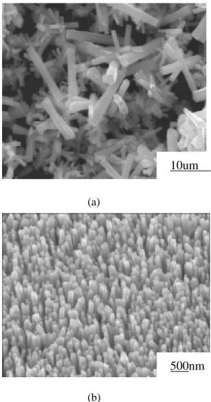
ZnO-coated polycarbonate (PC), were used in this work to study the growth behavior of ZnO nanorods (ZNs) in the precursor solution at different temperatures of 55-95oC for several hours. No ZNs were observed below 50oC, indicating a thermal barrier for the growth of ZNs can not be overcome. Above 95oC, ZNs can not be synthesized because the reaction temperature is near to its melting point of the aqueous solution. Figure 1 shows the SEM images of the as-synthesized ZNs grown on these two kinds of substrates at 75oC for 10 h in the 0.02M solution. As shown in Fig. 1(a), ZNs with the dimension of 7-10 µm in length and 0.5-1 µm in diameterwere scatteredon the Si substrate. On the other hand, high density of well-aligned ZNs with dimensions of 20-200 nm in diameter and up to several µm in length were obtained uniformly when ZNs were grown on ZnOf/Si as shown in Fig. 1(b). It
seems to imply that the formation of well-aligned ZNs on a pure Si substrate is difficult because a large mismatch (~40%) exists between ZnO and Si. Based on this reason, this would retard the nucleation of ZnO on Si substrate. Consequently, it strongly reveals the importance of the substrate characterization on the growth behavior of ZNs in the aqueous solution.
The X-ray diffraction patterns (XRD) show that the ZnO crystal phase starts to appear at 50oC and well crystallized above 65oC. As shown in Fig. 2(a) and (b), a strongly oriented peak can be indexed as the wurtzite ZnO at 75oC in 0.02 M aqueous solutions for the ZNs grown on Si and ZnOf/Si substrate. However, it
should be pointed out that a remarkable difference in XRD patterns exists between those two substrates. As shown in Fig. 1(a), the diffraction peaks were indexed as (100), (002) and (101) planes of ZnO for the ZNs grown on Si substrate. On the other hand, Fig. 2(b) illustrates that the strongest diffraction peak corresponding to the (002) plane of ZnO was detected when the ZNs were grown on ZnOf/Si
substrate. These observations obviously imply different growth behavior between (100)-oriented (called as scattered) ZNs on Si and (002)-oriented (called as aligned) ZNs on ZnOf/Si.
3.2. Microstructural analysis of ZnO
nanorods
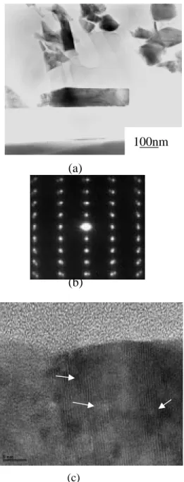
It is well known that ZnO has as a hexagonal lattice with c/a axial ratio of 1.602.[13] The most commonly observed morphologies of ZnO are either rod-like or needle-like crystals, especially prepared ZnO in aqueous solution because of anisotropic crystal growth. The transmission electron microscopy (TEM) bright-field (BF) image and corresponding selected-area diffraction (SAD) pattern of the scattered ZNs are shown in Fig. 3(a) and (b), respectively. The SADP in Fig. 3(b) clearly indicates that the scattered ZNs were grown along [011 0] direction. This result is also
inconsistence with the XRD analysis that the ZNs are preferentially oriented along [011 0] direction. A close examination of the SADP in Fig. 3(b) shows the split of diffraction spots and extra diffraction spots, located at halfway between the central (000) spot, the {0002} spots and {01 1 0} spots. However, no Morié fringes were observed in the corresponding High-resolution TEM (HRTEM) in Fig. 3(c) so that double diffraction can be neglected in this study.
Since the crystallographic phase of these ZNs belongs to wurtzite structure with a space group of P63mc, it easily appears as a
characteristic “zigzag” structure,[14-15] so-called “superlattice diffraction”, corresponding to the observed extra spots in the SADP. It seems to imply that the crystal structure of the scattered ZNs was constituted from many tiny areas such as domains or mosaic texture according to the disoriented few degrees in SADP. It is well known that a crystal with mosaic structure does not have its atoms arranged on a perfectly regular lattice extending from one side of the crystal to the other; instead, the lattice is broken up into a number of tiny blocks, each slightly disoriented one from another. Within these tiny blocks, there exists a structural mismatch at the interface between these domains.[16] This mismatch may be very small and involve a difference in angular orientation between the domains as in our case with 1~2° difference in the SADP. Furthermore, HRTEM image in Fig. 3(c) recorded from this scattered ZN reveals that there seem to be two types of lattice fringes in this HRTEM image: one with wave-like fringes (as arrowed in Fig. 3(c)) and the other with straight fringes. This variation of
lattice fringes as marked with arrows seems to be caused by these two types of crystal arrangements.
Figure 4(a) shows the TEM bright-field (BF) image of the aligned ZNs grown on ZnOf/Si
substrate. In contrast to the scattered ZNs, most of the ZNs were grown in a direction perpendicular to the ZnOf/Si substrate. 4(b). A
higher magnification in Fig. 4(b) indicates that the lattice fringes are perpendicular to the longitude direction of the ZNs, and the singular fringe spacing is about 0.51nm, which is nearly consistent with the c-axis parameter in hexagonal ZnO structure (c= 0.521nm in ZnO structure). This demonstrates that [0002] direction is the preferred growth direction for the well-aligned ZNs. In addition, as one pays attention to the interface between ZNs and ZnOf/Si shown in Fig. 4(c), it was observed
that the well-aligned ZNs seem to be grown from the cup tip near the grain boundary between two ZnO grains in ZnO film. The formation of the cup shape around grain boundary between two ZnO grains is supposed to be correlated with the solution reaction during the nucleation and growth of ZNs. This demonstrates that the cup tip probably becomes a preferential nucleation position for the well-aligned ZNs grown on ZnOf/Si. However,
in addition to (0002) fringes, some ZNs with white lines dissecting the ZNs can be occasionally identified as marked with arrows in Fig. 5. This kind of planar defects can be considered as extrinsic stacking faults with insertion of an extra Zn-O layer parallel to the basal plane. It was worth noting that the presence of (0001) stacking faults provides a possible diffusion path to modify its optoelectronic properties according to our study.
[17]
However, well-aligned ZnO nanorods without any planar defects can be also obtained in aqueous solution by controlling the experimental conditions.
3.3 Growth behavior and kinetics of ZnO nanorods
It is well known that the growth behavior of ZNs was strongly influenced by the growth conditions such as ion concentration in solutions, reaction temperature and time. As illustrated in Fig. 6, the aspect ratios (AR =length/width) of ZNs grown on Si and
ZnOf/Si substrate as a function of growth time
at 75oC were measured.
When the Si substrate without ZnO film coated was placed in the Zn-containing aqueous solution, in the initial growth stage of ZNs, prior to 0.2h, no obvious ZNs can be detected. However, above that (0.2-0.3h), it can be observed that a small amount of ZNs with ~20 nm in diameter and ~60 nm in length were randomly scattered on Si substrate according to SEM images (not shown here). However, at the same period of growth time, no any well-aligned ZNs can be clearly observed from the Si substrate. It seems to imply that the formation of well-aligned ZNs on a Si substrate is difficult based on the lattice parameters of ZnO and Si because a large mismatch (~40%) exists between ZnO and Si and this would retard the nucleation of ZnO on Si substrate. This phenomenon reveals that the well-aligned ZNs remain in the nucleation stage, but the scattered ZNs are going through nucleation and growth stage. Until 0.5 h, the well-aligned ZNs can be clearly obtained but the scattered ZNs have been grown with an AR of 2-3. Subsequently, with an increase of growth time, it can be observed that the increasing rate of the AR becomes slower in the scattered ZNs as compared to that in the well-aligned ZNs. Especially, above 5 h, the AR for the scattered ZNs remain unchanged with a constant of about 9-11 but the AR is also slightly decreased with increasing growth time up to 15 h. This implies that the scattered ZNs did not further grow as expected despite extending growth time. As evidenced from the TEM BF image and corresponding SADP of ZNs grown for 5 h in Fig. 7, it seems to indicate that more than two ZNs with the same [01 1 0] growth
direction were self-assembled together to form a bundle. The TEM dark-field (DF) image clearly reveals that more than two ZNs were aggregated in a coplanar manner using their side planes to form a large ZN as shown in Fig. 7(c). This bundle ZNs can be further transformed into another ZN with a larger dimension in diameter. In other words, the side crystal planes of the ZNs were able to glue together to form a larger crystal. This behavior is also called “oriented attachment”.[18] Based on viewpoint of thermodynamic, this self-assembling process is possible for the
synthesized ZNs to reduce total Gibbs free energy in the later growth stage. This phenomenon is very similar to the Ostwald ripening occurring in ceramic sintering progress. This observation may be used to explain the slight decrease in AR in the later growth stage (5 -15 h). Consequently, the growth behavior of the scattered ZNs can be considered as a two-step growth mechanism.
In contrast, as the ZnOf/Si substrate was
used and immersed into the precursor solution for the growth of ZNs, it was found that in the early stage (t < 0.5), no aligned ZNs can not be clearly observed from the ZnOf/Si substrates
but at t = 1 h, a smaller AR was obtained for the well-aligned ZNs compared to that of scattered ZNs. It was believed that the ZnO nuclei will be preferentially grown on the ZnOf/Si substrate in this stage and the
promotion of heterogeneous nucleation is ascribed to the high affinity of the nuclei of ZnO for the surface, especially formed at the cup sites as shown in Fig. 4(c). In this condition, although an inherent asymmetry along the c axis allows the anisotropic growth of the crystal along the [0002] direction, the lateral growth along different directions are possible for the nucleus to decrease the roughness of the film surface because of surface energy effect. When the favorable nucleation position of ZN was formed on the ZnO film, ZnO growth unit (or called coordination polyhedron) will stack in order and grow along [0002] direction. Subsequently, a fast growth along longitudinal direction (c-axis) for the well-aligned ZNs was expected because the growth in width direction is suppressed due to the size of cup shape in ZnOf/Si substrate. In 15 h, well-aligned and
highly oriented ZNs with an aspect ratio up to 25-30 can be obtained. These results can be used to explain the observation that the well-aligned ZNs with a smaller AR were formed in an early stage but later, the ZNs were rapidly grown along the longitudinal direction in the later growth stage. Therefore, in this condition, some stacking faults are accidentally observed as shown in Fig. 5 that is probably due to faster stacking and the instability of the polar (002) plane in ZnO.
3.4 Growth of patterned ZnO nanorods on
polystyrene (PS)/polycarbonate (PC) substrates
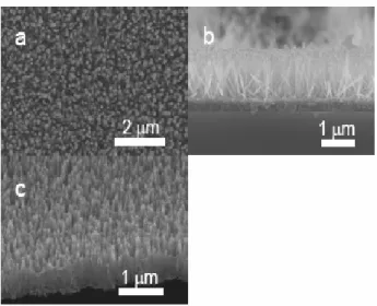
Figure 8(a) shows the surface images of large-scale arrayed ZnO nanorods grown on polystyrene (PS)/polycarbonate (PC) substrates. It was found that the ZnO nanorods have a well-defined hexagonal plane with a homogeneous diameter of approximately ~60 nm due to uniform growth rate. The cross-section image in Figure 8(b) shows that the ZnO nanorods with a uniform length of 1.5 µm are directionally and densely grown over the entire PS surface of the substrates. Furthermore, we found that the patterned ZnO nanorods (Fig. 8(c)) can be developed after the removal of the PS beads in the specimen produced by the same conditions as Fig 8(b). It implies that the PS layers can act as a nucleation base to supply the appropriate environment to increase the probability of the high density of nucleation sites and enhance the crystal growth.
To understand how the well-aligned arrays of oriented ZnO nanorods were formed on the organic substrates, the sample was further investigated by SEM and TEM. Three stages can be identified for the growth of ZnO nanorods on PS layers. The first initial stage (t < 0.5 h) is the induction time, during which an ultra-thin monolayer was slowly generated under the surface of PS beads in the solution. It is difficultly observed by SEM microscopy but the ultra-thin monolayer can be simply detected to be ZnO signal by chemical analysis such as X-ray photon spectroscopy (not shown) after removing the PS beads. The second stage is the nucleation period, during which the concentration of the building units in the solution builds up until a critical super-saturation level is reached and then nucleation occurs (Fig. 9(a)). It was believed that the ZnO nuclei will be preferentially grown on the concave regions of PS layers in this stage and the promotion of heterogeneous nucleation is ascribed to the high affinity of the ZnO nuclei to the PS surface. After nucleation, in the third period, a fast growth along longitudinal direction (c-axis) for the oriented ZnO nanorods was expected because the growth in width direction is suppressed due to the size of concave shape in PS layers as shown in Fig. 9(b). Figure 9(c) shows the high
resolution TEM (HRTEM) image of the well-aligned ZnO nanorods grown on PS/PC substrates. It indicates that the lattice fringes are perpendicular to the longitude direction of the ZnO nanorods, and the singular fringe spacing is about 0.51nm, which is nearly consistent with the c-axis parameter in hexagonal ZnO structure (c= 0.521nm in Wurtzite ZnO). This demonstrates that <001> direction is the preferred growth direction for the well-aligned ZnO nanorods. Recently, it was reported the aligned ZnO nanorods can be grown on the Si substrates with ZnO buffered layers which consists of nanoparticles or crystalline films.16,17 However, most reports in the literature ignored the effect of surface morphology on the nucleation base of the aligned ZnO nanorods. Therefore, a HRTEM analysis was paid attention to the interface between ZnO nanorods and ZnO monolayer (~5 nm thicker) shown in Fig. 9(d) after removing the PS beads. It was observed that the well-aligned ZnO nanorods seem to be grown from the concave tip near the grain boundary between two ZnO grains in ZnO monolayer. A detail investigation for the growth behavior and kinetics of ZnO nanorods grown on inorganic substrates were reported in our previous study.19 This demonstrates that the well-aligned ZnO nanorods can be grown on organic and inorganic substrates with controlled surface morphology.
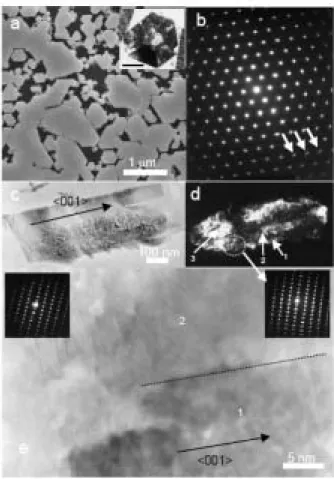
Figure 10(a) presents the SEM surface image of ZnO nanorods grown on organic substrates more than 24h. It was found that the ZnO nanorods begin to amalgamate with other neighboring nanorods and their growth becomes physically limited. In comparison with Fig. 8(a), the ZnO rods become much thicker (more than 0.5 µm) but not much longer (about 1.7 µm) after long-term growth because the ZnO nanorods have started on coalescence process with adjacent rods. Therefore, after the lateral growth begins, the growth rate of ZnO nanorods in the <001> orientation would obviously decrease. The TEM bright-field (BF) image (inset in Figure 10(a)) of the <001> zone-axis of (cross-sectional) ZnO nanorods clearly illustrated the merged grains with side crystal plane attached. Moreover, as confirmed by Figure 10(b) for the <001> zone-axis selected-area electron diffraction (SAED)
pattern of ZnO nanorods. The split diffraction spots in the edge region (marked with arrows) of the SAED pattern suggest that the merged ZnO nanords are not perfectly aligned in both a and b directions. The longitudinal direction is along the c <001> orientation. The TEM images in Fig. 10(c) and d reveal the BF and dark-field (DF) images of the merged ZnO nanorods, respectively. The DF image in Fig. 10(d) clearly and visibly shows that more than two ZnO nanorods were aggregated in a coplanar manner using their side planes to form a larger ZnO nanorod. A magnified picture of Fig. 10(c) was illustrated in Fig. 10(e). The insets in the left and right of Figure 10(e) present the SAED patterns of single and couple nanorods in coalescent ZnO nanorods, respectively. The split diffraction spots were also identified from the couple rods and a slight misalignment between nanorods was observed. The growth behavior of the larger ZnO nanorods in later long-term growth can be considered from direct combination of a small number of individual nanorods which was similar to oriented attachment.
IV. Conclusion
We have developed a low-temperature synthetic route to prepare well-aligned arrays of oriented ZnO nanorods with high crystallinity in the diameter of ~60 nm on the Si substrates. Single-crystal ZnO nanorods (ZNs) can be synthesized in an aqueous solution at 75oC. Depending on the surface characteristics of the substrate, ZNs present different growth behavior and direction. On pure Si substrate, ZNs were scattered over the entire Si substrate with a preferred orientation in the (100) plane or grown along [011 0]
direction. HRTEM observation demonstrates that the scattered ZNs present two-stage growth process with a self-assembly process of ZNs in the later growth stage. In contrast, on Si wafer with ZnO film coated, well-aligned ZNs were directly grown along [0002] direction from the ZnO film on Si. In comparison with the AR of the scattered ZNs, a larger AR up to 25-30 was obtained. Although the surface characteristics of the substrates plays a very important role in both scattered and well-aligned growth of the ZNs, the ZnO film on Si wafer is surely to reduce the mismatch between the Si substrate
20 30 40 50 60 (010) (100) (002) (a) (b) Intensity (a. u.) 2θ
and the ZnO nanorods. This simple approach should promise us a future large-scale synthesis of the patterned growth of the highly well-aligned ZNs on various kinds of substrates buffered with a controlled morphology and roughness layer in an aqueous solution at low temperatures.
Acknowledgments
This work was financially supported by the National Science Council of the Republic of China, Taiwan under Contract No. NSC-92-2216-E-009-014.
References
(1) Hu, J.; Odom, T. W.; Lieber, C. M. Acc.
Chem. Res. 1999, 32, 435.
(2) Zamfirescu, M.; Kavokin, A.; Gil, B.; Malpuech, G.; Kaliteevski, M. Phys. Rev. B.
2002, 65, 161205.
(3) Lieber, C. M.; Cui, Y. Science 2001, 291,
851.
(4) Duan, X.; Huang, Y.; Cui, Y.; Wang, J.; Lieber, C. M. Nature 2001, 409, 66.
(5) Park, W. I.; Yi, G.; Kim, M.; Pennycook, S. J. Adv. Mater. 2003, 15, 526.
(6) Wu, Y.; Yang, P. J. Am. Chem. Soc. 2001,
123, 3156.
(7) Chiou, W. T.; Wu, W. Y.; Ting, J. M. Diam.
Relat. Mater. 2003, 12[10-11], 1841.
(8) Lee, C. J.; Lee, T. J.; Lyu, S. C.; Zhang, Y.; Ruh, H.; Lee, H. J. Appl. Phys. Lett. 2002,
19, 3648.
(9) Vayssieres, L.; Keis, K. J. Phys. Chem. B
2001, 105, 3350-3352
(10) Yamabi, S.; Imai, H. J. Mater. Chem.
2002, 12, 3773
(11) Choy, J. H.; Jang, E. S. Adv. Mater. 2003,
15, 1911
(12) Lin, C. C.; Hsiao, C. S.; Chen, S. Y.; Cheng, S. Y. J. Electrochem. Soc. 2004,
in press.
(13) Bailar, J. C.; Emeleus, H. J.; Nyholm, R. and Trotman-Dickenson, A. F. Comprehensive inorganic chemistry, vol. 3. Pergamon Press, Oxford, 1975.
(14) Manna, L.; Scher, E. C.; Alivisatos, A. P. J.
Am. Chem. Soc. 2000, 122, 12700.
(15) Trentler, T. J; Hickman, K. M.; Goel, S. C.; Viano, A. M.; Gibbson, P. C.; Buhro, W. E. Science 1995,
270, 1791.
(16) A. R. West, Basic solid state chemistry, pp. 244, John Wiley & Sons, 1999.
(17) C. C. Lin, H. P. Chen and S. Y. Chen, submitted to Adv. Mater. (2004).
(18) Liu, B.; Zeng, H. C. J. Am. Chem. Soc.
2003, 125, 4430
(a)
(b)
Fig. 1. SEM micrographs of ZnO nanorods grown on different substrates: (a) Si substrate and (b) ZnOf/Si substrate.
Fig. 2. X-ray diffraction patterns of ZnO nanorods grown on (a) Si and (b) ZnOf/Si
substrates.
10um
(a) (b) (c)
Fig. 3. (a) TEM bright field (BF) image and (b) corresponding selected area diffraction pattern of ZnO nanorods grown on Si substrate. (c) Showing the lattice fringes of ZnO nanorods in (a).
(a)
(b)
(c)
Fig. 4 (a) TEM bright field (BF) image of aligned ZnO nanorods (ZNs) grown on ZnOf/Si
substrate. (b) High-resolution TEM images of the aligned ZNs and (c) the interface region between ZNs and ZnOf/Si.
Fig. 5. High-resolution TEM (HRTEM) image of ZnO nanorods showing the presence of stacking faults (SFs) as marked with arrows.
5nm 100nm 50nm 5nm 5nm 5nm
9
Fig. 6. Dependence of aspect ratio (AR) on growth time for scattered and aligned ZnO nanorods.
(a)
(b)
(c)
Fig. 7. (a) TEM bright-field image, (b)
corresponding selected area diffraction pattern and (c) dark-field image of self-assembled ZnO bundles.
Fig. 8. SEM images of large arrays of oriented ZnO nanorods grown on polystyrene (PS)/polycarbonate (PC) substrates for 8 h. (a) Low magnification, face-on view. (b) Cross-sectional SEM image of ZnO nanorods grown PS/PC substrates. (c) SEM image of ZnO nanorods.
Fig. 9. SEM images of ZnO nanorods grown on PS/PC substrates as a function of reaction time at 75℃. (a) 1h, and (b) 5 h. (c) High-resolution TEM image of ZnO nanorods grown on organic substrates. (d) High-resolution TEM image of the interface region between ZnO nanorods and ultra-thin ZnO monolayer/PC.
100nm
(0002)
Fig. 10. (a) Face-on view SEM image of well-aligned ZnO nanorods grown on PS/PC substrates for long-term growth (>24h). A <001> zone-axis TEM bright-field(BF) image of the coalescent ZnO nanorods (its scale bare is 100nm in the insert), and (b) a corresponding diffraction pattern for the inser of Fig. 3a. (c) Cross-sectional TEM (BF) and (d) dark-field (DF) images of the coalescent ZnO nanorods. (e) A high magnification BF TEM image of (c), showing the interface ( marked with dash line) of the coalescent couple ZnO nanorods.