行政院國家科學委員會補助專題研究計畫成果報
告
計畫類別:□個別型計畫 ■整合型計畫
計畫編號:NSC 92-2120-M-009-001
執行期間:2003 年 8 月 1 日至 2004 年 7 月 31 日
計畫主持人:郭正次
共同主持人:吳宗信、潘扶民
計畫參與人員:林兆焄、陳柏林、王威翔、張志忠、林貞君、
莊必愷、張峻愷、林奕同、邱國銘、林怡芬、周欣怡、許國賢、
陳德銘、李常鉉
本成果報告包括以下應繳交之附件:
□赴國外出差或研習心得報告一份
□赴大陸地區出差或研習心得報告一份
□出席國際學術會議心得報告及發表之論文各一份
□國際合作研究計畫國外研究報告書一份
執行單位:國立交通大學 材料科學與工程學系、機械工程學系
中 華 民 國 93 年 5 月 31 日
行政院國家科學委員會專題研究計畫成果報告
奈米解析度記錄媒體及其他應用之包覆合金碳奈米結構陣
列,其製造、機械/熱性質及製程特徵之研究(1/3)
Fabrication and characterizations of the alloy-encapsulated
carbon nanostructures for applications in nano-resolution
storage media and others
計畫編號:NSC 92-2120-M-009-001
執行期限:2003 年 8 月 1 日至 2004 年 7 月 31 日
主持人:郭正次 國立交通大學 材料科學與工程學系
共同主持人:吳宗信 國立交通大學 機械工程學系
共同主持人:潘扶民 國立交通大學 材料科學與工程學系
子計畫一:
包覆磁性合金碳奈米結構陣列在奈米解析度垂直記錄媒體之
應用
計畫編號:NSC 92-2120-M-009-001
執行期限:2003 年 8 月 1 日至 2004 年 7 月 31 日
主持人:郭正次 國立交通大學 材料科學與工程學系
中文摘要 為了增加奈米結構材料之應用範圍, 例如製作磁記憶媒體,本研究以觸媒輔助 電子迴旋共振化學氣相沉積法(ECR-CVD) 利用 CH4及 H2為反應氣源,於矽基材上成 功的合成鑲埋有磁性顆粒的碳奈米材料。 所使用之磁性觸媒是先以 Sputter 於矽基材上沉積 FePt、CoPt、Nd2Fe14B、Fe 和 FeNi 等
薄膜,並緊接著施以氫電漿前處理以形成 奈米 顆 粒。 主要之製程參數包括觸媒材 料、氣源中之氫氣含量、氫電漿前處理、 基材偏壓、沉積溫度以及電漿導流板之施 加。關於磁記憶媒體之運用方面,本製程 提供了以下之優點:奈米碳管(CNTs)具有 優良之準直性、形成包裹於碳管頂端之獨 立且 均 勻分 散之 磁性 顆粒、高管數密度 (134 Gtubes/inch2,以 Fe 觸媒輔助成長之 碳管中之觸媒顆粒直徑(35 nm, or 10~100 nm)僅略大於單磁域晶粒尺寸(接近單磁域 晶粒尺寸時將獲得較佳之矯頑磁力),目前 以在 715 ℃下利用鐵為觸媒輔助成長之碳 管具有最佳之矯頑磁力(750 Oe),且在碳管 徑向與軸向之矯頑力最高也高達 300 Oe, 這樣的結果已高於文獻中的結果了。 關鍵詞:碳奈米管、迴旋共振化學氣相沈 積、磁記錄、垂直記錄媒體 Abstract
In this project, nano-sized magnetic particles were used as the catalysts to synthesize magnetic metal-encapsulated carbon nanotubes (CNTs) or nanoparticles on Si wafers in a microwave plasma electron cyclotron resonance chemical vapor
on Si wafers by a physical vapor deposition (PVD) method, with subsequent plasma treatment for nanoparticle transformation. The main process parameters include catalyst materials, hydrogen plasma catalyst pretreatment and deposition temperature. For applications in magnetic media, the process has the following advantages: perpendicularly aligned CNTs or nanoparticles; tip-growth CNTs; well- distributed magnetic particles; detectable magnetic field in each particle; high tube number density (up to 134
Gtubes/inch2 for Fe-assisted CNTs);
favorable catalyst size; higher shape and induced anisotropy; and nanostructures that can be manipulated. The catalyst particle sizes of Fe, Nd2Fe14B and Fe–Pt (35–40 nm in diameter) are uniform and greater than but close to the critical optimum size or single domain size, which favor a higher coercive force. The greatest coercive force can reach 750 Oe for Fe- assisted CNTs at a deposition temperature of 715 °C, which is comparable with values reported in the literature. The coercive force difference between the vertical and horizontal directions can reach 300 Oe for Fe-assisted CNTs, and 355 Oe for Nd2Fe14B -assisted CNTs.
Keywords: Carbon nanotubes; Cyclotron
resonance CVD; Magnetic recording; Perpendicular recording media
1. Subject and Object
Higher-areal-density magnetic recording media are being demanded in industries due to their great market volume. The way to increase the density is to minimize the signal spot size. Storage media can be broadly divided into three series, i.e. magnetic, optical and semiconductor storage media. Magnetic storage media include the traditional tapes and videocassettes, hard disks for mainframe computers, floppy disks for personal computers (PC), portable ZIP and MO disks (magnetooptic) with high storage capacity. Their development has covered a wide historical period, ranging from the industrial era to the mainframe and PC eras and up to the post-PC era, or in terms of years from 1970 to 2001. Because of the great
market volume and the long development period, magnetic storage media have become an everyday commodity. For storage capacity, a minimum signal spot of -100 nm is required for a terabyte capacity, and of -20 nm for greater than terabyte capacity.
Based on orientation of the magnetic domains on the magnetic storage media, it can be roughly divided into two categories, i.e., the horizontally-oriented and the vertically-oriented types. The reported results indicate that the horizontally-oriented magnetic storage media may reach the limit in physics for storage capacity > 40 Gbit/in2 [1, 2]. In the present commercial hard disk market, the horizontally-oriented type is generally adopted by all magnetic storage media, except the magnetic-optical (MO) media, where the vertically-oriented type is used. In order to break through the bottleneck of the horizontally-oriented storage media, changing the recording types, such as, vertically-oriented type or patterned media, are theoretically possible. A few hard disk manufacturers and research institutes have successfully designed such prototype media to demonstrate its feasibility [1, 3-8]. However, it is required to solve many problems before being commercialized, including (1) design and fabrication techniques for a high precision recording head and its servo driving system; (2) fabrication techniques for storage media, such as, size uniformity (dispersion < 10%), morphology control, higher magnetic properties (higher coercive field strength Hc, higher squareness ratio S, higher anisotropic magnetic crystal, lower noise, … et al.), lower cost, et al.
The work was planned to study the feasibility of the nano-resolution magnetic storage media. We intend to apply the worldwide most attention-getting nano- structures fabricating techniques to study its feasibility. The magnetic nano-particles on substrates act as the catalysts to synthesize protective layer of carbon nanotubes or nano-particles on themselves.
2. Experimental Methods
The carbon nanotubes/nano-particles were synthesized on the magnetic metal-coated
substrates of p-type silicon wafers by ECR-CVD methods. The most of the magnetic metal-coated substrates were pretreated by hydrogen plasma under additional electrical heating to the desired temperature. The catalyst magnetic materials include Fe, FePt, FeNi, CoPt and Nb2Fe14B. After hydrogen plasma pretreatment, the specimens were immediately followed by CNTs deposition. Effects of magnetic catalyst materials, pretreatments, deposition temperature were examined. The specimen designation, catalyst pretreatment and deposition conditions are shown in Table 1. Where 875 Gauss magnetic field strength was applied to maintain the ECR condition. The magnetic properties, morphologies, microstructures and bonding structures of the magnetic catalyst-assisted carbon nano- structures were characterized by VSM, MFM, AFM, SEM, TEM, HRTEM (high resolution transmission electron microscopy) and Raman spectroscopy.
3. Results and Discussion
The morphology features, adhesion and
magnetic properties of the magnetic
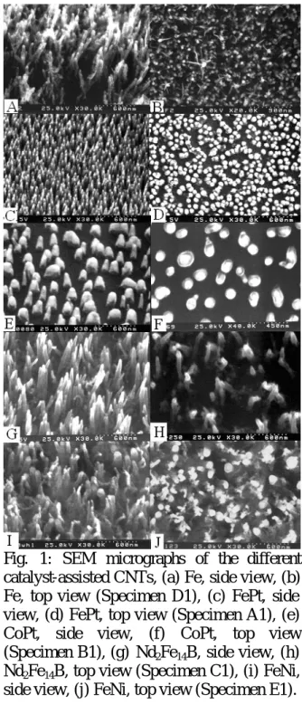
metal-assisted CNTs are shown in Table 2. The corresponding side view and top view SEM micrographs for different magnetic catalysts are depicted in Figs. 1(a) and 1(b), 1(c) and 1(d),… , 1(i) and 1(j) for Fe, FePt,
CoPt, Nb2Fe14B and FeNi catalysts,
respectively. From the point of applications in recording media, all CNTs here take advantages of the vertically aligned CNTs and the tip-growth CNTs instead of base-growth CNTs. The results show that at the same deposition conditions, different catalysts can produce CNTs with different morphology features and properties, such as, differences in tube number density, tube length, carbon film formation, bonding between catalyst and CNTs, growth mechanism and type of CNTs. These differences in structures or properties may relate to the solubility difference of carbon in catalysts, interaction of catalyst with the substrate, etching rate difference between CNTs and carbon films by hydrogen
solubility of nonferrous metals, such as Pt. In the present conditions, the maximum tube number density can go up to 134 Gtubes/inch2 for Fe-assisted CNTs. The tube number density can be one of the main factors determining the media recording density. The longest tube length can reach 2100 nm for 15 min deposition time for Nd2Fe14B–assisted CNTs, which is roughly corresponding to the highest growth rate. The highest coercive force is ~ 750 Oe for the Fe-assisted CNTs. It is interesting to note that the bamboo-like CNTs can be formed without using nitrogen gas, though nitrogen was proposed to be the main parameters to form the bamboo-like CNTs [10, 11]. For certain applications, if the removal of catalysts from tips of CNTs is required, it can easily be achieved by selecting proper catalyst and combining with ultrasonic agitation in acetone bath, e.g. FePt and CoPt catalysts.
The SEM micrographs for the magnetic metal-assisted CNTs or nano-particles for the catalysts with and without hydrogen plasma pretreatments can compare Figs. 1(a) with 2(a), 1(c) with 2(b), 1(e) with 2(c) for Fe, FePt and CoPt catalysts, respectively. It is obvious that morphologies of the carbon nanostructures are changed from tube-like to particle-like shapes by neglecting the hydrogen plasma pretreatment step. From the point of applications in recording media, the particle-like shapes take the advantages of short and rigid.
The typical lattice images or HRTEM images of the FeNi- and Fe-assisted CNTs close to the catalyst particles are shown in Figs. 3 and 4, respectively. In addition to the advantage of the vertically aligned CNTs, the catalysts at the tips of the CNTs are pear-like in shape, which favor greater contribution from magnetic shape anisotropy. The present process under ECR conditions with 875 Gauss magnetic field strength may also take the advantage of magnetic annealing effect to enhance the induced anisotropy. The magnetic properties and structure features of the magnetic catalyst-assisted CNTs are shown in Table 3.
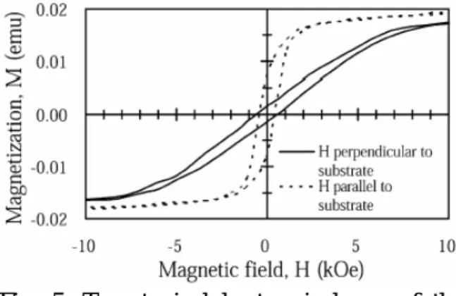
are shown in Fig. 5. The coercive forces of the Nd2Fe14B–assisted CNTs as a function of deposition temperature are shown in Fig. 6. It is obvious that the higher deposition temperature favors a greater coercive force and greater anisotropy. An abnormal greatest anisotropy at temperature greater than 700oC is not understood. It may relate to high enough temperatures to enhance magnetic annealing effect.
The AFM and the corresponding MFM images and MFM line scan profiles of the Fe-, FePt- and CoPt-assisted nano-particles or CNTs are revealed in Figs. 7(a) to 7(c), 7(d) to 7(f), and 7(g) to 7(i), respectively. The brighter and darker areas in MFM images represent the areas with repulsive and attractive magnetic forces with MFM probe, respectively. It implies that the magnetic particles are well distributed, and the magnetic fields of each particle can be detected or read.
4. Achievements and Self-commented
The five different magnetic materials were successfully used to act as catalyst to synthesize the magnetic metal-encapsulated CNTs or nano-particles on Si wafer to study the feasibility for perpendicular recording media applications. The results show that we can successfully deposit the perpendicularly- aligned magnetic particles-embedded nano- tubes and nano-particles. For recording media applications, the most of the deposited CNTs take the advantages of tip-growth CNTs and perpendicularly-aligned CNTs. The CNTs with different tube number density, tube length, carbon film formation, bonding between catalyst and CNTs, growth mechanism and type of CNTs can be manipulated by selecting different catalysts and pretreatments. These differences in structures or properties may relate to the solubility difference of carbon in catalysts, interaction of catalyst with the substrate, etching rate difference between CNTs and carbon films by hydrogen plasma. The tube number density is a key parameter determining the density of the recording media. In the present conditions, the maximum tube number density can go up to 134 Gtubes/inch2 for Fe-assisted CNTs.
Regard to the magnetic properties of the magnetic metal-encapsulated carbon nano- structures, the grain sizes of the magnetic particles (35 nm, or 10 ~ 100 nm in diameter) are greater than but close to the critical optimum size or single domain size, which favor a higher coercive force [11, 12]. A higher deposition temperature of CNTs results in a greater coercive force due to a smaller catalyst size, and the greatest coercive force can go up to 750 Oe for Fe-assisted CNTs at 715oC deposition temperature, which is comparable with the reported values in the literature [12-15]. The process also takes advantages of higher shape and induced anisotropy due to its higher aspect ratio and magnetic annealing effect. The coercive force difference between vertical and horizontal direction can reach 355 Oe in the present conditions. The results also demonstrate the potential applications in magnetic recording media that the isolated and well-distributed magnetic particles in the magnetic metal-encapsulated carbon nano- structures can be imaged by MFM micrographs.
References
[1] M. Todorovic, S. Schultz, J. Wong, and A. Scherer, Appl. Phys. Lett. 74 (1999) 2516. [2] D. E. Speliotis, J. Mag. and Mag. Mater. 193 (1999) 29.
[3] S. Y. Chou, Proc. IEEE 85 (1997) 652. [4] S. Y. Chou and P. R. Krauss, J. Mag. and Mag. Mater. 155 (1996) 151.
[5] S. Y. Chou, P. R. Krauss and L. Kong, J. Appl. Phys. 79(8) (1996) 6101.
[6] S. Iwasaki and K. Takemura, IEEE Trans. Mag. MAG-11 (5) (1975) 1173.
[7] S. Iwasaki and Y. Nakamura, IEEE Trans. Mag. MAG-13 (5) (1977) 1272. [8] R. L. White, J. Mag. and Mag. Mater. 209 (2000) 1.
[9] D. L. Leslie-Pelecky and R. D. Rieke, Chem. Mater. 8 (1996) 1770.
[10] X. Ma, E. Wang, D. A. Jefferson, J. Chen, S. Deng, N. Xu and J. Yuan, Appl. Phys. Lett. 75 (1999) 3105.
[11] H. L. Chang, C. H. Lin, C. T. Kuo, Diamond and Related Materials 11 (3-6) (2002) pp. 793-798.
R. Gao, Z. L. Wang, J. Mag. and Mag. Mater. 231(2001) L9.
[13] N. Grobert, W. K. Hsu, Y. Q. Zhu, J. P. Hare, H. W. Kroto, D. R. M. Waltona, M. Terrones, H. Terrones, Ph. Redlich, M. Ruehle, R. Escudero and F. Morales, Appl. Phys. Lett. 75 (1999) 3363.
[14] X. Sun, G. A. Yacaman, M. Jose, D. Xinglong, and J. Shouri, Mater. Sci. Eng. A 286 (2000) 157.
[15] T. Hayashi, S. Hirono, M. Tomita and S. Umemura, Nature 381 (1996) 772.
Fig. 1: SEM micrographs of the different catalyst-assisted CNTs, (a) Fe, side view, (b) Fe, top view (Specimen D1), (c) FePt, side view, (d) FePt, top view (Specimen A1), (e) CoPt, side view, (f) CoPt, top view (Specimen B1), (g) Nd2Fe14B, side view, (h) Nd2Fe14B, top view (Specimen C1), (i) FeNi, side view, (j) FeNi, top view (Specimen E1).
Fig. 2: SEM micrographs of the different catalyst-encapsulated carbon nano-particles neglecting catalyst H plasma pretreatment, (a) Fe (Specimen D2), (b) FePt (Specimen A2) and (c) CoPt (Specimen B2).
Fig. 3: Lattice image of the FeNi-assisted CNTs close to catalyst particle area (Specimen E1).
Fig. 4: HRTEM image of the Fe-assisted CNTs close to catalyst particle area (Specimen D1).
Fig. 5: Two typical hysteresis loops of the Nd2Fe14B-assisted CNTs at both vertical and horizontal directions to the substrate surface (Specimen C6).
Fig. 6: Coercive forces at vertical and horizontal directions versus deposition temperature for the Nd2Fe14B-assisted CNTs (Specimen C1 to C6).
Fig. 7: AFM image, MFM Image and the corresponding MFM line scan profile for different catalyst-assisted CNTs or nano-particles, respectively, (a), (b) and (c)
for Fe (Specimen D2); (d), (e) and (f) for FePt (Specimen A1); (g), (h) and (i) for CoPt (Specimen B2).
9
子計畫二:
電子迴旋共振化學汽相沉積反應腔體中電漿製程模擬
Plasma flow simulation for nanostructure formation in ECR-CVD
chamber
計畫編號:NSC 92-2120-M-009-001
執行期限:2003 年 8 月 1 日至 2004 年 7 月 31 日
主持人:吳宗信 國立交通大學 機械工程學系
中文摘要 在本研究計劃,吾人將以數值方法, 模擬用來製造奈米碳管等相關製程的電子 迴旋共振化學氣相沈積電漿源腔體,內部 中甲 烷/氫氣混合氣體電漿流場。在第一 年,硬體方面,吾人已成功建立及測試 23 節點、linux 作業系統的電腦叢集,以提供 電漿數值模擬使用。程式碼方面,電漿流 場模擬中,許多重要部分的程式碼也已陸 續完成測試,如下列所示:1.模擬靜電場分 佈所用的平行有限元素法 Poisson 方程式 程式碼 2.模擬靜磁場分佈所用的平行有限 元素法向量 Poisson 方程式程式碼 3.平行帶 電粒子運動及電磁場與電荷權重(PIC)程式 碼 。在未來第二年,吾人將對現正進行的 平行帶電粒子與中性原子間蒙地卡羅碰撞 法,和馬克思威爾方程程式碼,做進一步 的報告與說明。 關鍵詞:奈米碳管、迴旋共振化學氣相沈 積、Poisson 方程式、向量 Poisson 方程式、 馬克思威爾方程程式、PIC AbstractIn this project, we intend to simulate the plasma flow using methane/hydrogen gases as the precursors in an ECR-CVD (electron cyclotron resonance) chamber, which is used to manufacture nanotube-like structure in other related projects. In the first year, we have successfully built and tested a 23-node PC-cluster system in our laboratory, which runs Linux OS. This PC-cluster system shall be used for simulating plasma flow in the project as time continues. Several important components of the proposed simulation code have also been developed and verified. These include a parallel Poisson equation solver
using finite-element method (FEM) for simulating electrostatic distribution, a parallel Poisson vector potential solver using FEM for simulating magnetostatic distribution, a particle tracing module for moving charged particles under the influence of Lorentz force and a particle-in-cell (PIC) method for interpolating the force field (E and B) and charge between particles and grid points. Development of the Monte Carlo collisions (MCC), considering the collisions of charged particles and neutrals, and the Maxwell equation solver using FEM is currently in progress and shall be reported in the second year.
Keywords: plasma flow, finite element,
Poisson equation, Maxwell equation, particle in cell, Monte Carlo collision.
1. INTRODUCTION
In the other related project [1], ECR-CVD chamber has been used to manufacture nanostructures that can be potentially applied in higher-area-density magnetic recording media. The success of the materials processing forming nanostructures in this direction more or less depends upon trials-and-errors method. No systematic theoretical or modeling study has been
conducted. To optimize the materials
processing in forming nanostructures, fundamental understanding of the plasma flow inside the ECR-CVD chamber is inveitable, although it is very complicated in essence.
Materials processing plasmas have been modeled numerically using either the fluid model [2] or the particle model [3]. The fluid model is computationally much more efficient if mobility and diffusion coefficients are
provided in advance. The fluid model is valid when the electron density distribution is close to the Maxwellian. If the deviation cannot be neglected, the particle method has to be used for simulating the plasma. The particle method is a solution method for solving the Boltzmann equation. The particle method is a realization of this stochastic process using uniform random numbers (Monte Carlo simulation).
Advantages of the particle method include the justified application to low-pressure plasma as in the ECR-CVD chamber, energy distribution functions of electrons and ions as part of the solution, and unnecessary evaluation of mobilities, diffusion coefficients, and relaxation times for various values of reduced electric field, driving frequency and magnetic field.
The study was planned to be able to model the full-scale methane/hydrogen plasma flow inside the ECR-CVD chamber at the end of the three-year project. In this report, we describe briefly the preliminary results developed in this direction. In the following, numerical method
2. NUMERICAL METHOD
In this section, we will describe respectively the numerical methods employed for solving related governing equations.
2.1 Poisson Equation Solver
Poisson equation describing the
electrostatic distribution can be written as
0 2 ε ρ φ =− ∇ (1).
where φ (Ev =−∇φ) is the electric potential, is ε0 the permittivity and ρ is the net volumetric charge. In this research, we have applied Galerkin residual finite-element method to discretize equation (1). Resulting discretized equation can be written as follows,
(2), where Ni(e)is the shape function in node i.
equation from equation (2) is then solved using preconditioned conjugate gradient method (PCG).
2.2 Vector Potential Poisson Equation Solver
Vector Poisson Poisson equation describing the magnetostatic distribution can be written as follows,
J Ar 0r 2 =−µ
∇ (3)
in which the gauge condition has been enforced, Br=∇×Ar and Jr =∇×Mr . similarly, we have applied Galerkin residual finite-element method to discretize equation (3). Resulting discretized equation can be written as follows,
(4). Similarly, 3D tetrahedral mesh is used throughout the study unless otherwise specified. Resulting algebraic equation from equation (4) is then solved using preconditioned conjugate gradient method (PCG).
2.3 PIC/MCC method
The PIC method [4] was originally designed for collisionless charged particle simulations. It models the movement of charged particles under the influence of Lorentz force (F =q(E+v×B), q: particle charge, E: electric field, B: magnetic field) and solves the field equations (Maxwell or Poisson equation) due to redistribution of charge density (ρ) and charge current (J) at each time step. A mesh is introduced to sample the space charge and current distributions that enter the field equation. The sampling is performed by appropriate charge
assignment from the particle locations to the
grid points. Afterwards, the computed fields (E & B) from field equations at grid points are
interpolated back to the charge-particle
positions. Then, charged particles are moved to their new positions using the concept of
Boris rotation [3] without actually computing
the forces explicitly. This process repeats
O d t N µ dxdydz N M O d n M N a dxdydz z N z N y N y N x N x N µ O n e i x e i O x e i i j i e j e i e j e i e j e i x ∫∫ ∫∫∫ ∫∫ ∑∑ ∫∫∫ + ∇ × − × = ∂ ∂ ∂ ∂ + ∂ ∂ ∂ ∂ + ∂ ∂ ∂ ∂ − = = ) ( 0 ) ( ) ( 4 1 4 1 ) ( ) ( ) ( ) ( ) ( ) ( 1 ) ( ) ( ] ) ( [ 1 r r r O d t N dxdydz N e ? a dxdydz z N z N y N y N x N x N O n e i e i i j i e j e i e j e i e j e i x ∫∫ ∫∫∫ ∑∑ ∫∫∫ + = ∂ ∂ ∂ ∂ + ∂ ∂ ∂ ∂ + ∂ ∂ ∂ ∂ = = ) ( ) ( 4 1 4 1 ) ( ) ( ) ( ) ( ) ( ) ( ) ( ] ) ( [
In order to reproduce plasmas, one has to inevitably resolve the smallest time scale, i.e., electron time scale. It is estimated that electrons are the fastest particle in the plasma, with their velocities in the range of 105-106 m/s. Thus, this requires an electron time step of 10-10-10-9 s to properly model the electron trajectories in the presence of magnetic field. Thus, the time steps of ion and electron would be very much different to obtain the correct physics.
In addition, the so-called PIC/MCC method is to include the MC collisions, in the PIC method, between charged particles, and neutral particles and charged particles under the circumstances of weakly ionized plasma. This concept can be clearly shown in Fig. 1. The collisions between charged particles (or Coulomb collisions) are often neglected if low plasma density is concerned, as is the case in the bulk plasma region in DC-magnetron sputtering chamber. Only the collisions between charged particle and neutral particle will be taken into account in the current proposed study. In dealing with these collisions using Monte Carlo method, reliable cross section data are required.
2.4 Parallel Processing
Due to the expected high computational cost for PIC/MCC method and the necessity of solving the electrostatic/Maxwell equation at each electron/ion time step, parallel processing is strongly required for the practical purpose. We will present the proposed parallel processing, considering PIC/MCC method and field equation solver, in the following in turn.
2.4.1 Parallel PIC/MCC method
Since the MCC method is fundamentally a particle method that possesses high parallelism as the DSMC method, we will apply the similar parallel implementation using dynamic domain decomposition we have developed in our group [5]. Details can be found in this reference and references cited therein. We will only briefly describe the method here. In this parallel technique, Stop at rise (SAR) scheme is used, based on a degradation function, to detect the necessity of repartitioning of the computational domain
that uses multilevel graph-partitioning technique. In addition, the PIC method is only a way of interpolation of between nearby charged particles and nodal points; thus, it should pose no problem in parallelizing it.
2.4.2 Parallel field equation solvers
For parallel processing field equation (Poisson equation/vector potential Poisson equation/Maxwell equation), we need to formulate the system of equations in parallel format by storing the coefficient matrix in a distributed manner. As a first step, we will use the same grid distribution used by the PIC/MCC method since we expect the computational overhead in PIC/MCC would be much higher than that of solving field equation. We will solve equations using parallel version of preconditioned conjugate gradient method [6] using compressed-sparse-row (CSR) concept. In this method, we need to update the data at the interface nodes between sub-domains by communication using MPI.
3. RESULTS AND DISCUSSIONS 3.1 PC-Cluster System
We have built a 23-node PC-cluster system in our laboratory that were assembled and tested by ourselves. Main specifications inlcude 2.4GHz processor
ecah (AMD), 0.5GB RAM each and 1Gbps
Ethernet switch. We have been using Linux for all OSs since it is free and robust. System is now being used intensively for parallel processing. Pictures of these two systems are shown in Fig. 2
(http://www.me.nctu.edu.tw/~MuST).
3.2 Parallel Poisson Equation Solver
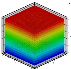
Completed parallel Poisson equation solver is verified by comparing the simulated data with analytical solution for a simplified one-dimensional parallel plate case. Test conditions include: 1000V at top plate, grounded at lower plate. Multilevel graph partitioning technique is used to partition the computational domain. Typical surface domain decomposition is illustrated in Fig. 3 for 20 processors using the number of nodes as the weighting criterion. Simulated
electrostatic potential distribution is shown in Fig. 4, which agrees with the analytical solution very well. Code has also been verified for other benchmark test cases, including concentric cylindrical shells (inner: high voltage, outer: grounded) and charged sphere under constant electric field. Results are compared excellently with analytical solutions. Study of parallel performance is currently in progress and will be reported in the future.
3.3 Parallel Vector Potential Poisson Equation Solver
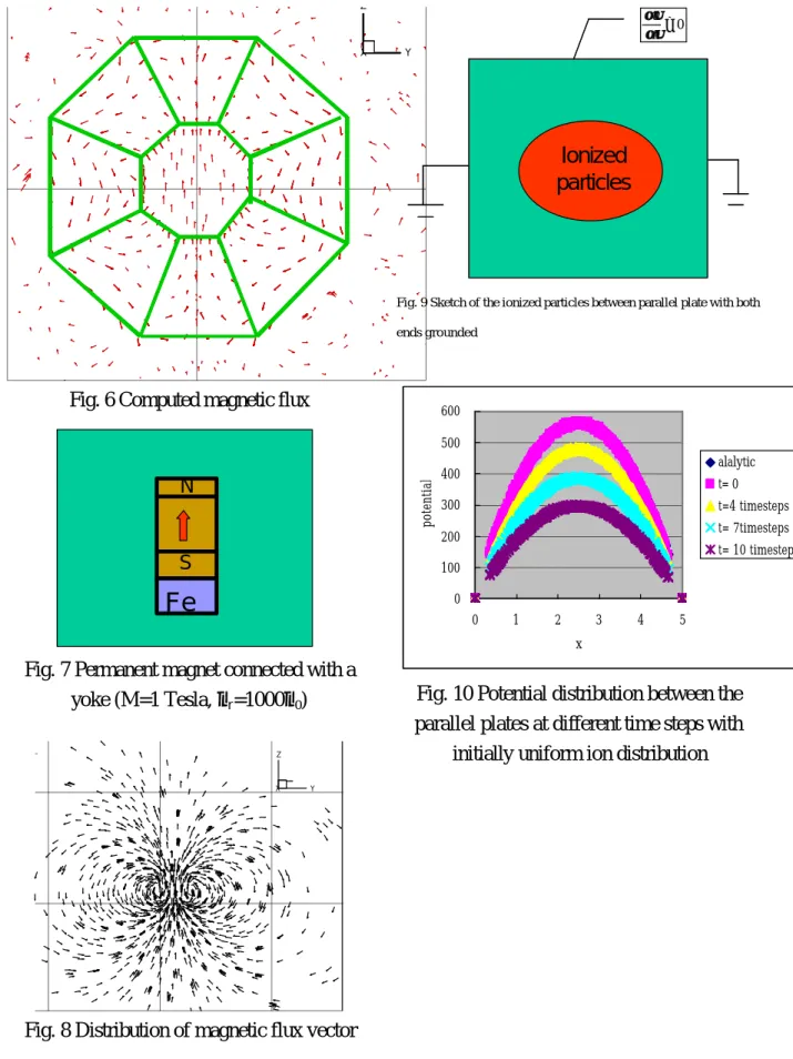
Permanent magnets arranged in octupus-shape (Fig. 5) are used to verify the completed parallel vector potential Poisson equation solver. 22 processors are also used for this simulation. Results of simulated magnetic flux vector are shown in Fig. 6 with 0.82 Tesla (upward) in the central airgap and are compared very well with the simulated data using commercial code such as Ansoft, which is often used in the magnetic society. Capability of simulating magnetostatic field having highly varying permeability is demonstrated using the test case of a permanent magnet (magnetization=1M Tesla upward), attached to a yoke (µr=1000µ0), as sketched in Fig. 7. Simulated magnetic flux vector is illustrated in Fig. 8, which clearly shows the excellent capability of this solver.
3.3 Coupled PIC and Poisson Equation solver
Completed parallel PIC method coupled with previous described Poisson equation solver is verified by computing a simplified 1-D parallel plate with both plates grounded and uniform ion distribution between the plates (Fig. 9). Ions collide with plates are absorbed (removed). 20 processors are used throughout the simulation. 10 particles per cell initially are used. Results of computed potential distribution are illustrated in Fig. 10 at various time steps. Results at t=0 compares very well with the exact solution.
4. CONCLUSIONS
with a parallel Poisson equation solver for electrostatic potential. Several works planned in the very near future are briefly summarized as follows:
1. To include the MCC collision into the parallel PIC-Poisson equation solver, which is currently in progress.
2. To develop a parallel Maxwell
equation solver based on the
previous experience in parallel Poisson equation solver.
3. To include the Maxwell equation
solver into the parallel PIC/MCC module.
4. To apply the above completed code to compute the methane/hydrogen plasma approximately beginning at the end of second year of the project.
References
1. 郭 正 次 : Fabrication and
characterizations of the alloy- encapsulated carbon nanostructures for applications in nano-resolution storage media and others. NSC 92-2120- M-009-001.
2. T. Makabe, Research Report 2000-2001, Lab. Plasma Electronics, Keio
University.
3. K. Nanbu, IEEE Plasma Science, Vol. 28 (2000), pp. 971-990.
4. Birdsall, C.K. and Langdon, A.B.,
Plasma Physics via Computer Simulation, McGraw-Hill, New York, NY, USA, 1985.
5. Wu, J.-S. and Tseng, K.-C., “Parallel DSMC method using dynamic domain decomposition,” 23rd Internal
Symposium on Rarefied Gas Dynamics, British Columbia, Canada, July, 2002. Also, AIP Conference Proceedings, Editors: Ketsdever, A.D. and Muntz, E.P., Vol. 663, pp.406-413, 2003. 6. Saad, Yousef, Iterative Methods for
Sparse Linear Systems, PWS Publishing Company, International Edition, 1996.
Fig. 1 Typical computational procedures
during a single time step for a PIC/MCC simulation
Fig. 2 23-node PC-Cluster system at MuST
Fig. 3 Surface domain decomposition for parallel Poisson solver (20 processors)
0 2 4 6 8 10 z 0 2 4 6 8 10 X 0 2 4 6 8 10 Y X
Fig. 4 Electrostatic potential distribution (colors are graded evenly in volts) (top
plate:1000 V, lower plate: 0 V)
Fig. 5 Permanent magnets arranged in an octopus-shape
X Y Z
Fig. 6 Computed magnetic flux
Fig. 7 Permanent magnet connected with a yoke (M=1 Tesla, µr=1000µ0)
X Y
Z
Fig. 8 Distribution of magnetic flux vector
Ionized
particles
0 = ∂ ∂ n uIonized
particles
0 = ∂ ∂ n uFig. 9 Sketch of the ionized particles between parallel plate with both
ends grounded 0 100 200 300 400 500 600 0 1 2 3 4 5 x potential alalytic t= 0 t=4 timesteps t= 7timesteps t= 10 timesteps
Fig. 10 Potential distribution between the parallel plates at different time steps with
initially uniform ion distribution N
S
子計畫三:
奈米結構沉積製程與積體電路製程之整合(1/3)
計畫編號:NSC 92-2120-M-009-001
執行期限:2003 年 8 月 1 日至 2004 年 7 月 31 日
主持人:潘扶民 國立交通大學 材料科學與工程學系
中文摘要 我們本計畫的第一年度內的主要研究內 容計有如下三項:(一) 製作陽極氧化鋁 (anodic aluminum oxide, AAO)自組裝奈米孔 洞陣列結構於六吋矽晶圓片上;(二) 以 AAO 奈米孔洞陣列結構做為版模,在矽基材或晶 圓上製作奈米點;(三) 開發奈米碳管(carbon nanotube, CNT) 選區成長與低溫成長製程技 術。我們成功地在六吋矽晶圓片製作出 AAO 版模,顯示了以 IC 製程技術將 AAO 圖案製 作在大尺寸矽晶片的可行性,我們亦成功地生長出與 AAO 相同陣列圖形的 TiO2及 SiGe
的奈米點陣列,並且發現限制奈米點尺寸可
提升 TiO2 介穩定晶相,anatase 相的穩定性;
在進行低溫成長 CNT 製程技術方面,以電漿 輔助化學氣相沉積法(plasma enhanced
chemical vapor deposition, PECVD),在 450oC 溫度下,在鈷金屬催化劑上成長出碳纖維, 顯示了低溫成長包覆合金的碳纖維的可行 性。
英文摘要
We have carried out three research tasks in the first project year: (1) fabrication of
self-assembly anodic aluminum oxide (AAO) nanopore array structure on 6 inch silicon wafers; (2) fabrication of nanodot arrays on silicon substrate using the AAO as the template; (3) develop a process technique to grow carbon nanotube (CNT) at low temperatures. We have successfully fabricated AAO nanopore arrays on the 6 inch silicon wafer, demonstrating the feasibility of integration of conventional integrated circuit process technology with the
fabrication process of AAO. We also
completed the growth of TiO2 and SiGe nanodot arrays on silicon substrates using the AAO as the template. The nanodot array structure is compliant with the nanopore array structure of the AAO template. We found deliberately control the size of the TiO2 nanodots can enhance the stability of the TiO2 anatase phase, which is a thermodynamically metastable phase. As to the low temperature growth of CNTs, in stead of the growth of CNTs, carbon nanofibers were found to be grown on the cobalt catalyst in a plasma enhanced chemical vapor deposition (PECVD) system at 450oC. From the result, it seems that the carbon nanofiber may act as a substituent for CNTs as an alloy-encapsulated carbon nanostructured materials.
關鍵詞
陽極氧化鋁,奈米碳管,電漿輔助化學氣相 沉積法,二氧化鈦,矽化鍺,奈米點, anodic aluminum oxide,AAO ,carbon nanotube,CNT,plasma enhanced chemical
vapor deposition,PECVD, TiO2, SiGe,
nanodot, (一) 前言 由於奈米科技領域所針對的研發對象多 是尺寸小於數十奈米的結構體,這些奈米結 構往往具有許多有趣特殊的物理化學特性, 藉著製作出奈米尺度的結構,我們可以觀察 到巨觀世界裡無法顯現出來的材料特性,將 這些特性應用於光電、能源、生化、環保等 科技領域,對人類文明的提昇可產生很大的
貢獻。為了發揮奈米結構材料的應用潛力, 普遍有效應用奈米科技的研發成果,必須要 能夠以低成本、量產的方式製作奈米結構材 料,目前能夠以經濟規模製作奈米尺度產品 的技術只有半導體的積體電路技術,不過受 限於微影製程的技術瓶頸,90 奈米是目前 IC 產業可以達到經濟規模製作之最小結構尺 寸,更小的結構仍有待開發,如果利用先進 的奈米結構材料製作技術,是可以克服現有 IC 微影製程技術的極限,不過目前許多具應 用潛力的奈米材料與現代矽基積體電路技術 有材料製程相容性的問題,如何整合奈米結 構材料製程與 IC 製程技術是本計畫的研究 課題。 在所有奈米結構材料裡,奈米碳管 (carbon nanotube, CNT)是被研究最廣泛的奈 米材料,其電性可是半導體,亦可屬於金屬 類(1-3),所以可被運用於場效電晶體中的閘 極通道,或做為低電阻、高抗電遷移 (electromigration)的穩定導線,並被做為場發 射三極體中的電子發射源,CNT 具有優良的 機械強度,並因有奈米尺度的管徑,毫米長 度的管體,所以有許多研究團隊開發出以 CNT 為針頭的原子力顯微鏡探針(4-6)。此 外,利用化學氣相沉積的 CNT 必須以鐵鈷? 等鐵磁性金屬做為生長 CNT 的催化劑,如果 藉此生長機制設計出適當的 CNT 製程條 件,將鐵磁性合金材料包覆於 CNT 內,則可 能製作出高解析高密度的記憶儲存媒體。前 述 CNT 的各種應用,多數須要先將催化劑金 屬奈米顆粒沉積於諸如矽晶的基材上,再成 長 CNT 於金屬粒上,許多 IC 製程整合的問 題便延伸出來,例如選區定點沉積催化劑金 屬奈米粒是否與現代 IC 製程技術相容,能否 在大面積基材上沉積與成長均勻的奈米點結 構或是碳奈米管。 方法製備奈米結構材料的技術被發展出來, 這些技術多具有一個共同的缺點,乃是無法 得到控制均勻的結構與形貌分佈,這種缺點 會使得整合這些奈米結構材料於元件或功能 性模組時,形成製程的瓶頸。本計畫研究重 點目標即是探討並解決這些整合的問題。如 上段所述,90 奈米線寬結構是現代量產 IC 微影製程技術的一個最小極限,為了製作更 小尺寸的結構,必須採用非傳統光學的微影 技術,例如電子束或掃描探針微影術(7-8), 但是這些技術的製作速度尚未能達到量產的 要求,奈米結構材料若是藉由這類微影技術 一一製作,耗費的時間與成本將相當驚人, 如果由奈米結構以自發性與規則性地大量成 長出來,便可以減少或甚至避免使用成本昂 貴的微影製程,這種自發、規則性成長奈米 結構材料可藉由自組裝成長方式達成;在此 一研究計畫裡,我們擬利用依自組裝原理製 作而成的奈米孔洞材料,如陽極氧化鋁 (anodic aluminum oxide, AAO)作為版模製作 奈米結構材料,如奈米晶、量子點及奈米管 等,並以 IC 製程技術定義奈米陣列結構圖 案,依研究者的設計需求,整合不同尺度的 製程技術於矽晶片上,可以有效集結放大奈 米結構材料特殊的磁光電特性。 (二) 研究目的: 基於前述前言背景的說明,本計劃的研 究目的為研發出奈米結構材料與現代 IC 技 術製程整合的方法,基本上,研究目標有二 個方向:(一) 發展相容於現代矽基 IC 製程技 術之奈米結構材料製程及 CNT 低溫成長製 程, (二) 展示 AAO 版模技術作為奈米材料 結構的製作平台的可行性。 (三) 研究方法 在第一年的計畫工作裡,我們進行了以 下的工作內容:(一) 製作 AAO 版模於六吋
17 成長製程技術。 為了整合奈米結構材料與現代 IC 技術製程,奈米材料必須成長於矽晶圓片 上,才能夠有效配合現代 IC 製程設備,進行 奈米結構的大量製造,在此研究中,我們以 六吋正型矽晶圓做為基材,不過在許多非關 鍵的製程研究裡,我們亦使用不完整的矽晶 破片,以節省材料成本。在 AAO 版模的研製 上,有別於大多 AAO 研究團隊使用鋁箔製作 AAO,我們直接將 AAO 製作在矽基材上,我 們將數微米的鋁金屬膜以物理氣相沉積方法 鍍在矽基材上,鋁金屬靶材均為 99.999 的純 鋁,在四吋或矽晶破片上,以蒸鍍法沉積鋁 膜,離子濺鍍法則用於六吋晶圓。 我們以草 酸做為電解液製作 AAO,將矽晶破片置入實 驗燒杯內,在室溫下進行電解;至於六吋晶 圓上 AAO 的製作,我們利用一般大試片電鍍 槽,經過簡易的改裝,作為六吋晶圓的電解 槽,由於鋁膜表面粗糙度會嚴重影響 AAO 的 品質,我們在濺蝕沉積鋁膜後,會進行退火 及化學機械研磨(chemical-mechanical polishing)處理。本實驗電解液是 0.3M 的草 酸,溫度在 10~25℃ 工作電壓為 40V,本實 驗也嘗試用 10wt﹪磷酸溫度約 10℃工作電 壓為 100~160V,得到大範圍規則排列的鋁陽 極氧化膜是本實驗的首要目的。 在矽晶圓上製作奈米點方面,我們在第 一階段,利用 AAO 版模在矽基材上製作二氧
化鈦(TiO2)與矽化鍺(SiGe)奈米點, TiO2奈
米點的製作是將氮化鈦(TiN)薄膜鍍在矽晶 片後,再沉積 Al 膜於其上,當電解 Al 膜所 形成 AAO 孔洞陣列底部逐漸接近 TiN 薄膜 界面時,TiN 會因電解液的擴散而被氧化, 其氧化區域受到 AAO 孔洞陣列圖形的制 約,於是當將上層之 AAO 層移除後,具有與 AAO 孔洞陣列圖案相似的 TiO2奈米點陣列 便形成於矽晶片上(9),圖一為該奈米點陣列 製作之流程圖;至於 SiGe 奈米點的製作,則 是一種 TiO2奈米點陣列結構製作的延伸,我 們利用超高真空化學氣相沉積法(UHV-CVD) 先在矽晶片上沉積一層 SiGe 薄膜,隨後如前 述 TiO2奈米點製作步驟,依序鍍上 TiN 與 Al 膜,電解過後所形成的 TiO2奈米點結構被 用來做為乾蝕刻 SiGe 層的硬質遮罩,經過傳 統的 IC 製作程序後,便可在矽晶圓上製作出 與 AAO 孔洞陣列相同的 SiGe 奈米點陣列圖 案,SiGe 奈米點陣列之製作流程顯示於圖 二;至於鐵、鈷、鎳奈米點陣列的圖案可以 利用相似的製作方法,或直接在已形成之 AAO 孔洞陣列上進行 CVD 或無電鍍法製作。 為了在特定區域內成長奈米結構材料, 必須發展出適當的奈米材料選區成長技術, 以成長 CNT 為例,金屬催化劑(鐵、鈷、鎳) 奈米點的位置決定了 CNT 的生長的位置,我 們將 AAO 版膜整合於現代的積體電路製程 技術,用來成長高準直性的高密度陣列奈米 碳管; 具預先定義表面圖案之 AAO 膜先被 製作在的矽晶圓上,鈷或鎳因與 IC 製程技術 相容性高,被做為 CNT 的催化劑,當以 PVD 鍍膜方式製作催化劑奈米點,我們會運用前 述製作 TiO2奈米結構的類似製程技術,但是 奈米點的最終位置會與 AAO 孔洞陣列位置 呈現互補關係,CNT 隨後成長於其上;無電 鍍沉積鈷或鎳於 AAO 孔洞內亦是我們選擇 製作催化劑奈米點的另一製程方法,這一方 法直接將鈷或鎳沉積入 AAO 孔洞內,CNT 可以成長於 AAO 內,或在移除 AAO 後,成 長於鈷、鎳奈米點上;由於現在的 IC 製程技 術在後段連線製程上,製程溫度均小於 450oC,而現有之 CNT 成長溫度多高於 600oC,如何降低 CNT 成長溫度是成功整合 CNT 於 IC 製程技術的關鍵,我們嘗試改善催 化劑奈米點的前處裡條件及以電漿輔助 CVD(PECVD)系統來成長低溫 CNT。 (四) 結果與討論
我們就第一年度之數項研究內容分別進 行討論其研究結果:
(一) 利用 AAO 版模在矽基材上製作奈米點 在此計畫年度之前,我們已完成了製作
TiO2奈米點於矽晶片上(9),TiO2奈米點是由
AAO 版膜下的 TiN 薄膜直接在 AAO 的電解 液下直接氧化而成;這一年度起,我們持續 改善 TiO2奈米點陣列之品質,圖三為 AAO 孔洞陣列與 TiO2奈米點陣列之 SEM 表面影 像,從圖三中可知 TiO2奈米點陣列之排列圖 案與 AAO 孔洞陣列圖案有對應的關係,研究 過程中,我們發現蒸鍍鋁金屬膜較之濺鍍鋁 膜可以得到較具規則性的 AAO 孔洞陣列,這 可能是因為濺鍍與蒸鍍兩種沉積方式所造成 的鋁金屬膜晶粒大小及缺陷密度不同所致, 濺鍍法有較粗糙的表面與較多的缺陷,以電 解拋光處理可以得到頗為平整的表面,400o C 退火被用來消減 PVD 鋁膜的缺陷與促進晶 粒成長,但是因為高溫爐管系統污染原因, 改善 PVD 鋁膜的退火處理條件依然在進行 中;我們針對所製作出來之 TiO2奈米點進行 微結構相的變化,TiO2有三種結晶相,rutile,
anatase 與 brookite,熱力學穩定相為 rutile
相,在 TiO2晶粒成核至約 15 nm 左右會以 anatase 介穩定相存在,但隨晶粒成長逐漸轉 變為 rutile 相,但在我們所形成的 TiO2奈米 點陣列中,即使加熱至 1000o C,anatase 相依 然穩定存在,這是由於奈米點陣列所擁有的 大表面積,太大的表面能使得 rutile 相無法順 利成長,由此研究結果證實我們可以藉著控 制奈米點尺寸,製作出優選 anatase 相的奈米 點陣列的薄膜,如此便可利用各相特殊的材 料特性,這一研究結果已發表於 Appl. Phys. Lett. (10)。 此外,我們利用 TiO2奈米點陣列做為蝕 刻 SiGe 薄膜的硬質遮罩以製作相同圖案之 奈米點陣列,圖四為做為乾蝕刻硬質遮罩之 與 SiGe 乾蝕刻後, SEM 的影像(圖四)顯示 SiGe 奈米點的大小在 60 nm 上下。 雖然 SiGe 的奈米點外形輪廓不若硬遮罩 TiO2奈米點平整,但是陣列規則性是對應一 致的,我們正尋找奈米點表面平整化的處裡 條件。 (二) 製作 AAO 版模於六吋晶圓片; 我們在進行六吋矽晶圓 AAO 製作時,先經濕 式清洗晶圓,用 CVD 方式在晶圓上沉積一層 約 20nm 的 TiN 當作擴散阻絕層,完成後再 濺鍍一層金屬鋁,膜厚約 4µm。經 400℃真 空退火處理,消除在濺鍍時所產生的內應 力,再以化學機械研磨表面。圖五為在 0.3M 草酸、電壓 40V 在溫度 10℃經過鋁陽極氧化 處理後 AAO 的 SEM 影像。如圖所示,孔徑 的大小差別不是很大,孔洞間距平均都在 0.1µm 左右,室溫 25℃製作的 AAO 的洞距與 排列並沒有明顯差異,由於氧化的初期如果 表面粗糙或者有缺陷,都會造成局部電場的 強度變化,進而影響自組裝 AAO 內部孔洞通 道的應力紓解機制,會導致 AAO 洞距與陣列 的不規則排列與分佈,從圖圖五觀查,我們 初步已可在六吋矽晶圓上製作具自組裝排列 特性的 AAO 孔洞陣列結構,在六吋晶圓內各 區的均勻性亦非常好;比較小試片上製作的 AAO 孔洞陣列,雖然圖五的 AAO 結構依然 較不規則,但此項研究結果顯示利用一般 IC 的製程步驟將 AAO 圖案製作在大尺寸矽晶 片上是可行的。 不管在小試片或六吋矽晶圓上製作 AAO,基本上,整齊規則的 AAO 陣列結構區 域是有侷限的,從前列的 SEM 影像中,我們 可清楚觀查到具規則排列週期的 AAO 陣列 區域大小多在~1 µm 以下,依照文獻報導, 欲形成大範圍的孔洞陣列,可在進行 AAO 電 解前,先在鋁金屬表面預做洞距為 0.1 - 0.2 µm 的 AAO 孔洞陣列圖形,再導引 AAO 的 孔洞成長方向(11),目前我們嘗試利用電子束 (e-beam)微影製程,作出孔徑大小 0.1- 5μm 的光阻圖案。由於微影製程設施的限制,我 們無法曝出小於 0.2μm 的孔徑,因此在經過
19 以上,在經 0.3M 草酸、電壓 40V、溫度 25℃、 時間 10 min 的 AAO 處裡,凹孔區內亦產生 了 AAO 的圖形,如圖六所示,顯示我們目前 的工具無法達到控制大面積 AAO 規則陣列 的成長。我們未來將嘗試利用所謂之奈米壓 印(nano imprint)技術來改善圖案製作的孔洞 間距解析度問題,這種壓印技術可大量製作 高密度奈米結構(12-13)。 (三) CNT 低溫成長製程。 現代 IC 製程技術的連線製程溫度均小於 450oC,如何降低 CNT 成長溫度是成功整合 CNT 於 IC 製程技術的關鍵,本實驗嘗試降低 奈米碳管的製備溫度;利用 r.f.-PECVD(13.56 MHz) 系統製備 CNT,觸媒為鈷,先經過氫 電漿處理後,再通入甲烷及氫氣成長 CNT, 圖七為所製備出之碳奈米材料之 SEM 影 像,該製備溫度為 400 o C,壓力 10 mTorr, 甲烷與氫氣流量分別為 20 s.c.c.m.與 80 s.c.c.m,成長時間 30 分鐘;如圖所示,觸媒 顆粒大小約為 100 nm,觸媒表面有許多的短 鬚,長度在 15 nm 左右,由 TEM 影像圖八觀 查,短鬚呈實心,直徑約在 50 nm 左右,似 乎是碳纖維(carbon fiber),部分碳纖維在頂部 可發現觸媒存在,他們的排列並不規則,依 據文獻報導(13),PECVD 在低溫(300o C 以下) 下可以生長出碳纖維,我們的研究似乎亦有 相似的結果,但我們的碳纖維較短小不規 則,可能是由於成長氣壓偏低,同時試片未 施加偏壓,目前正調整成長條件,包括試片 偏壓,溫度與氣體流量與壓力;由目前的結 果顯示低溫成長包覆合金的碳纖維是可行 的,原始的構想以成長 CNT 為目標,不過就 應用面而言,若奈米探管是為了用以支撐及 定位合金奈米顆粒,包覆合金的碳纖維與包 覆合金的 CNT 是不會有太大的差異的。 (五) 結語 在這計畫的第一年度內,我們進行了三 項的研究內容,(一) 在六吋矽晶圓片上製作 AAO 版模;(二) 利用 AAO 版模在矽基材或 晶圓上製作奈米點;(三) 開發 CNT 選區成 長與低溫成長製程技術。我們已成功地在六 吋矽晶圓片製作出 AAO 版模,雖然該 AAO 結構規則性須要加以改進,但此項研究結果 顯示利用 IC 的製程步驟將 AAO 圖案製作在 大尺寸矽晶片上是可行的,此外,我們以 AAO 做為版模,成功翻印生長相同排列圖形
的 TiO2及 SiGe 的奈米點陣列,我們由 TiO2
奈米點的晶相觀查,發現可藉限制奈米點尺 寸來控制 TiO2 anatase 相的穩定性,提升了 anatase 相的應用價值;在進行低溫成長 CNT 製程技術方面,初步結果並沒有成長出 CNT 出來,反而是在 450oC 溫度下,於鈷奈米粒 上成長出碳纖維,不過結果顯示了低溫成長 包覆合金的碳纖維的可行性,PECVD 設施與 製程條件的改進正同時進行中。 (六) 參考文獻
(1) M. Shiraishi, M. Ata, Syn. Metals 128 (2002) 235.
(2) A. Javey, M. Shim, and H. Dai, Appl. Phys. Lett., 80,(2002) 1064.
(3) T. W. Odom, J.-L. Huang, P. Kim, and C. M. Lieber, J. Phys. Chem. B, 104 (2000) 2794. (4) H. Dai, J. H. Hafner, A. G. Rinzler, D. T. Colbert, and R. E. Smalley, Nature, 384, 147 (1996).
(5)S. S. Wong, A. T. Woolley, T. W. Odom, J.-L. Huang, P. Kim, D. V. Vezenov, and C. M. Lieber, Appl. Phys. Lett. 73, 3465 (1998). (6) J. H. Hafner, C.-L. Cheung, T. H.
Oosterkamp and C. M. Lieber, J. Phys. Chem. B, 105, 744 (2001).
(7) B. Irmer, M. Kehrle, H. Lorenz and J. P. Kotthaus., Appl. Phys. Lett. 71, 1733 (1997). (8) F. S. S. Chien, J. W. Chang, S. W. Lin, Y. C. Chou, T. T. Chen, S. Gwo, T.-S. Chao and W.-F. Hsieh, Appl. Phys. Lett. 76, 360 (2000).
(9) P.L. Chen, C.T. Kuo, T.G. Tsai, B.W. Wu, C.C. Hsu and F.M. Pan, , J. Appl. Lett., 82 (2003) 2796-2798.
(10) P. L. Chen, C. T. Kuo, F. M. Pan and T. G. Tsai, Appl. Phys. Lett.,84 (2004) 3888.
(11) H. Tan, L. Kong, M. Li, C. Steer and L. Koecher, SPIE, (2004)
(12) S. Y. Chou, MRS Bulletin, July (2001) 512.
(13) S Hofmann, B Kleinsorge, C Ducati
and J Robertson, New J. Phys. 5 (2003) 153.
Si wafer PVD TiN鍍膜 蒸鍍或濺鍍Al膜 (厚 度> 4 µm) 於草酸水溶液中電解,分 兩階段電解,形成AAO奈 米孔洞陣列 以HgCl2移除AAO,產生 TiO2奈米點陣列於Si 基 材上 圖一:TiO2奈米點陣列製作之流程。 Si wafer PVD TiN鍍膜 蒸鍍或濺鍍Al膜 (厚度> 4 µm) 於草酸水溶液中電解,形成AAO 奈米孔洞陣列 以HgCl2移除AAO,產生TiO2奈米點 陣列於Si 基材上 UHV-CVD SiGe鍍 膜沉積 以TiO2奈米點為遮罩,蝕刻下層TiN 與SiGe 移除TiN ,產生SiGe奈米點 陣列 圖二:SiGe 奈米點陣列之製作流程。
21 500 nm 圖三:AAO 孔洞陣列(上)與 TiO2 奈米點陣列(下)之 SEM 影像。 圖四:乾蝕刻硬質遮罩之 TiO2(上) 奈 米點陣列及蝕刻後之 SiGe (下)奈米點 陣列的 SEM 影像。 圖五:在 0.3M 草酸,工作電壓 40V,10oC 經過鋁陽極氧化處理 後的 SEM 影像。 圖六:利用電子束微影製程在鋁金 屬表面預做 AAO 陣列圖形凹孔,再 進行 AAO 電解,凹孔區內亦產生了 AAO 的圖形、
圖七:PECVD 所製備出之碳奈米材料之 SEM 影像,製備溫度為 400 oC,觸媒顆粒 大小約為 100 nm,觸媒表面有許多的短 鬚,長度在 15 nm 左右。 圖八:碳纖維 TEM 影像,直 徑約在 50 nm 左右,觸媒存在 於部分碳纖維頂部。